


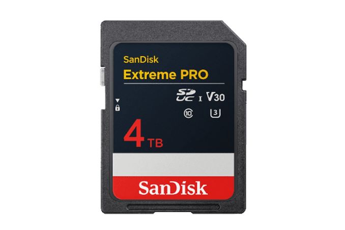
Western Digital this week is previewing the industry's first 4 TB SD card. The device is being showcased at the NAB trade show for broadcasters and content creators and will be released commercially in 2025.
Western Digital's SanDisk Extreme Pro SDUC 4 TB SD card complies with the Secure Digital Ultra Capacity standard (SDUC, which enables up to 128TB). The card uses the Ultra High Speed-I (UHS-I) interface and is rated for speed Class 10, therefore supporting a minimum speed of 10 MB/s and a maximum data transfer rate of 104 MB/s when working in UHS104 (SDR104) mode (there is a catch about performance, but more on that later). WD's SD card is also rated to meet Video Speed Class V30, supporting a minimal sequential write speed of 30 MB/s, which is believed to be good enough for 8K video recording, above and beyond the 4K video market that Western Digital is primarily aiming the forthcoming card at.
For now, Western Digital is not disclosing what NAND is in the SanDisk Extreme Pro SDUC 4 TB SD card. Given the high capacity and relatively distant 2025 release date, WD may be targetting this as one of their first products to use their forthcoming BiCS 9 NAND.
And while not listed in WD's official press release, we would be surprised if the forthcoming card didn't also support the off-spec DDR200/DDR208 mode, which allows for higher transfer rates than the UHS-I standard normally allows via double data rate signaling. Western Digital's current-generation SanDisk Extreme Pro SDXC 1 TB SD card already supports that mode, allowing it to reach read speeds as high as 170 MB/s, so it would be surprising to see the company drop it from newer products. That said, the catch with DDR208 remains the same as always: it's a proprietary mode that requires a compatible host to make use of.
Western Digital has not disclosed how much will its SanDisk Extreme Pro SDUC 4 TB SD card cost. A 1 TB SanDisk Extreme Pro card costs $140, so one can make guesses about the price of a 4 TB SD card that uses cutting-edge NAND.
Storage
While desktop PC power supplies receive the bulk of enthusiasts’ attention for good reasons – not the least of which being the vast selection of options that comes from being a standardized part – power supplies as a whole aren’t just a concern for big PCs. With the majority of PC sales having flipped to notebook sales some years ago, notebook power supplies already lead the market in volume. And while most laptops don’t need the kind of massively powered PSUs that dominate the desktop space, even that is slowly changing as desktop replacement-class laptops increasingly grow in performance and power consumption.
Perhaps the poster-child for the high-performance, high-powered laptop is Eurocom, who has a long history of developing heavy-duty DTR laptops that are all but portable desktop systems. Following recent trends in GPU power consumption and in GPU popularity for both gaming and AI workloads, the company has been selling a range of “mobile supercomputers”, which are practically large, tailor-made laptops that rival even the best of desktop computers – and have the power requirements to match.
In order to power their own high-end laptops, Eurocom has developed a rather unusual 780W AC adapter for high-performance laptops. Intended to power the most powerful of powerful laptops, their latest power adapter can supply over three-quarters of a kilowatt of DC power; a desktop-like wattage for a desktop-like device. It’s a laptop power adapter that’s unique in its scale, and with some room to scale up even further.
| Eurocom 780W AC Adapter Power specifications |
|
| RAIL | +20V |
| MAX OUTPUT | 39A |
| 780W | |
| DIMENSIONS | 325 x 110 x 40mm, 1.38kg |
| AC INPUT | 90 - 264 VAC, 50 - 60 Hz |
| MSRP | PSU: $299, Cable: $129+ |
Eurocom has offered this adapter for a few years now. But it’s taken on a new life as more laptops have been released that use such a large adapter (or two smaller 300W-ish power adapters). And, critically, Eurocom has made additional DC cable/connector sets for other manufactuers’ laptops, significantly increasing the number of systems it’s compatible with. Currently, Eurocom offers DC cables for the following laptops:
Externally, the Eurocom 780W AC adapter looks like a hybrid between a PC PSU and a laptop adapter. It is shaped like an oversized laptop AC adapter but has a metallic body and cooling vents/fans. Eurocom advertises that it weighs “only 1.34kg”, which is the weight of an entire 14-inch laptop by comparison, but is relatively lightweight for a PSU with that kind of power output. The company logo is debossed across the top side of the adapter, with four round anti-slip pads found at its bottom. Care needs to be taken while moving it around because the metallic edges and weight can spell trouble for wooden surfaces.
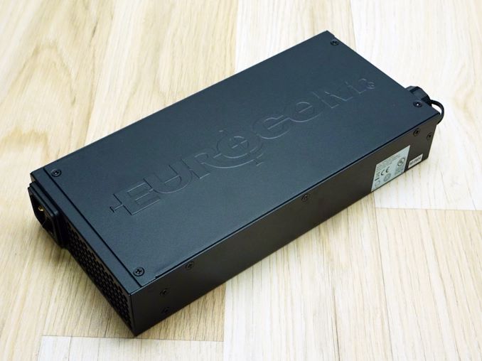
Eurocom installed a small information display on the AC adapter, which shows the current, voltage, and power output, as well as the temperature of the adapter. It is not perfectly accur... Cases/Cooling/PSUs

Across the internet, from online forums such as Reddit to various other tech media outlets, there's a lot of furor around reports of Intel's top-end 14th and 13th Gen K series of processors running into stability issues. As Intel's flagship chips, these parts come aggressively clocked in order to maximize performance through various implementations of boost and turbo, leaving them running close to their limits out of the box. But with high-end motherboards further goosing these chips to wring even more performance out of them, it would seem that the Intel desktop ecosystem has finally reached a tipping point where all of these efforts to boost performance have pushed these flagship chips to unstable conditions. To that end, Intel has released new gudiance to its consumer motherboard partners, strongly encouraging them to actually implment Intel's stock power settings, and to use those baseline settings as their out-of-the-box default.
While the underlying conditions are nothing new – we've published stories time and time again about motherboard features such as multi-core enhancement (MCE) and raised power consumption limits that seek to maximize how hard and how long systems are able to turbo boost – the issue has finally come to a head in the last couple of months thanks to accumulating reports of system instability with Intel's 13900K and 14900K processors. These instability problems are eventually solved by either tamping down on these motherboard performance-boosting features – bringing the chips back down to something closer to Intel's official operating parameters – or downclocking the chips entirely.
Intel first began publicly investigating the matter on the 27th of February, when Intel's Communications Manager, Thomas Hannaford, posted a thread on Intel's Community Product Support Forms titled "Regarding Reports of 13th/14th Gen Unlocked Desktop Users Experiencing Stability Issues". In this thread, Thomas Hannaford said, "Intel is aware of reports regarding Intel Core 13th and 14th Gen unlocked desktop processors experiencing issues with certain workloads. We're engaged with our partners and are conducting analysis of the reported issues. If you are experiencing these issues, please reach out to Intel Customer Support for further assistance in the interim."
Since that post went up, additional reports have been circulating about instability issues across various online forums and message boards. The underlying culprit has been theorized to be motherboards implementing an array of strategies to improve chip performance, including aggressive multi-core enhancement settings, "unlimited" PL2 turbo, and reduced load line calibration settings. At no point do any of these settings overclock a CPU and push it to a higher clockspeed than it's validated for, but these settings do everything possible to keep a chip at the highest clockspeed possible at all times – and in the process seem to have gone a step too far.
From "Why Intel Processors Draw More Power Than Expected: TDP and Turbo Explained"
We wrote a piece initially covering multi-core enhancement in 2012, detailing how motherboard manufacturers try to stay competitive with each other and leverage any headroom within the silicon to output the highest performance levels. And more recently, we've talked about how desktop systems with Intel chips are now regularly exceeding their rated TDPs – sometimes by extreme amounts – as motherboard vendors continue to push them to run as hard as possible for the best performance.
But things have changed since 2012. At the time, this wasn't so much of an issue, as overclocking was actually very favorable to increasing the performance of processors. But in 2024 with chips such as the Intel Core i9-14900K, we have CPUs shipping with a maximum turbo clock speed of 6.0 GHz and a peak power consumption of over 400 Watts, figures that were only a pipe dream a decade ago.
Jumping to the present time, over the weekend Intel released a statement about the matter to its partners, outlining their investigation so far and their sug... CPUs

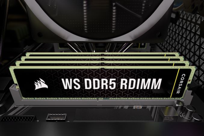
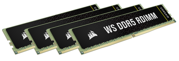
Corsair has introduced a family of registered memory modules with ECC that are designed for AMD's Ryzen Threadripper 7000 and Intel's Xeon W-2400/3400-series processors. The new Corsair WS DDR5 RDIMMs with AMD EXPO and Intel XMP 3.0 profiles will be available in kits of up to 256 GB capacity and at speeds of up to 6400 MT/s.
Corsair's family of WS DDR5 RDIMMs includes 16 GB modules operating at up to 6400 MT/s with CL32 latency as well as 32 GB modules functioning at 5600 MT/s with CL40 latency. At present, Corsair offers a quad-channel 64 GB kit (4×16GB, up to 6400 MT/s), a quad-channel 128GB kit (4×32GB, 5600 MT/s), an eight-channel 128 GB kit (8×16GB, 5600 MT/s), and an eight-channel 256 GB kit (8×32GB, 5600 MT/s) and it remains to be seen whether the company will expand the lineup.
Corsair's WS DDR5 RDIMMs are designed for AMD's TRX50 and WRX90 platforms as well as Intel's W790 platform and are therefore compatible with AMD's Ryzen Threadripper Pro 7000 and 7000WX-series as well as Intel's Xeon W-2400/3400-series CPUs. The modules feature both AMD EXPO and Intel XMP 3.0 profiles to easily set their beyond-JEDEC-spec settings and come with thin heat spreaders made of pyrolytic graphite sheet (PGS), which thermal conductivity than that of copper and aluminum of the same thickness. For now, Corsair does not disclose which RCD and memory chips its registered memory modules use.
Unlike many of its rivals among leading DIMM manufacturers, Corsair did not introduce its enthusiast-grade RDIMMs when AMD and Intel released their Ryzen Threadripper and Xeon W-series platforms for extreme workstations last year. It is hard to tell what the reason for that is, but perhaps the company wanted to gain experience working with modules featuring registered clock drivers (RCDs) as well as AMD's and Intel's platforms for extreme workstations.
The result of the delay looks to be quite rewarding: unlike modules from its competitors that either feature AMD EXPO or Intel XMP 3.0 profiles, Corsair's WS DDR5 RDIMMs come with both. While this may not be important on the DIY market where people know exactly what they are buying for their platform, this is a great feature for system integrators, which can use Corsair WS DDR5 RDIMMs both for their AMD Ryzen Threadripper and Intel Xeon W-series builds, something that greatly simplifies their inventory management.
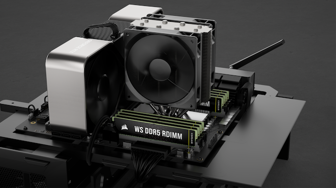
Since Corsair's WS DDR5 RDIMMs are aimed at workstations and are tested to offer reliable performance beyond JEDEC specifications, they are quite expensive. The cheapest 64 GB DDR5-5600 CL40 kit costs $450, the fastest 64 GB DDR5-6400 CL32 kit is priced at $460, whereas the highest end 256 GB DDR5-5600 CL40 kit is priced at $1,290.
Memory
AMD has recently expanded its Ryzen 8000 series by introducing the Ryzen 7 8700F and Ryzen 5 8400F processors. Initially launched in China, these chips were added to AMD's global website, signaling they are available worldwide, apparently from April 1st. Built from the recent Zen 4-based Phoenix APUs using the TSMC 4nm node as their Zen 4 mobile chips, these new CPUs lack integrated graphics. However, the Ryzen 7 8700F does include the integrated Ryzen AI NPU for added capabilities in a world currently dominated by AI and moving it directly into the PC.
The company's decision to announce these chips in China aligns with its strategy to offer Ryzen solutions at every price point in the market. Although AMD didn't initially disclose the full specifications of these F-series models, and we did reach out to the company to ask about them, they refused to discuss them with us. Their listing on the website has now been updated with a complete list of specifications and features, with everything but the price mentioned.
| AMD Ryzen 8000G vs. Ryzen 8000F Series (Desktop) Zen 4 (Phoenix) |
|||||||||
| AnandTech | Cores/Threads | Base Freq |
Turbo Freq |
GPU | GPU Freq |
Ryzen AI (NPU) |
L3 Cache (MB) |
TDP | MSRP |
| Ryzen 7 | |||||||||
| Ryzen 7 8700G | 8/16 | 4200 | 5100 | R780M 12 CUs |
2900 | Y | 16 | 65W | $329 |
| Ryzen 7 8700F | 8/16 | 4100 | 5000 | - | - | Y | 16 | 65W | ? |
| Ryzen 5 | |||||||||
| Ryzen 5 8600G | 6/12 | 4300 | 5000 | R760M 8 CUs |
2800 | Y | 16 | 65W | $229 |
| Ryzen 5 8400F | 6/12 | 4200 | 4700 | - | - | N | 16 | 65W | ? |
The Ryzen 7 8700F features an 8C/16T design, with 16MB of L3 cache and the same 65W TDP as the Ryzen 7 8700G. Although the base clock speed is 4.1 GHz, it boosts to 5.0 GHz; this is 100 MHz less on both base/boost clocks than the 8700G. Meanwhile, the Ryzen 5 8400F is a slightly scaled-down version of the Ryzen 8600G APU, with 6C/12, 16MB of L3 cache, and again has a 100 MHz reduction to base clocks compared to the 8600G. Unlike the Ryzen 5 8400F, the Ryzen 7 8700F keeps AMD's Ryzen AI NPU, adding additional capability for generative AI.
The Ryzen 5 8400F can boost up to 4.7 GHz, 300 MHz slower than the Ryzen 5 8600G. AMD also allows overclocking for these new F-series chips, which means users could potentially boost the performance of these processors to match their G-series equivalents.
Pricing details are still pending, but to remain competitive, AMD will likely need to price these CPUs below the 8700G and 8600G, as well as the Ryzen 7 7700 and Ryzen 5 7600. These CPUs offer, albeit very limited, integrated graphics and have double the L3 cache capacity, along with higher boost clocks than the 8000F series chips, so pricing is something to consider whenever pricing becomes available.
CPUs
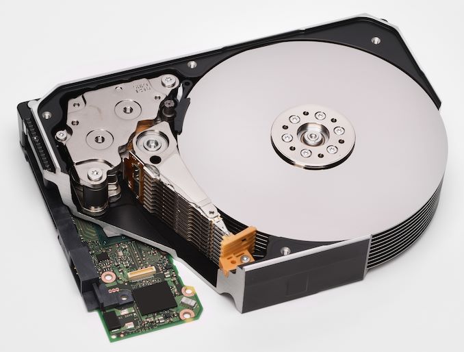
As Seagate ramps up shipments of its new heat assisted magnetic recording (HAMR)-based Mozaic 3+ hard drive platform, the company is both in the enviable position of shipping the first major new hard drive technology in a decade, and the much less enviable position of proving the reliability of the first major new hard drive technology in a decade. Due to HAMR's use of temporal heating with its platters, as well as all-new read/write heads, HAMR introduces multiple new changes at once that have raise questions about how reliable the technology will be. Looking to address these matters (and further promote their HAMR drives), Seagate has published a fresh blog post outlining the company's R&D efforts, and why the company expects their HAMR drives to last several years – as long or longer than current PMR hard drives.
According to the company, the reliability of Mozaic 3+ drives on par with traditional drives relying on perpendicular magnetic recording (PMR), the company says. In fact, components of HAMR HDDs have demonstrated a 50% increase in reliability over the past two years. Seagate says that Mozaic 3+ drives boast impressive durability metrics: their read/write heads have demonstrated capacity to handle over 3.2 petabytes of data transfer over 6,000 hours of operation, which exceeds data transfers of typical nearline hard drives by 20 times. Accordingly, Seagate is rating these drives for a mean time between failure (MTBF) 2.5 million hours, which is in-line with PMR-based drives.
Based on their field stress tests, involving over 500,000 Mozaic 3+ drives, Seagate says that the heads of Mozaic 3+ drives will last over seven years, surpassing the typical lifespan of current PMR-based drives. Generally, customers anticipate that modern PMR drives will last between four and five years with average usage, so these drives would exceed current expectations.
Altogether, Seagate is continuing aim for a seamless transition from PMR to HAMR drives in customer systems. That means ensuring that these new drives can fit into existing data center infrastructures without requiring any changes to enterprise specifications, warranty conditions, or form factors.
Storage
Across the internet, from online forums such as Reddit to various other tech media outlets, there's a lot of furor around reports of Intel's top-end 14th and 13th Gen K series of processors running into stability issues. As Intel's flagship chips, these parts come aggressively clocked in order to maximize performance through various implementations of boost and turbo, leaving them running close to their limits out of the box. But with high-end motherboards further goosing these chips to wring even more performance out of them, it would seem that the Intel desktop ecosystem has finally reached a tipping point where all of these efforts to boost performance have pushed these flagship chips to unstable conditions. To that end, Intel has released new gudiance to its consumer motherboard partners, strongly encouraging them to actually implment Intel's stock power settings, and to use those baseline settings as their out-of-the-box default.
While the underlying conditions are nothing new – we've published stories time and time again about motherboard features such as multi-core enhancement (MCE) and raised power consumption limits that seek to maximize how hard and how long systems are able to turbo boost – the issue has finally come to a head in the last couple of months thanks to accumulating reports of system instability with Intel's 13900K and 14900K processors. These instability problems are eventually solved by either tamping down on these motherboard performance-boosting features – bringing the chips back down to something closer to Intel's official operating parameters – or downclocking the chips entirely.
Intel first began publicly investigating the matter on the 27th of February, when Intel's Communications Manager, Thomas Hannaford, posted a thread on Intel's Community Product Support Forms titled "Regarding Reports of 13th/14th Gen Unlocked Desktop Users Experiencing Stability Issues". In this thread, Thomas Hannaford said, "Intel is aware of reports regarding Intel Core 13th and 14th Gen unlocked desktop processors experiencing issues with certain workloads. We're engaged with our partners and are conducting analysis of the reported issues. If you are experiencing these issues, please reach out to Intel Customer Support for further assistance in the interim."
Since that post went up, additional reports have been circulating about instability issues across various online forums and message boards. The underlying culprit has been theorized to be motherboards implementing an array of strategies to improve chip performance, including aggressive multi-core enhancement settings, "unlimited" PL2 turbo, and reduced load line calibration settings. At no point do any of these settings overclock a CPU and push it to a higher clockspeed than it's validated for, but these settings do everything possible to keep a chip at the highest clockspeed possible at all times – and in the process seem to have gone a step too far.
From "Why Intel Processors Draw More Power Than Expected: TDP and Turbo Explained"
We wrote a piece initially covering multi-core enhancement in 2012, detailing how motherboard manufacturers try to stay competitive with each other and leverage any headroom within the silicon to output the highest performance levels. And more recently, we've talked about how desktop systems with Intel chips are now regularly exceeding their rated TDPs – sometimes by extreme amounts – as motherboard vendors continue to push them to run as hard as possible for the best performance.
But things have changed since 2012. At the time, this wasn't so much of an issue, as overclocking was actually very favorable to increasing the performance of processors. But in 2024 with chips such as the Intel Core i9-14900K, we have CPUs shipping with a maximum turbo clock speed of 6.0 GHz and a peak power consumption of over 400 Watts, figures that were only a pipe dream a decade ago.
Jumping to the present time, over the weekend Intel released a statement about the matter to its partners, outlining their investigation so far and their sug... CPUs
While desktop PC power supplies receive the bulk of enthusiasts’ attention for good reasons – not the least of which being the vast selection of options that comes from being a standardized part – power supplies as a whole aren’t just a concern for big PCs. With the majority of PC sales having flipped to notebook sales some years ago, notebook power supplies already lead the market in volume. And while most laptops don’t need the kind of massively powered PSUs that dominate the desktop space, even that is slowly changing as desktop replacement-class laptops increasingly grow in performance and power consumption.
Perhaps the poster-child for the high-performance, high-powered laptop is Eurocom, who has a long history of developing heavy-duty DTR laptops that are all but portable desktop systems. Following recent trends in GPU power consumption and in GPU popularity for both gaming and AI workloads, the company has been selling a range of “mobile supercomputers”, which are practically large, tailor-made laptops that rival even the best of desktop computers – and have the power requirements to match.
In order to power their own high-end laptops, Eurocom has developed a rather unusual 780W AC adapter for high-performance laptops. Intended to power the most powerful of powerful laptops, their latest power adapter can supply over three-quarters of a kilowatt of DC power; a desktop-like wattage for a desktop-like device. It’s a laptop power adapter that’s unique in its scale, and with some room to scale up even further.
| Eurocom 780W AC Adapter Power specifications |
|
| RAIL | +20V |
| MAX OUTPUT | 39A |
| 780W | |
| DIMENSIONS | 325 x 110 x 40mm, 1.38kg |
| AC INPUT | 90 - 264 VAC, 50 - 60 Hz |
| MSRP | PSU: $299, Cable: $129+ |
Eurocom has offered this adapter for a few years now. But it’s taken on a new life as more laptops have been released that use such a large adapter (or two smaller 300W-ish power adapters). And, critically, Eurocom has made additional DC cable/connector sets for other manufactuers’ laptops, significantly increasing the number of systems it’s compatible with. Currently, Eurocom offers DC cables for the following laptops:
Externally, the Eurocom 780W AC adapter looks like a hybrid between a PC PSU and a laptop adapter. It is shaped like an oversized laptop AC adapter but has a metallic body and cooling vents/fans. Eurocom advertises that it weighs “only 1.34kg”, which is the weight of an entire 14-inch laptop by comparison, but is relatively lightweight for a PSU with that kind of power output. The company logo is debossed across the top side of the adapter, with four round anti-slip pads found at its bottom. Care needs to be taken while moving it around because the metallic edges and weight can spell trouble for wooden surfaces.
Eurocom installed a small information display on the AC adapter, which shows the current, voltage, and power output, as well as the temperature of the adapter. It is not perfectly accur... Cases/Cooling/PSUs

Seagate Technology has reportedly notified its customers abouts its plans to raise prices on new hard drive orders and for demands that exceed prior agreements, echoing a similar move by Western Digital, which increased its prices earlier this month. These changes come in response to a surge in demand for high-capacity HDDs and constraints in supply due to decreased production capabilities of both Seagate and Western Digital, reports TrendForce.
According to industry insights reported by TechNews, the sector anticipates that the scarcity of high-capacity HDD products will persist throughout the current quarter and possibly extend over the entire year. It is forecasted that HDD prices will rise by 5% to 10% in Q2 2024 alone and could increase further as a reault of the ongoing challenges faced by the storage industry.
The primary driver behind Seagate's decision is increased demand for high-capacity HDDs, which are used to train AI models. This demand spike, coupled with a reduction in production output from hard drive makers, has created a significant supply-demand imbalance. As a result, Seagate has decided to adjust their pricing strategy to manage the situation. Further exacerbating the issue are global inflationary pressures which continue to inflate costs across the board, which also contributed to the company's decision to increase prices, Seagate said in a message to clients published by TrendForce.
Seagate emphasized that its reduced production capacity has been a major challenge, hindering the company's ability to fulfill customer demands fully and promptly.
"As a result, we will be implementing price increases effective immediately on new orders and for demand that is over and above previously committed volumes," the alleged memo from Seagate reads. "Supply constraints are expected to continue and as such we anticipate that prices will continue to increase in the coming quarters."
Earlier this month Western Digital also informed its customers about price hikes for its HDD and SSD products. This notification was based on similar issues — higher than anticipated demand across the whole product range and additional supply chain challenges affecting the electronics sector. Western Digital's announcement made it clear that these disruptions are likely to continue, prompting further price adjustments.
Sources: TrendForce, TrendForce, TechNews
Storage
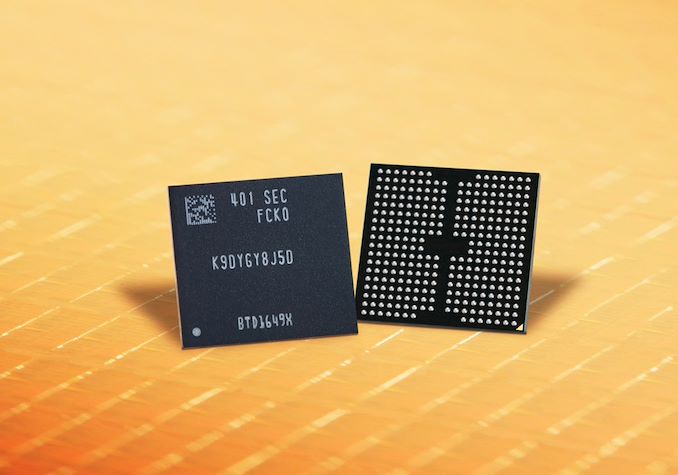
Samsung Electronics has started mass production of its 9th generation of V-NAND memory. The first dies based on their latest NAND tech come in a 1 Tb capacity using a triple-level cell (TLC) architecture, with data transfer rates as high as 3.2 GT/s. The new 3D TLC NAND memory will initially be used to build high-capacity and high-performance SSDs, which will help to solidify Samsung's position in the storage market.
Diving right in, Samsung is conspicuously avoiding to list the number of layers in their latest generation NAND, which is the principle driving factor in increasing capacity generation-on-generation. The company's current 8th gen V-NAND is 236 layers – similar to its major competitors – and word on the street is that 9th gen V-NAND ups that to 290 layers, though this remains to be confirmed.
Regardless, Samsung says that its 9th generation V-NAND memory boasts an approximate 50% improvement in bit density over its 8th generation predecessor. Driving this gains, the company cites the miniaturization of the cell size, as well as the integration of enhanced memory cell technologies that reduce interference and extend the lifespan of the cells. With their latest NAND technology, Samsung has also been able to eliminate dummy channel holes, thus reducing the planar area of the memory cells.
Interestingly, today's announcement also marks the first time that Samsung has publicly confirmed their use of string stacking in their NAND, referring to it as their "double-stack structure." The company is widely believed to have been using sting stacking back in their 8th generation NAND as well, however this was never confirmed by the company. Regardless, the use of string stacking is only going to increase from here, as vendors look to keep adding layers to their NAND dies, while manufacturing variability and channel hole tolerances make it difficult to produce more than 150-200 layers in a single stack.
| Samsung TLC V- NAND Flash Memory | ||
| 9th Gen V-NAND | 8th Gen V-NAND | |
| Layers | 290? | 236 |
| Decks | 2 (x145) | 2 (x118) |
| Die Capacity | 1 Tbit | 1 Tbit |
| Die Size (mm2) | ?mm2 | ?mm2 |
| Density (Gbit/mm2) | ? | ? |
| I/O Speed | 3.2 GT/s (Toggle 5.1) |
2.4 GT/s (Toggle 5.0) |
| Planes | 6? | 4 |
| CuA / PuC | Yes | Yes |
Speaking of channel holes, another key technological enhancement in the 9th gen V-NAND is Samsung's advanced 'channel hole etching' technology. This process improves manufacturing productivity by enabling the simultaneous creation of electron pathways within a double-stack structure. This method is crucial as it enables efficient drilling through more layers, which is increasingly important as cell layers are added.
The latest V-NAND also features the introduction of a faster NAND flash interface, Toggle DDR 5.1, which boosts peak data transfer rates by 33% to 3.2 GT/s, or almost 400MB/sec for a single die. Additionally, 9th gen V-NAND's power consumption has been reduced by 10%, according to Samsung. Though Samsung doesn't state under what conditions – presumably, this is at iso-frequency rather than max frequency.
Samsung's launch of 1Tb TLC V-NAND is set to be followed by the release of a quad-level cell (QLC) model later this year.
"We are excited to deliver the industry’s first 9th-gen V-NAND which will bring future... SSDs
As Qualcomm prepares for the mid-year launch of their forthcoming Snapdragon X SoCs for PCs, and the eagerly anticipated Oryon CPU cores within, the company is finally shoring up their official product plans, and releasing some additional technical details in the process. Thus far the company has been demonstrating their Snapdragon X Elite SoC in its highest-performing, fully-enabled configuration. But the retail Snapdragon X Elite will not be a single part; instead, Qualcomm is preparing a whole range of chip configurations for various price/performance tiers in the market. Altogether, there will be 3 Snapdragon X Elite SKUs that differ in CPU and GPU performance.
As well, the company is introducing a second Snapdragon X tier, Snapdragon X Plus, for those SKUs positioned below the Elite performance tier. As of today, this will be a single configuration. But if the Snapdragon X lineup is successful and demand warrants it, I would not be surprised to see Qualcomm expand it further – as they have certainly left themselves the room for it in their product stack. In the meantime, with Qualcomm’s expected launch competition now shipping (Intel Core Ultra Meteor Lake and AMD Ryzen Mobile 8040 Hawk Point), the company is also very confident that even these reduced performance Snapdragon X Plus chips will be able to beat Intel and AMD in multithreaded performance – never mind the top-tier Snapdragon X Elite chips.
Qualcomm will be launching this expanded four chip stack at once; so both Snapdragon X Elite and Snapdragon X Plus tier devices should be available at the same time. The company’s goal is still to have devices on the shelf “mid-year”, although the company isn’t providing any more precise guidance than that. With Qualcomm’s CEO, Cristiano Amon, set to deliver a Computex keynote in June, I expect we’ll get more specific details on timings then, along with the company and its partners using the event to announce and showcase some retail laptop designs. So this is very much looking like a summer launch at the moment.
In the meantime, Qualcomm is already showing off what their Snapdragon X Plus chips can do with a fresh set of live benchmarks, akin to their Snapdragon X Elite performance previews from October 2023. We’ll dive into those in a bit, but suffice it to say, Qualcomm knows the score, and they want to make sure the entire world knows when they’re winning.
CPUs
As Seagate ramps up shipments of its new heat assisted magnetic recording (HAMR)-based Mozaic 3+ hard drive platform, the company is both in the enviable position of shipping the first major new hard drive technology in a decade, and the much less enviable position of proving the reliability of the first major new hard drive technology in a decade. Due to HAMR's use of temporal heating with its platters, as well as all-new read/write heads, HAMR introduces multiple new changes at once that have raise questions about how reliable the technology will be. Looking to address these matters (and further promote their HAMR drives), Seagate has published a fresh blog post outlining the company's R&D efforts, and why the company expects their HAMR drives to last several years – as long or longer than current PMR hard drives.
According to the company, the reliability of Mozaic 3+ drives on par with traditional drives relying on perpendicular magnetic recording (PMR), the company says. In fact, components of HAMR HDDs have demonstrated a 50% increase in reliability over the past two years. Seagate says that Mozaic 3+ drives boast impressive durability metrics: their read/write heads have demonstrated capacity to handle over 3.2 petabytes of data transfer over 6,000 hours of operation, which exceeds data transfers of typical nearline hard drives by 20 times. Accordingly, Seagate is rating these drives for a mean time between failure (MTBF) 2.5 million hours, which is in-line with PMR-based drives.
Based on their field stress tests, involving over 500,000 Mozaic 3+ drives, Seagate says that the heads of Mozaic 3+ drives will last over seven years, surpassing the typical lifespan of current PMR-based drives. Generally, customers anticipate that modern PMR drives will last between four and five years with average usage, so these drives would exceed current expectations.
Altogether, Seagate is continuing aim for a seamless transition from PMR to HAMR drives in customer systems. That means ensuring that these new drives can fit into existing data center infrastructures without requiring any changes to enterprise specifications, warranty conditions, or form factors.
Storage
With the arrival of spring comes showers, flowers, and in the technology industry, TSMC's annual technology symposium series. With customers spread all around the world, the Taiwanese pure play foundry has adopted an interesting strategy for updating its customers on its fab plans, holding a series of symposiums from Silicon Valley to Shanghai. Kicking off the series every year – and giving us our first real look at TSMC's updated foundry plans for the coming years – is the Santa Clara stop, where yesterday the company has detailed several new technologies, ranging from more advanced lithography processes to massive, wafer-scale chip packing options.
Today we're publishing several stories based on TSMC's different offerings, starting with TSMC's marquee announcement: their A16 process node. Meanwhile, for the rest of our symposium stories, please be sure to check out the related reading below, and check back for additional stories.
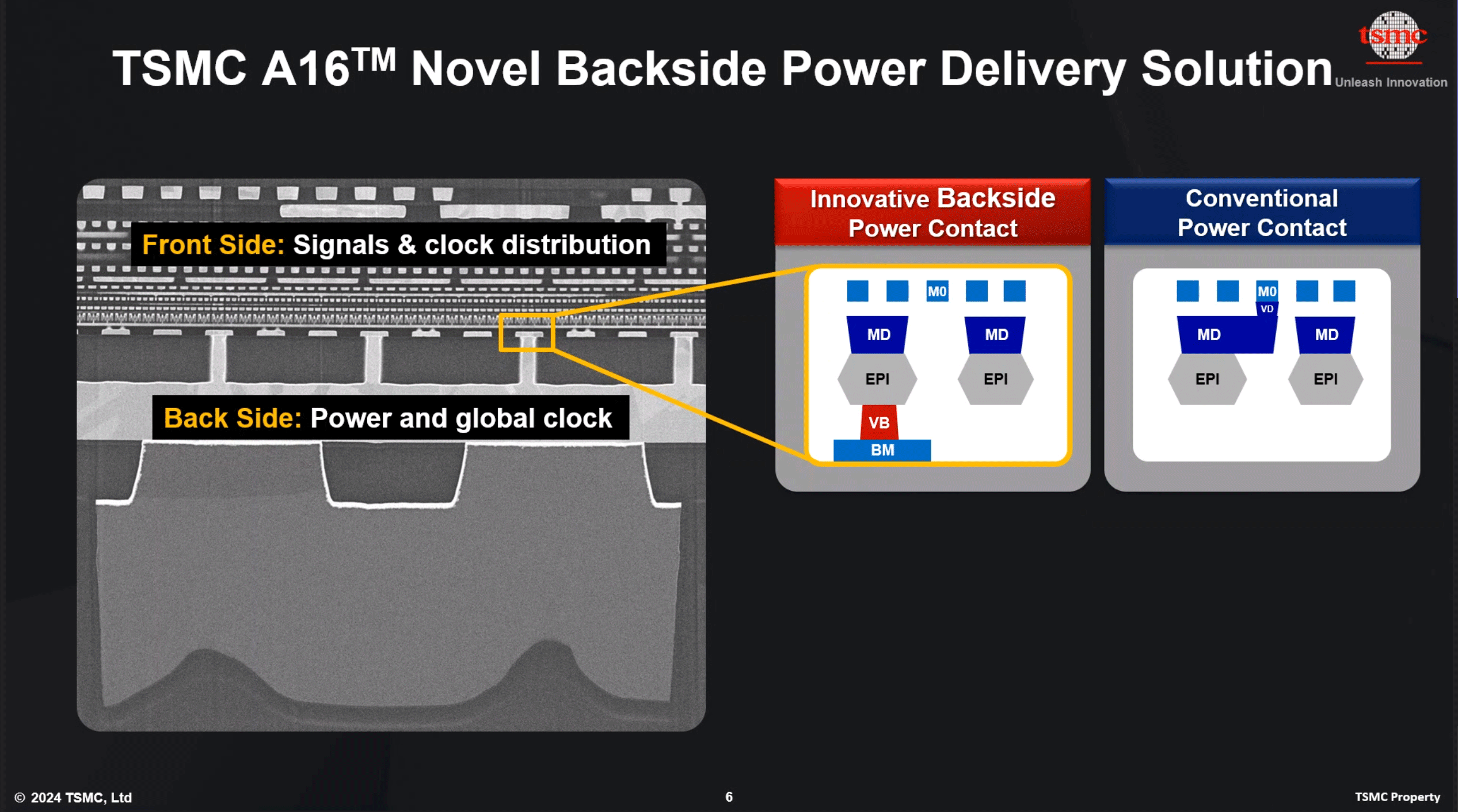
Headlining its Silicon Valley stop, TSMC announced its first 'angstrom-class' process technology: A16. Following a production schedule shift that has seen backside power delivery network technology (BSPDN) removed from TSMC's N2P node, the new 1.6nm-class production node will now be the first process to introduce BSPDN to TSMC's chipmaking repertoire. With the addition of backside power capabilities and other improvements, TSMC expects A16 to offer significantly improved performance and energy efficiency compared to TSMC's N2P fabrication process. It will be available to TSMC's clients starting H2 2026.
At a high level, TSMC's A16 process technology will rely on gate-all-around (GAAFET) nanosheet transistors and will feature a backside power rail, which will both improve power delivery and moderately increase transistor density. Compared to TSMC's N2P fabrication process, A16 is expected to offer a performance improvement of 8% to 10% at the same voltage and complexity, or a 15% to 20% reduction in power consumption at the same frequency and transistor count. TSMC is not listing detailed density parameters this far out, but the company says that chip density will increase by 1.07x to 1.10x – keeping in mind that transistor density heavily depends on the type and libraries of transistors used.
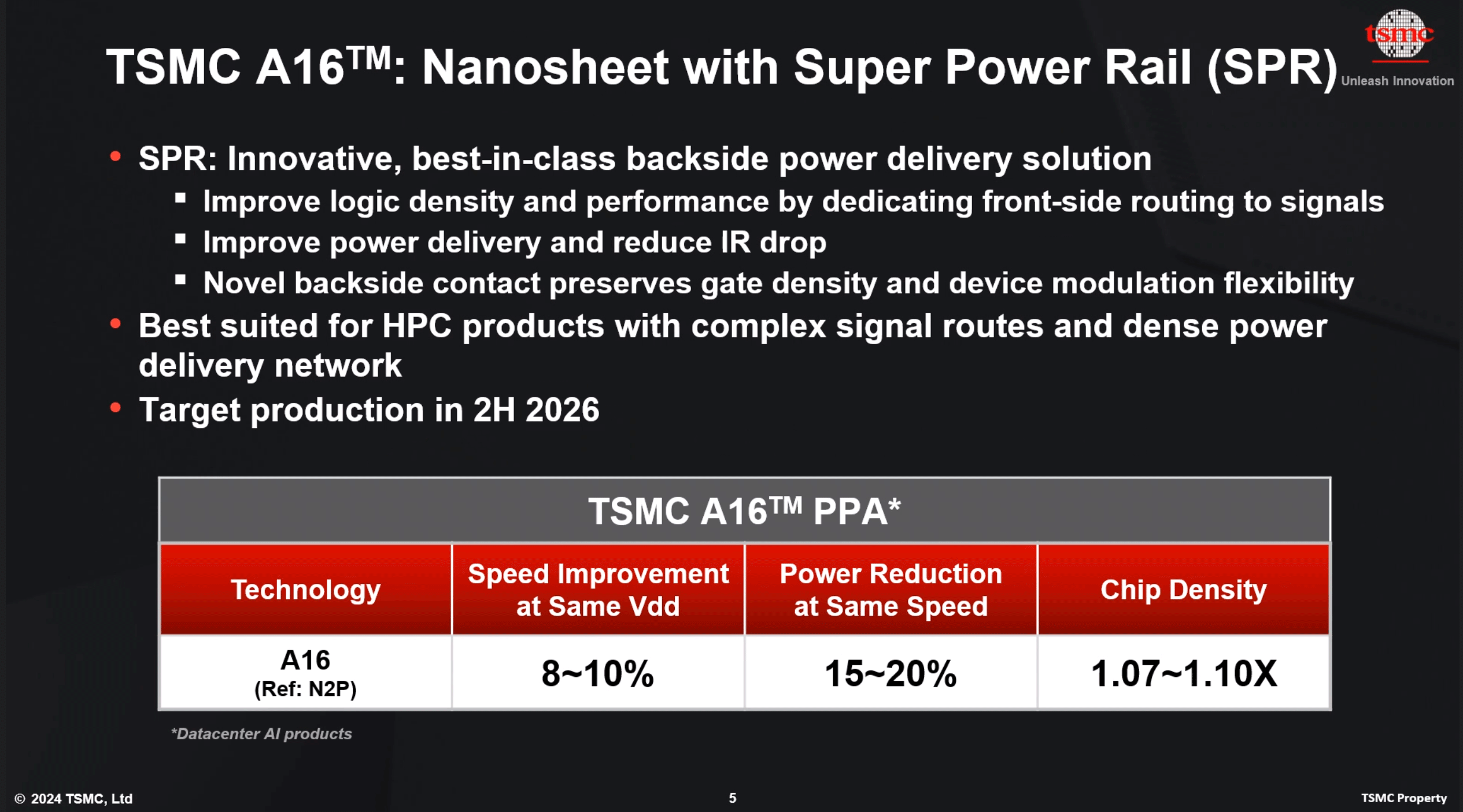
The key innovation of TSMC's A16 node, is its Super Power Rail (SPR) backside power delivery network, a first for TSMC. The contract chipmaker claims that A16's SPR is specifically tailored for high-performance computing products that feature both complex signal routes and dense power circuitry.
As noted earlier, with this week's announcement, A16 has now become the launch vehicle for backside power delivery at TSMC. The company was initially slated to offer BSPDN technology with N2P in 2026, but for reasons that aren't entirely clear, the tech has been punted from N2P and moved to A16. TSMC's official timing for N2P in 2023 was always a bit loose, so it's hard to say if this represents much of a practical delay for BSPDN at TSMC. But at the same time, it's important to underscore that A16 isn't just N2P renamed, but rather it will be a di... Semiconductors
Seagate Technology has reportedly notified its customers abouts its plans to raise prices on new hard drive orders and for demands that exceed prior agreements, echoing a similar move by Western Digital, which increased its prices earlier this month. These changes come in response to a surge in demand for high-capacity HDDs and constraints in supply due to decreased production capabilities of both Seagate and Western Digital, reports TrendForce.
According to industry insights reported by TechNews, the sector anticipates that the scarcity of high-capacity HDD products will persist throughout the current quarter and possibly extend over the entire year. It is forecasted that HDD prices will rise by 5% to 10% in Q2 2024 alone and could increase further as a reault of the ongoing challenges faced by the storage industry.
The primary driver behind Seagate's decision is increased demand for high-capacity HDDs, which are used to train AI models. This demand spike, coupled with a reduction in production output from hard drive makers, has created a significant supply-demand imbalance. As a result, Seagate has decided to adjust their pricing strategy to manage the situation. Further exacerbating the issue are global inflationary pressures which continue to inflate costs across the board, which also contributed to the company's decision to increase prices, Seagate said in a message to clients published by TrendForce.
Seagate emphasized that its reduced production capacity has been a major challenge, hindering the company's ability to fulfill customer demands fully and promptly.
"As a result, we will be implementing price increases effective immediately on new orders and for demand that is over and above previously committed volumes," the alleged memo from Seagate reads. "Supply constraints are expected to continue and as such we anticipate that prices will continue to increase in the coming quarters."
Earlier this month Western Digital also informed its customers about price hikes for its HDD and SSD products. This notification was based on similar issues — higher than anticipated demand across the whole product range and additional supply chain challenges affecting the electronics sector. Western Digital's announcement made it clear that these disruptions are likely to continue, prompting further price adjustments.
Sources: TrendForce, TrendForce, TechNews
Storage
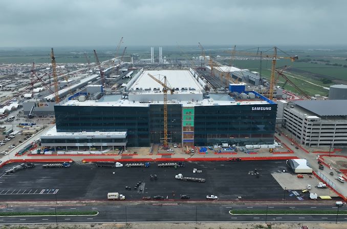
Samsung Electronics this week was awarded up to $6.4 billion from the U.S. government under the CHIPS and Science Act to build its new fab complex in Taylor, Texas. This is the third major award under the act in the last month, with all three leading-edge fabs – Intel, TSMC, and now Samsung – receiving multi-billion dollar funding packages under the domestic chip production program. Overall, the final price tag on Samsung's new fab complex is expected to reach $40 billion by the time it's completed later this decade.
Samsung's CHIPS Act funding was announced during a celebratory event attended by U.S. Secretary of Commerce Gina Raimondo and Samsung Semiconductor chief executive Kye Hyun Kyung. During the event, Kyung outlined the strategic goals of the expansion, emphasizing that the additional funding will not only increase production capacity but also strengthen the entire local semiconductor ecosystem. Samsung plans to equip its fab near Taylor, Texas, with the latest wafer fab tools to produce advanced chips. The Financial Times reports that Samsung aims to produce semiconductors on its 2nm-class process technology starting 2026, though for now this is unofficial information.
"I am pleased to announce a preliminary agreement between Samsung and the Department of Commerce to bring Samsung's advanced semiconductor manufacturing and research and development to Texas," said Joe Biden, the U.S. president, in a statement. "This announcement will unleash over $40 billion in investment from Samsung, and cement central Texas's role as a state-of-the-art semiconductor ecosystem, creating at least 21,500 jobs and leveraging up to $40 million in CHIPS funding to train and develop the local workforce. These facilities will support the production of some of the most powerful chips in the world, which are essential to advanced technologies like artificial intelligence and will bolster U.S. national security."
Samsung has been a significant contributor to the Texas economy for decades, starting chip manufacturing in the U.S. in 1996. With previous investments totaling $18 billion in its Austin operations, Samsung's expansion into Taylor with an additional investment of at least $17 billion underscores its role as one of the largest foreign direct investors in U.S. history. The total expected investment in the new fab surpasses $40 billion, making it one of the largest for a greenfield project in the nation and transforming Taylor into a major hub for semiconductor manufacturing.
The CEO highlighted the substantial economic impact of Samsung's operations, noting a nearly double increase in regional economic output from $13.6 billion to $26.8 billion between 2022 and 2023. The ongoing expansion is projected to further stimulate economic growth, create thousands of jobs, and enhance the community's overall development.
“We are not just expanding production facilities; we’re strengthening the local semiconductor ecosystem and positioning the U.S. as a global semiconductor manufacturing destination.” said Kyung. “To meet the expected surge in demand from U.S. customers, for future products like AI chips, our fabs will be equipped for cutting-edge process technologies and help bring security to the U.S. semiconductor supply chain.”
Samsung is also committed to environmental sustainability and workforce development. The company plans to operate using 100% clean energy and incorporate advanced water management technologies. Additionally, it is investing in education and training programs to develop a new generation of semiconductor professionals. These initiatives include partnerships with educational institutions and programs tailored for military veterans.
In his remarks, Kyung expressed gratitude to President Biden, Secretary Raimondo, and other governmental and community supporters for their ongoing support. This collaborative effort between Samsung and various levels of government, as well as the local community, is pivotal in advancing America's... Semiconductors
AMD has recently expanded its Ryzen 8000 series by introducing the Ryzen 7 8700F and Ryzen 5 8400F processors. Initially launched in China, these chips were added to AMD's global website, signaling they are available worldwide, apparently from April 1st. Built from the recent Zen 4-based Phoenix APUs using the TSMC 4nm node as their Zen 4 mobile chips, these new CPUs lack integrated graphics. However, the Ryzen 7 8700F does include the integrated Ryzen AI NPU for added capabilities in a world currently dominated by AI and moving it directly into the PC.
The company's decision to announce these chips in China aligns with its strategy to offer Ryzen solutions at every price point in the market. Although AMD didn't initially disclose the full specifications of these F-series models, and we did reach out to the company to ask about them, they refused to discuss them with us. Their listing on the website has now been updated with a complete list of specifications and features, with everything but the price mentioned.
| AMD Ryzen 8000G vs. Ryzen 8000F Series (Desktop) Zen 4 (Phoenix) |
|||||||||
| AnandTech | Cores/Threads | Base Freq |
Turbo Freq |
GPU | GPU Freq |
Ryzen AI (NPU) |
L3 Cache (MB) |
TDP | MSRP |
| Ryzen 7 | |||||||||
| Ryzen 7 8700G | 8/16 | 4200 | 5100 | R780M 12 CUs |
2900 | Y | 16 | 65W | $329 |
| Ryzen 7 8700F | 8/16 | 4100 | 5000 | - | - | Y | 16 | 65W | ? |
| Ryzen 5 | |||||||||
| Ryzen 5 8600G | 6/12 | 4300 | 5000 | R760M 8 CUs |
2800 | Y | 16 | 65W | $229 |
| Ryzen 5 8400F | 6/12 | 4200 | 4700 | - | - | N | 16 | 65W | ? |
The Ryzen 7 8700F features an 8C/16T design, with 16MB of L3 cache and the same 65W TDP as the Ryzen 7 8700G. Although the base clock speed is 4.1 GHz, it boosts to 5.0 GHz; this is 100 MHz less on both base/boost clocks than the 8700G. Meanwhile, the Ryzen 5 8400F is a slightly scaled-down version of the Ryzen 8600G APU, with 6C/12, 16MB of L3 cache, and again has a 100 MHz reduction to base clocks compared to the 8600G. Unlike the Ryzen 5 8400F, the Ryzen 7 8700F keeps AMD's Ryzen AI NPU, adding additional capability for generative AI.
The Ryzen 5 8400F can boost up to 4.7 GHz, 300 MHz slower than the Ryzen 5 8600G. AMD also allows overclocking for these new F-series chips, which means users could potentially boost the performance of these processors to match their G-series equivalents.
Pricing details are still pending, but to remain competitive, AMD will likely need to price these CPUs below the 8700G and 8600G, as well as the Ryzen 7 7700 and Ryzen 5 7600. These CPUs offer, albeit very limited, integrated graphics and have double the L3 cache capacity, along with higher boost clocks than the 8000F series chips, so pricing is something to consider whenever pricing becomes available.
CPUs
Corsair has introduced a family of registered memory modules with ECC that are designed for AMD's Ryzen Threadripper 7000 and Intel's Xeon W-2400/3400-series processors. The new Corsair WS DDR5 RDIMMs with AMD EXPO and Intel XMP 3.0 profiles will be available in kits of up to 256 GB capacity and at speeds of up to 6400 MT/s.
Corsair's family of WS DDR5 RDIMMs includes 16 GB modules operating at up to 6400 MT/s with CL32 latency as well as 32 GB modules functioning at 5600 MT/s with CL40 latency. At present, Corsair offers a quad-channel 64 GB kit (4×16GB, up to 6400 MT/s), a quad-channel 128GB kit (4×32GB, 5600 MT/s), an eight-channel 128 GB kit (8×16GB, 5600 MT/s), and an eight-channel 256 GB kit (8×32GB, 5600 MT/s) and it remains to be seen whether the company will expand the lineup.
Corsair's WS DDR5 RDIMMs are designed for AMD's TRX50 and WRX90 platforms as well as Intel's W790 platform and are therefore compatible with AMD's Ryzen Threadripper Pro 7000 and 7000WX-series as well as Intel's Xeon W-2400/3400-series CPUs. The modules feature both AMD EXPO and Intel XMP 3.0 profiles to easily set their beyond-JEDEC-spec settings and come with thin heat spreaders made of pyrolytic graphite sheet (PGS), which thermal conductivity than that of copper and aluminum of the same thickness. For now, Corsair does not disclose which RCD and memory chips its registered memory modules use.
Unlike many of its rivals among leading DIMM manufacturers, Corsair did not introduce its enthusiast-grade RDIMMs when AMD and Intel released their Ryzen Threadripper and Xeon W-series platforms for extreme workstations last year. It is hard to tell what the reason for that is, but perhaps the company wanted to gain experience working with modules featuring registered clock drivers (RCDs) as well as AMD's and Intel's platforms for extreme workstations.
The result of the delay looks to be quite rewarding: unlike modules from its competitors that either feature AMD EXPO or Intel XMP 3.0 profiles, Corsair's WS DDR5 RDIMMs come with both. While this may not be important on the DIY market where people know exactly what they are buying for their platform, this is a great feature for system integrators, which can use Corsair WS DDR5 RDIMMs both for their AMD Ryzen Threadripper and Intel Xeon W-series builds, something that greatly simplifies their inventory management.
Since Corsair's WS DDR5 RDIMMs are aimed at workstations and are tested to offer reliable performance beyond JEDEC specifications, they are quite expensive. The cheapest 64 GB DDR5-5600 CL40 kit costs $450, the fastest 64 GB DDR5-6400 CL32 kit is priced at $460, whereas the highest end 256 GB DDR5-5600 CL40 kit is priced at $1,290.
Memory
Across the internet, from online forums such as Reddit to various other tech media outlets, there's a lot of furor around reports of Intel's top-end 14th and 13th Gen K series of processors running into stability issues. As Intel's flagship chips, these parts come aggressively clocked in order to maximize performance through various implementations of boost and turbo, leaving them running close to their limits out of the box. But with high-end motherboards further goosing these chips to wring even more performance out of them, it would seem that the Intel desktop ecosystem has finally reached a tipping point where all of these efforts to boost performance have pushed these flagship chips to unstable conditions. To that end, Intel has released new gudiance to its consumer motherboard partners, strongly encouraging them to actually implment Intel's stock power settings, and to use those baseline settings as their out-of-the-box default.
While the underlying conditions are nothing new – we've published stories time and time again about motherboard features such as multi-core enhancement (MCE) and raised power consumption limits that seek to maximize how hard and how long systems are able to turbo boost – the issue has finally come to a head in the last couple of months thanks to accumulating reports of system instability with Intel's 13900K and 14900K processors. These instability problems are eventually solved by either tamping down on these motherboard performance-boosting features – bringing the chips back down to something closer to Intel's official operating parameters – or downclocking the chips entirely.
Intel first began publicly investigating the matter on the 27th of February, when Intel's Communications Manager, Thomas Hannaford, posted a thread on Intel's Community Product Support Forms titled "Regarding Reports of 13th/14th Gen Unlocked Desktop Users Experiencing Stability Issues". In this thread, Thomas Hannaford said, "Intel is aware of reports regarding Intel Core 13th and 14th Gen unlocked desktop processors experiencing issues with certain workloads. We're engaged with our partners and are conducting analysis of the reported issues. If you are experiencing these issues, please reach out to Intel Customer Support for further assistance in the interim."
Since that post went up, additional reports have been circulating about instability issues across various online forums and message boards. The underlying culprit has been theorized to be motherboards implementing an array of strategies to improve chip performance, including aggressive multi-core enhancement settings, "unlimited" PL2 turbo, and reduced load line calibration settings. At no point do any of these settings overclock a CPU and push it to a higher clockspeed than it's validated for, but these settings do everything possible to keep a chip at the highest clockspeed possible at all times – and in the process seem to have gone a step too far.
From "Why Intel Processors Draw More Power Than Expected: TDP and Turbo Explained"
We wrote a piece initially covering multi-core enhancement in 2012, detailing how motherboard manufacturers try to stay competitive with each other and leverage any headroom within the silicon to output the highest performance levels. And more recently, we've talked about how desktop systems with Intel chips are now regularly exceeding their rated TDPs – sometimes by extreme amounts – as motherboard vendors continue to push them to run as hard as possible for the best performance.
But things have changed since 2012. At the time, this wasn't so much of an issue, as overclocking was actually very favorable to increasing the performance of processors. But in 2024 with chips such as the Intel Core i9-14900K, we have CPUs shipping with a maximum turbo clock speed of 6.0 GHz and a peak power consumption of over 400 Watts, figures that were only a pipe dream a decade ago.
Jumping to the present time, over the weekend Intel released a statement about the matter to its partners, outlining their investigation so far and their sug... CPUs


Optical connectivity – and especially silicon photonics – is expected to become a crucial technology to enable connectivity for next-generation datacenters, particularly those designed HPC applications. With ever-increasing bandwidth requirements needed to keep up with (and keep scaling out) system performance, copper signaling alone won't be enough to keep up. To that end, several companies are developing silicon photonics solutions, including fab providers like TSMC, who this week outlined its 3D Optical Engine roadmap as part of its 2024 North American Technology Symposium, laying out its plan to bring up to 12.8 Tbps optical connectivity to TSMC-fabbed processors.
TSMC's Compact Universal Photonic Engine (COUPE) stacks an electronics integrated circuit on photonic integrated circuit (EIC-on-PIC) using the company's SoIC-X packaging technology. The foundry says that usage of its SoIC-X enables the lowest impedance at the die-to-die interface and therefore the highest energy efficiency. The EIC itself is produced at a 65nm-class process technology.
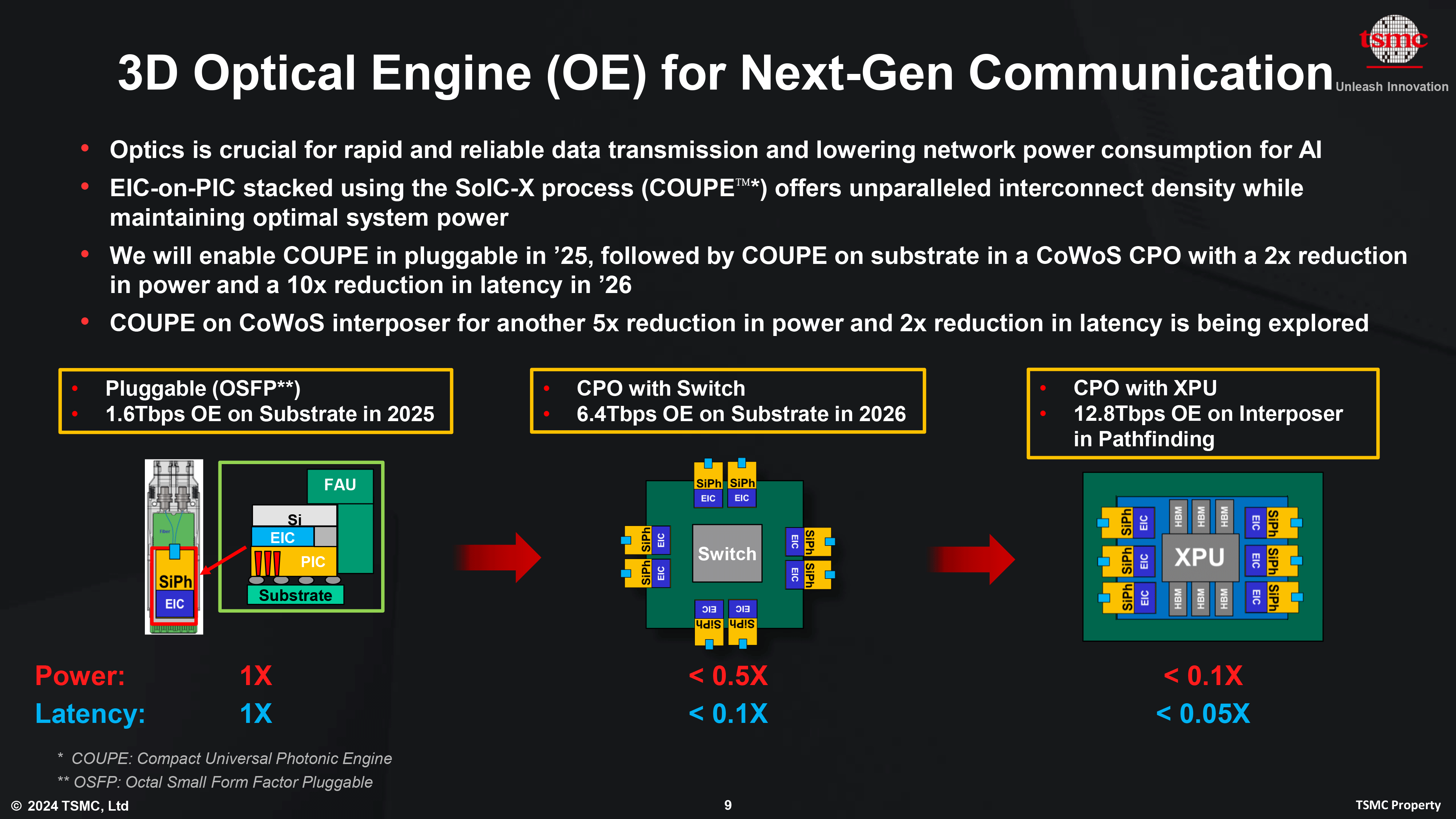
TSMC's 1st Generation 3D Optical Engine (or COUPE) will be integrated into an OSFP pluggable device running at 1.6 Tbps. That's a transfer rate well ahead of current copper Ethernet standards – which top out at 800 Gbps – underscoring the immediate bandwidth advantage of optical interconnects for heavily-networked compute clusters, never mind the expected power savings.
Looking further ahead, the 2nd Generation of COUPE is designed to integrate into CoWoS packaging as co-packaged optics with a switch, allowing optical interconnections to be brought to the motherboard level. This version COUPE will support data transfer rates of up to 6.40 Tbps with reduced latency compared to the first version.
TSMC's third iteration of COUPE – COUPE running on a CoWoS interposer – is projected to improve on things one step further, increasing transfer rates to 12.8 Tbps while bringing optical connectivity even closer to the processor itself. At present, COUPE-on-CoWoS is in the pathfinding stage of development and TSMC does not have a target date set.
Ultimately, unlike many of its industry peers, TSMC has not participated in the silicon photonics market up until now, leaving this to players like GlobalFoundries. But with its 3D Optical Engine Strategy, the company will enter this important market as it looks to make up for lost time.
As Seagate ramps up shipments of its new heat assisted magnetic recording (HAMR)-based Mozaic 3+ hard drive platform, the company is both in the enviable position of shipping the first major new hard drive technology in a decade, and the much less enviable position of proving the reliability of the first major new hard drive technology in a decade. Due to HAMR's use of temporal heating with its platters, as well as all-new read/write heads, HAMR introduces multiple new changes at once that have raise questions about how reliable the technology will be. Looking to address these matters (and further promote their HAMR drives), Seagate has published a fresh blog post outlining the company's R&D efforts, and why the company expects their HAMR drives to last several years – as long or longer than current PMR hard drives.
According to the company, the reliability of Mozaic 3+ drives on par with traditional drives relying on perpendicular magnetic recording (PMR), the company says. In fact, components of HAMR HDDs have demonstrated a 50% increase in reliability over the past two years. Seagate says that Mozaic 3+ drives boast impressive durability metrics: their read/write heads have demonstrated capacity to handle over 3.2 petabytes of data transfer over 6,000 hours of operation, which exceeds data transfers of typical nearline hard drives by 20 times. Accordingly, Seagate is rating these drives for a mean time between failure (MTBF) 2.5 million hours, which is in-line with PMR-based drives.
Based on their field stress tests, involving over 500,000 Mozaic 3+ drives, Seagate says that the heads of Mozaic 3+ drives will last over seven years, surpassing the typical lifespan of current PMR-based drives. Generally, customers anticipate that modern PMR drives will last between four and five years with average usage, so these drives would exceed current expectations.
Altogether, Seagate is continuing aim for a seamless transition from PMR to HAMR drives in customer systems. That means ensuring that these new drives can fit into existing data center infrastructures without requiring any changes to enterprise specifications, warranty conditions, or form factors.
Storage
Optical connectivity – and especially silicon photonics – is expected to become a crucial technology to enable connectivity for next-generation datacenters, particularly those designed HPC applications. With ever-increasing bandwidth requirements needed to keep up with (and keep scaling out) system performance, copper signaling alone won't be enough to keep up. To that end, several companies are developing silicon photonics solutions, including fab providers like TSMC, who this week outlined its 3D Optical Engine roadmap as part of its 2024 North American Technology Symposium, laying out its plan to bring up to 12.8 Tbps optical connectivity to TSMC-fabbed processors.
TSMC's Compact Universal Photonic Engine (COUPE) stacks an electronics integrated circuit on photonic integrated circuit (EIC-on-PIC) using the company's SoIC-X packaging technology. The foundry says that usage of its SoIC-X enables the lowest impedance at the die-to-die interface and therefore the highest energy efficiency. The EIC itself is produced at a 65nm-class process technology.
TSMC's 1st Generation 3D Optical Engine (or COUPE) will be integrated into an OSFP pluggable device running at 1.6 Tbps. That's a transfer rate well ahead of current copper Ethernet standards – which top out at 800 Gbps – underscoring the immediate bandwidth advantage of optical interconnects for heavily-networked compute clusters, never mind the expected power savings.
Looking further ahead, the 2nd Generation of COUPE is designed to integrate into CoWoS packaging as co-packaged optics with a switch, allowing optical interconnections to be brought to the motherboard level. This version COUPE will support data transfer rates of up to 6.40 Tbps with reduced latency compared to the first version.
TSMC's third iteration of COUPE – COUPE running on a CoWoS interposer – is projected to improve on things one step further, increasing transfer rates to 12.8 Tbps while bringing optical connectivity even closer to the processor itself. At present, COUPE-on-CoWoS is in the pathfinding stage of development and TSMC does not have a target date set.
Ultimately, unlike many of its industry peers, TSMC has not participated in the silicon photonics market up until now, leaving this to players like GlobalFoundries. But with its 3D Optical Engine Strategy, the company will enter this important market as it looks to make up for lost time.

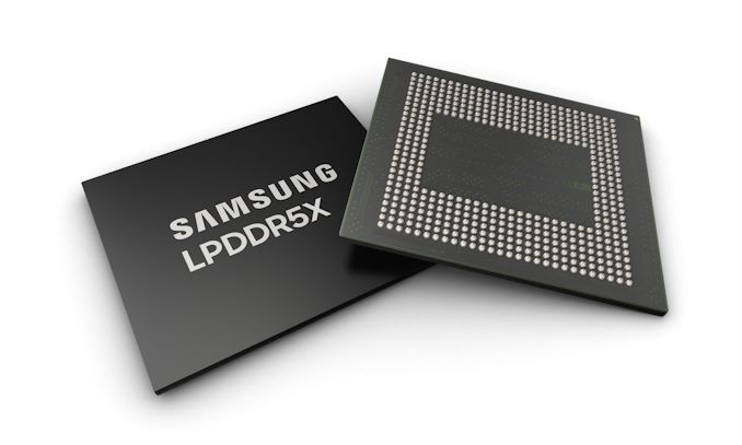
Samsung today has announced that they have developed an even faster generation of LPDDR5X memory that is set to top out at LPDDR5X-10700 speeds. The updated memory is slated to offer 25% better performance and 30% greater capacity compared to existing mobile DRAM devices from the company. The new chips also appear to be tangibly faster than Micron's LPDDR5X memory and SK hynix's LPDDR5T chips.
Samsung's forthcoming LPDDR5X devices feature a data transfer rate of 10.7 GT/s as well as maximum capacity per stack of 32 GB. This allows Samsung's clients to equip their latest smartphones or laptops with 32 GB of low-power memory using just one DRAM package, which greatly simplifies their designs. Samsung says that 32 GB of memory will be particularly beneficial for on-device AI applications.
Samsung is using its latest-generation 12nm-class DRAM process technology to make its LPDDR5X-10700 devices, which allows the company to achieve the smallest LPDDR device size in the industry, the memory maker said.
In terms of power efficiency, Samsung claims that they have integrated multiple new power-saving features into the new LPDDR5X devices. These include an optimized power variation system that adjusts energy consumption based on workload, and expanded intervals for low-power mode that extend the periods of energy saving. These innovations collectively enhance power efficiency by 25% compared to earlier versions, benefiting mobile platforms by extending battery life, the company said.
“As demand for low-power, high-performance memory increases, LPDDR DRAM is expected to expand its applications from mainly mobile to other areas that traditionally require higher performance and reliability such as PCs, accelerators, servers and automobiles,” said YongCheol Bae, Executive Vice President of Memory Product Planning of the Memory Business at Samsung Electronics. “Samsung will continue to innovate and deliver optimized products for the upcoming on-device AI era through close collaboration with customers.”
Samsung plans to initiate mass production of the 10.7 GT/s LPDDR5X DRAM in the second half of this year. This follows a series of compatibility tests with mobile application processors and device manufacturers to ensure seamless integration into future products.
DRAM
With the arrival of spring comes showers, flowers, and in the technology industry, TSMC's annual technology symposium series. With customers spread all around the world, the Taiwanese pure play foundry has adopted an interesting strategy for updating its customers on its fab plans, holding a series of symposiums from Silicon Valley to Shanghai. Kicking off the series every year – and giving us our first real look at TSMC's updated foundry plans for the coming years – is the Santa Clara stop, where yesterday the company has detailed several new technologies, ranging from more advanced lithography processes to massive, wafer-scale chip packing options.
Today we're publishing several stories based on TSMC's different offerings, starting with TSMC's marquee announcement: their A16 process node. Meanwhile, for the rest of our symposium stories, please be sure to check out the related reading below, and check back for additional stories.
Headlining its Silicon Valley stop, TSMC announced its first 'angstrom-class' process technology: A16. Following a production schedule shift that has seen backside power delivery network technology (BSPDN) removed from TSMC's N2P node, the new 1.6nm-class production node will now be the first process to introduce BSPDN to TSMC's chipmaking repertoire. With the addition of backside power capabilities and other improvements, TSMC expects A16 to offer significantly improved performance and energy efficiency compared to TSMC's N2P fabrication process. It will be available to TSMC's clients starting H2 2026.
At a high level, TSMC's A16 process technology will rely on gate-all-around (GAAFET) nanosheet transistors and will feature a backside power rail, which will both improve power delivery and moderately increase transistor density. Compared to TSMC's N2P fabrication process, A16 is expected to offer a performance improvement of 8% to 10% at the same voltage and complexity, or a 15% to 20% reduction in power consumption at the same frequency and transistor count. TSMC is not listing detailed density parameters this far out, but the company says that chip density will increase by 1.07x to 1.10x – keeping in mind that transistor density heavily depends on the type and libraries of transistors used.
The key innovation of TSMC's A16 node, is its Super Power Rail (SPR) backside power delivery network, a first for TSMC. The contract chipmaker claims that A16's SPR is specifically tailored for high-performance computing products that feature both complex signal routes and dense power circuitry.
As noted earlier, with this week's announcement, A16 has now become the launch vehicle for backside power delivery at TSMC. The company was initially slated to offer BSPDN technology with N2P in 2026, but for reasons that aren't entirely clear, the tech has been punted from N2P and moved to A16. TSMC's official timing for N2P in 2023 was always a bit loose, so it's hard to say if this represents much of a practical delay for BSPDN at TSMC. But at the same time, it's important to underscore that A16 isn't just N2P renamed, but rather it will be a distinct technology from N2P.
TSMC is not the only fab pursuing backside power delivery, and accordingly, we're seeing multiple variations on the technique crop up at different fabs. The... Semiconductors
As Qualcomm prepares for the mid-year launch of their forthcoming Snapdragon X SoCs for PCs, and the eagerly anticipated Oryon CPU cores within, the company is finally shoring up their official product plans, and releasing some additional technical details in the process. Thus far the company has been demonstrating their Snapdragon X Elite SoC in its highest-performing, fully-enabled configuration. But the retail Snapdragon X Elite will not be a single part; instead, Qualcomm is preparing a whole range of chip configurations for various price/performance tiers in the market. Altogether, there will be 3 Snapdragon X Elite SKUs that differ in CPU and GPU performance.
As well, the company is introducing a second Snapdragon X tier, Snapdragon X Plus, for those SKUs positioned below the Elite performance tier. As of today, this will be a single configuration. But if the Snapdragon X lineup is successful and demand warrants it, I would not be surprised to see Qualcomm expand it further – as they have certainly left themselves the room for it in their product stack. In the meantime, with Qualcomm’s expected launch competition now shipping (Intel Core Ultra Meteor Lake and AMD Ryzen Mobile 8040 Hawk Point), the company is also very confident that even these reduced performance Snapdragon X Plus chips will be able to beat Intel and AMD in multithreaded performance – never mind the top-tier Snapdragon X Elite chips.
Qualcomm will be launching this expanded four chip stack at once; so both Snapdragon X Elite and Snapdragon X Plus tier devices should be available at the same time. The company’s goal is still to have devices on the shelf “mid-year”, although the company isn’t providing any more precise guidance than that. With Qualcomm’s CEO, Cristiano Amon, set to deliver a Computex keynote in June, I expect we’ll get more specific details on timings then, along with the company and its partners using the event to announce and showcase some retail laptop designs. So this is very much looking like a summer launch at the moment.
In the meantime, Qualcomm is already showing off what their Snapdragon X Plus chips can do with a fresh set of live benchmarks, akin to their Snapdragon X Elite performance previews from October 2023. We’ll dive into those in a bit, but suffice it to say, Qualcomm knows the score, and they want to make sure the entire world knows when they’re winning.
CPUs
While desktop PC power supplies receive the bulk of enthusiasts’ attention for good reasons – not the least of which being the vast selection of options that comes from being a standardized part – power supplies as a whole aren’t just a concern for big PCs. With the majority of PC sales having flipped to notebook sales some years ago, notebook power supplies already lead the market in volume. And while most laptops don’t need the kind of massively powered PSUs that dominate the desktop space, even that is slowly changing as desktop replacement-class laptops increasingly grow in performance and power consumption.
Perhaps the poster-child for the high-performance, high-powered laptop is Eurocom, who has a long history of developing heavy-duty DTR laptops that are all but portable desktop systems. Following recent trends in GPU power consumption and in GPU popularity for both gaming and AI workloads, the company has been selling a range of “mobile supercomputers”, which are practically large, tailor-made laptops that rival even the best of desktop computers – and have the power requirements to match.
In order to power their own high-end laptops, Eurocom has developed a rather unusual 780W AC adapter for high-performance laptops. Intended to power the most powerful of powerful laptops, their latest power adapter can supply over three-quarters of a kilowatt of DC power; a desktop-like wattage for a desktop-like device. It’s a laptop power adapter that’s unique in its scale, and with some room to scale up even further.
| Eurocom 780W AC Adapter Power specifications |
|
| RAIL | +20V |
| MAX OUTPUT | 39A |
| 780W | |
| DIMENSIONS | 325 x 110 x 40mm, 1.38kg |
| AC INPUT | 90 - 264 VAC, 50 - 60 Hz |
| MSRP | PSU: $299, Cable: $129+ |
Eurocom has offered this adapter for a few years now. But it’s taken on a new life as more laptops have been released that use such a large adapter (or two smaller 300W-ish power adapters). And, critically, Eurocom has made additional DC cable/connector sets for other manufactuers’ laptops, significantly increasing the number of systems it’s compatible with. Currently, Eurocom offers DC cables for the following laptops:
Externally, the Eurocom 780W AC adapter looks like a hybrid between a PC PSU and a laptop adapter. It is shaped like an oversized laptop AC adapter but has a metallic body and cooling vents/fans. Eurocom advertises that it weighs “only 1.34kg”, which is the weight of an entire 14-inch laptop by comparison, but is relatively lightweight for a PSU with that kind of power output. The company logo is debossed across the top side of the adapter, with four round anti-slip pads found at its bottom. Care needs to be taken while moving it around because the metallic edges and weight can spell trouble for wooden surfaces.
Eurocom installed a small information display on the AC adapter, which shows the current, voltage, and power output, as well as the temperature of the adapter. It is not perfectly accur... Cases/Cooling/PSUs
Samsung Electronics this week was awarded up to $6.4 billion from the U.S. government under the CHIPS and Science Act to build its new fab complex in Taylor, Texas. This is the third major award under the act in the last month, with all three leading-edge fabs – Intel, TSMC, and now Samsung – receiving multi-billion dollar funding packages under the domestic chip production program. Overall, the final price tag on Samsung's new fab complex is expected to reach $40 billion by the time it's completed later this decade.
Samsung's CHIPS Act funding was announced during a celebratory event attended by U.S. Secretary of Commerce Gina Raimondo and Samsung Semiconductor chief executive Kye Hyun Kyung. During the event, Kyung outlined the strategic goals of the expansion, emphasizing that the additional funding will not only increase production capacity but also strengthen the entire local semiconductor ecosystem. Samsung plans to equip its fab near Taylor, Texas, with the latest wafer fab tools to produce advanced chips. The Financial Times reports that Samsung aims to produce semiconductors on its 2nm-class process technology starting 2026, though for now this is unofficial information.
"I am pleased to announce a preliminary agreement between Samsung and the Department of Commerce to bring Samsung's advanced semiconductor manufacturing and research and development to Texas," said Joe Biden, the U.S. president, in a statement. "This announcement will unleash over $40 billion in investment from Samsung, and cement central Texas's role as a state-of-the-art semiconductor ecosystem, creating at least 21,500 jobs and leveraging up to $40 million in CHIPS funding to train and develop the local workforce. These facilities will support the production of some of the most powerful chips in the world, which are essential to advanced technologies like artificial intelligence and will bolster U.S. national security."
Samsung has been a significant contributor to the Texas economy for decades, starting chip manufacturing in the U.S. in 1996. With previous investments totaling $18 billion in its Austin operations, Samsung's expansion into Taylor with an additional investment of at least $17 billion underscores its role as one of the largest foreign direct investors in U.S. history. The total expected investment in the new fab surpasses $40 billion, making it one of the largest for a greenfield project in the nation and transforming Taylor into a major hub for semiconductor manufacturing.
The CEO highlighted the substantial economic impact of Samsung's operations, noting a nearly double increase in regional economic output from $13.6 billion to $26.8 billion between 2022 and 2023. The ongoing expansion is projected to further stimulate economic growth, create thousands of jobs, and enhance the community's overall development.
“We are not just expanding production facilities; we’re strengthening the local semiconductor ecosystem and positioning the U.S. as a global semiconductor manufacturing destination.” said Kyung. “To meet the expected surge in demand from U.S. customers, for future products like AI chips, our fabs will be equipped for cutting-edge process technologies and help bring security to the U.S. semiconductor supply chain.”
Samsung is also committed to environmental sustainability and workforce development. The company plans to operate using 100% clean energy and incorporate advanced water management technologies. Additionally, it is investing in education and training programs to develop a new generation of semiconductor professionals. These initiatives include partnerships with educational institutions and programs tailored for military veterans.
In his remarks, Kyung expressed gratitude to President Biden, Secretary Raimondo, and other governmental and community supporters for their ongoing support. This collaborative effort between Samsung and various levels of government, as well as the local community, is pivotal in advancing America's... Semiconductors
Corsair has introduced a family of registered memory modules with ECC that are designed for AMD's Ryzen Threadripper 7000 and Intel's Xeon W-2400/3400-series processors. The new Corsair WS DDR5 RDIMMs with AMD EXPO and Intel XMP 3.0 profiles will be available in kits of up to 256 GB capacity and at speeds of up to 6400 MT/s.
Corsair's family of WS DDR5 RDIMMs includes 16 GB modules operating at up to 6400 MT/s with CL32 latency as well as 32 GB modules functioning at 5600 MT/s with CL40 latency. At present, Corsair offers a quad-channel 64 GB kit (4×16GB, up to 6400 MT/s), a quad-channel 128GB kit (4×32GB, 5600 MT/s), an eight-channel 128 GB kit (8×16GB, 5600 MT/s), and an eight-channel 256 GB kit (8×32GB, 5600 MT/s) and it remains to be seen whether the company will expand the lineup.
Corsair's WS DDR5 RDIMMs are designed for AMD's TRX50 and WRX90 platforms as well as Intel's W790 platform and are therefore compatible with AMD's Ryzen Threadripper Pro 7000 and 7000WX-series as well as Intel's Xeon W-2400/3400-series CPUs. The modules feature both AMD EXPO and Intel XMP 3.0 profiles to easily set their beyond-JEDEC-spec settings and come with thin heat spreaders made of pyrolytic graphite sheet (PGS), which thermal conductivity than that of copper and aluminum of the same thickness. For now, Corsair does not disclose which RCD and memory chips its registered memory modules use.
Unlike many of its rivals among leading DIMM manufacturers, Corsair did not introduce its enthusiast-grade RDIMMs when AMD and Intel released their Ryzen Threadripper and Xeon W-series platforms for extreme workstations last year. It is hard to tell what the reason for that is, but perhaps the company wanted to gain experience working with modules featuring registered clock drivers (RCDs) as well as AMD's and Intel's platforms for extreme workstations.
The result of the delay looks to be quite rewarding: unlike modules from its competitors that either feature AMD EXPO or Intel XMP 3.0 profiles, Corsair's WS DDR5 RDIMMs come with both. While this may not be important on the DIY market where people know exactly what they are buying for their platform, this is a great feature for system integrators, which can use Corsair WS DDR5 RDIMMs both for their AMD Ryzen Threadripper and Intel Xeon W-series builds, something that greatly simplifies their inventory management.
Since Corsair's WS DDR5 RDIMMs are aimed at workstations and are tested to offer reliable performance beyond JEDEC specifications, they are quite expensive. The cheapest 64 GB DDR5-5600 CL40 kit costs $450, the fastest 64 GB DDR5-6400 CL32 kit is priced at $460, whereas the highest end 256 GB DDR5-5600 CL40 kit is priced at $1,290.
Memory
Samsung Electronics has started mass production of its 9th generation of V-NAND memory. The first dies based on their latest NAND tech come in a 1 Tb capacity using a triple-level cell (TLC) architecture, with data transfer rates as high as 3.2 GT/s. The new 3D TLC NAND memory will initially be used to build high-capacity and high-performance SSDs, which will help to solidify Samsung's position in the storage market.
Diving right in, Samsung is conspicuously avoiding to list the number of layers in their latest generation NAND, which is the principle driving factor in increasing capacity generation-on-generation. The company's current 8th gen V-NAND is 236 layers – similar to its major competitors – and word on the street is that 9th gen V-NAND ups that to 290 layers, though this remains to be confirmed.
Regardless, Samsung says that its 9th generation V-NAND memory boasts an approximate 50% improvement in bit density over its 8th generation predecessor. Driving this gains, the company cites the miniaturization of the cell size, as well as the integration of enhanced memory cell technologies that reduce interference and extend the lifespan of the cells. With their latest NAND technology, Samsung has also been able to eliminate dummy channel holes, thus reducing the planar area of the memory cells.
Interestingly, today's announcement also marks the first time that Samsung has publicly confirmed their use of string stacking in their NAND, referring to it as their "double-stack structure." The company is widely believed to have been using sting stacking back in their 8th generation NAND as well, however this was never confirmed by the company. Regardless, the use of string stacking is only going to increase from here, as vendors look to keep adding layers to their NAND dies, while manufacturing variability and channel hole tolerances make it difficult to produce more than 150-200 layers in a single stack.
| Samsung TLC V- NAND Flash Memory | ||
| 9th Gen V-NAND | 8th Gen V-NAND | |
| Layers | 290? | 236 |
| Decks | 2 (x145) | 2 (x118) |
| Die Capacity | 1 Tbit | 1 Tbit |
| Die Size (mm2) | ?mm2 | ?mm2 |
| Density (Gbit/mm2) | ? | ? |
| I/O Speed | 3.2 GT/s (Toggle 5.1) |
2.4 GT/s (Toggle 5.0) |
| Planes | 6? | 4 |
| CuA / PuC | Yes | Yes |
Speaking of channel holes, another key technological enhancement in the 9th gen V-NAND is Samsung's advanced 'channel hole etching' technology. This process improves manufacturing productivity by enabling the simultaneous creation of electron pathways within a double-stack structure. This method is crucial as it enables efficient drilling through more layers, which is increasingly important as cell layers are added.
The latest V-NAND also features the introduction of a faster NAND flash interface, Toggle DDR 5.1, which boosts peak data transfer rates by 33% to 3.2 GT/s, or almost 400MB/sec for a single die. Additionally, 9th gen V-NAND's power consumption has been reduced by 10%, according to Samsung. Though Samsung doesn't state under what conditions – presumably, this is at iso-frequency rather than max frequency.
Samsung's launch of 1Tb TLC V-NAND is set to be followed by the release of a quad-level cell (QLC) model later this year.
"We are excited to deliver the industry’s first 9th-gen V-NAND which will bring future... SSDs

In an unexpected move, Intel has announced plans to phase out the boxed versions of its enthusiasts-class 13th Generation Core 'Raptor Lake' processors. According to a product change notification (PCN) published by the company last month, Intel plans to stop shipping these desktop CPUs by late June. In its place will remain Intel's existing lineup of boxed 14th Generation Core processors, which are based on the same 'Raptor Lake' silicon and typically carry higher performance for similar prices.
Intel customers and distributors interested in getting boxed versions 13th Generation Core i5-13600K/KF, Core i7-13700K/KF, and Core i9-13900K/KF/KS 'Raptor Lake' processors with unlocked multiplier should place their orders by May 24, 2024. The company will ship these units by June 28, 2024. Meanwhile, the PCN does not mention any change to the availability of tray versions of these CPUs, which are sold to OEMs and wholesalers.
The impending discontinuation of Intel's boxed 13th Generation Core processors comes as the company's current 14th Generation product line, 'Raptor Lake Refresh' is largely a rehash of the same silicon at slightly higher clockspeeds. Case in point: all of the discontinued SKUs are based on Intel's B0 Raptor Lake silicon, which is still being used for their 14th Gen counterparts. So Intel has not discontinued producing any Raptor Lake silicon; only the number of retail SKUs is getting cut-down.
As outlined in our 14th Generation Core/Raptor Lake Refresh review, the 14th Gen chips largely make their 13th Gen counterparts redundant, offering better performance at every tier for the same list price. And with virtually all current generation motherboards supporting both generation of chips, apparently Intel feels there's little reason to keep around what's essentially older, slower SKUs of the same silicon.
Interestingly, the retirement of the enthusiast-class 13th Generation Core chips is coming before Intel discontinues their even older 12th Generation Core 'Alder Lake' processors. 12th Gen chips are still available to this day in both boxed and tray versions, and the Alder Lake silicon itself is still widely in use in multiple product families. So even though Alder Lake shares the same platform as Raptor Lake, the chips based on that silicon haven't been rendered redundant in the same way that 13th Gen Core chips have.
Ultimately, it would seem that Intel is intent on consolidating and simplifying its boxed retail chip offerings by retiring their near-duplicate SKUs. Which for PC buyers could present a minor opportunity for a deal, as retailers work to sell off their remaining 13th Gen enthusiast chips.
CPUs
While neuromorphic computing remains under research for the time being, efforts into the field have continued to grow over the years, as have the capabilities of the specialty chips that have been developed for this research. Following those lines, this morning Intel and Sandia National Laboratories are celebrating the deployment of the Hala Point neuromorphic system, which the two believe is the highest capacity system in the world. With 1.15 billion neurons overall, Hala Point is the largest deployment yet for Intel’s Loihi 2 neuromorphic chip, which was first announced at the tail-end of 2021.
The Hala Point system incorporates 1152 Loihi 2 processors, each of which is capable of simulating a million neurons. As noted back at the time of Loihi 2’s launch, these chips are actually rather small – just 31 mm2 per chip with 2.3 billion transistors each, as they’re built on the Intel 4 process (one of the only other Intel chips to do so, besides Meteor Lake). As a result, the complete system is similarly petite, taking up just 6 rack units of space (or as Sandia likes to compare it to, about the size of a microwave), with a power consumption of 2.6 kW. Now that it’s online, Hala Point has dethroned the SpiNNaker system as the largest disclosed neuromorphic system, offering admittedly just a slightly larger number of neurons at less than 3% of the power consumption of the 100 kW British system.
A Single Loihi 2 Chip (31 mm2)
Hala Point will be replacing an older Intel neuromorphic system at Sandia, Pohoiki Springs, which is based on Intel’s first-generation Loihi chips. By comparison, Hala Point offers ten-times as many neurons, and upwards of 12x the performance overall,
Both neuromorphic systems have been procured by Sandia in order to advance the national lab’s research into neuromorphic computing, a computing paradigm that behaves like a brain. The central thought (if you’ll excuse the pun) is that by mimicking the wetware writing this article, neuromorphic chips can be used to solve problems that conventional processors cannot solve today, and that they can do so more efficiently as well.
Sandia, for its part, has said that it will be using the system to look at large-scale neuromorphic computing, with work operating on a scale well beyond Pohoiki Springs. With Hala Point offering a simulated neuron count very roughly on the level of complexity of an owl brain, the lab believes that a larger-scale system will finally enable them to properly exploit the properties of neuromorphic computing to solve real problems in fields such as device physics, computer architecture, computer science and informatics, moving well beyond the simple demonstrations initially achieved at a smaller scale.
One new focus from the lab, which in turn has caught Intel’s attention, is the applicability of neuromorphic computing towards AI inference. Because the neural networks themselves behind the current wave of AI systems are attempting to emulate the human brain, in a sense, there is an obvious degree of synergy with the brain-mimicking neuromorphic chips, even if the algorithms differ in some key respects. Still, with energy efficiency being one of the major benefits of neuromorphic computing, it’s pushed Intel to look into the matter further – and even build a second, Hala Point-sized system of their own.
According to Intel, in their research on Hala Point, the system has reached efficiencies as high as 15 TOPS-per-Watt at 8-bit precision, albeit while using 10:1 sparsity, making it more than competitive with current-generation commercial chips. As an added bonus to that efficiency, the neuromorphic systems don’t require extensive data processing and batching in advance, which is normally necessary to make efficient use of the high density ALU arrays in GPUs and GPU-like processors.
Perhaps the most interesting use case of all, however, is the potent... CPUs
While desktop PC power supplies receive the bulk of enthusiasts’ attention for good reasons – not the least of which being the vast selection of options that comes from being a standardized part – power supplies as a whole aren’t just a concern for big PCs. With the majority of PC sales having flipped to notebook sales some years ago, notebook power supplies already lead the market in volume. And while most laptops don’t need the kind of massively powered PSUs that dominate the desktop space, even that is slowly changing as desktop replacement-class laptops increasingly grow in performance and power consumption.
Perhaps the poster-child for the high-performance, high-powered laptop is Eurocom, who has a long history of developing heavy-duty DTR laptops that are all but portable desktop systems. Following recent trends in GPU power consumption and in GPU popularity for both gaming and AI workloads, the company has been selling a range of “mobile supercomputers”, which are practically large, tailor-made laptops that rival even the best of desktop computers – and have the power requirements to match.
In order to power their own high-end laptops, Eurocom has developed a rather unusual 780W AC adapter for high-performance laptops. Intended to power the most powerful of powerful laptops, their latest power adapter can supply over three-quarters of a kilowatt of DC power; a desktop-like wattage for a desktop-like device. It’s a laptop power adapter that’s unique in its scale, and with some room to scale up even further.
| Eurocom 780W AC Adapter Power specifications |
|
| RAIL | +20V |
| MAX OUTPUT | 39A |
| 780W | |
| DIMENSIONS | 325 x 110 x 40mm, 1.38kg |
| AC INPUT | 90 - 264 VAC, 50 - 60 Hz |
| MSRP | PSU: $299, Cable: $129+ |
Eurocom has offered this adapter for a few years now. But it’s taken on a new life as more laptops have been released that use such a large adapter (or two smaller 300W-ish power adapters). And, critically, Eurocom has made additional DC cable/connector sets for other manufactuers’ laptops, significantly increasing the number of systems it’s compatible with. Currently, Eurocom offers DC cables for the following laptops:
Externally, the Eurocom 780W AC adapter looks like a hybrid between a PC PSU and a laptop adapter. It is shaped like an oversized laptop AC adapter but has a metallic body and cooling vents/fans. Eurocom advertises that it weighs “only 1.34kg”, which is the weight of an entire 14-inch laptop by comparison, but is relatively lightweight for a PSU with that kind of power output. The company logo is debossed across the top side of the adapter, with four round anti-slip pads found at its bottom. Care needs to be taken while moving it around because the metallic edges and weight can spell trouble for wooden surfaces.
Eurocom installed a small information display on the AC adapter, which shows the current, voltage, and power output, as well as the temperature of the adapter. It is not perfectly accur... Cases/Cooling/PSUs

Taiwan Semiconductor Manufacturing Co. this week released its financial results for Q1 2024. Due to a rebound in demand for semiconductors, the company garned $18.87 billion in revenue for the quarter, which is up 12.9% year-over-year, but a decline of 3.8% quarter-over-quarter. The company says that in increase in demand for HPC processors (which includes processors for AI, PCs, and servers) drove its revenue rebound in Q1, but surprisingly, revenue share of TSMC's flagship N3 (3nm-class) process technology declined steeply quarter-over-quarter.
"Our business in the first quarter was impacted by smartphone seasonality, partially offset by continued HPC-related demand," said Wendell Huang, senior VP and chief financial officer of TSMC. "Moving into second quarter 2024, we expect our business to be supported by strong demand for our industry-leading 3nm and 5nm technologies, partially offset by continued smartphone seasonality."
In the first quarter of 2024, N3 wafer sales accounted for 9% of the foundry's revenue, down from 15% in Q4 2023, and up from 6% in Q3 2023. In terms of dollars, TSMC's 3nm production brought in around $1.698 billion, which is lower than $2.943 billion in the previous quarter. Meanwhile, TSMC's other advanced process technologies increased their revenue share: N5 (5 nm-class) accounted for 37% (up from 35%), and N7 (7 nm-class) commanded 19% (up from 17%). Though both remained relatively flat in terms of revenue, at $6.981 billion and $3.585 billion, respectively.
Generally, advanced technology nodes (N7, N5, N3) generated 65% of TSMC's revenue (down 2% from Q4 2023), while the broader category of FinFET-based process technologies contributed 74% to the company's total wafer revenue (down 1% from the previous quarter).
TSMC itself attributes the steep decline of N3's contribution to seasonally lower demand for smartphones in the first quarter as compared to the fourth quarter, which may indeed be the case as demand for iPhones typically slowdowns in Q1. Along those lines, there have also been reports about a drop in demand for the latest iPhones in China.
But even if A17 Pro production volumes are down, Apple remains TSMC's lead customer for N3B, as the fab also produces their M3, M3 Pro, and M3 Max processors on the same node. These SoCs are larger in terms of die sizes and resulting costs, so their contribution to TSMC's revenue should be quite substantial.
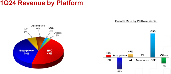
"Moving on to revenue contribution by platform. HPC increased 3% quarter-over-quarter to account for 46% of our first quarter revenue," said Huang. "Smartphone decreased 16% to account for 38%. IoT increased 5% to account for 6%. Automotive remained flat and accounted for 6%, and DCE increased 33% to account for 2%."
Meanwhile, as demand for AI and HPC processors will continue to increase in the coming years, TSMC expects its HPC platform to keep increasing its share in its revenue going forward.
"We expect several AI processors to be the strongest driver of our HPC platform growth and the largest contributor in terms of our overall incremental revenue growth in the next several years," said C.C. Wei, chief executive of TSMC.
AMD has recently expanded its Ryzen 8000 series by introducing the Ryzen 7 8700F and Ryzen 5 8400F processors. Initially launched in China, these chips were added to AMD's global website, signaling they are available worldwide, apparently from April 1st. Built from the recent Zen 4-based Phoenix APUs using the TSMC 4nm node as their Zen 4 mobile chips, these new CPUs lack integrated graphics. However, the Ryzen 7 8700F does include the integrated Ryzen AI NPU for added capabilities in a world currently dominated by AI and moving it directly into the PC.
The company's decision to announce these chips in China aligns with its strategy to offer Ryzen solutions at every price point in the market. Although AMD didn't initially disclose the full specifications of these F-series models, and we did reach out to the company to ask about them, they refused to discuss them with us. Their listing on the website has now been updated with a complete list of specifications and features, with everything but the price mentioned.
| AMD Ryzen 8000G vs. Ryzen 8000F Series (Desktop) Zen 4 (Phoenix) |
|||||||||
| AnandTech | Cores/Threads | Base Freq |
Turbo Freq |
GPU | GPU Freq |
Ryzen AI (NPU) |
L3 Cache (MB) |
TDP | MSRP |
| Ryzen 7 | |||||||||
| Ryzen 7 8700G | 8/16 | 4200 | 5100 | R780M 12 CUs |
2900 | Y | 16 | 65W | $329 |
| Ryzen 7 8700F | 8/16 | 4100 | 5000 | - | - | Y | 16 | 65W | ? |
| Ryzen 5 | |||||||||
| Ryzen 5 8600G | 6/12 | 4300 | 5000 | R760M 8 CUs |
2800 | Y | 16 | 65W | $229 |
| Ryzen 5 8400F | 6/12 | 4200 | 4700 | - | - | N | 16 | 65W | ? |
The Ryzen 7 8700F features an 8C/16T design, with 16MB of L3 cache and the same 65W TDP as the Ryzen 7 8700G. Although the base clock speed is 4.1 GHz, it boosts to 5.0 GHz; this is 100 MHz less on both base/boost clocks than the 8700G. Meanwhile, the Ryzen 5 8400F is a slightly scaled-down version of the Ryzen 8600G APU, with 6C/12, 16MB of L3 cache, and again has a 100 MHz reduction to base clocks compared to the 8600G. Unlike the Ryzen 5 8400F, the Ryzen 7 8700F keeps AMD's Ryzen AI NPU, adding additional capability for generative AI.
The Ryzen 5 8400F can boost up to 4.7 GHz, 300 MHz slower than the Ryzen 5 8600G. AMD also allows overclocking for these new F-series chips, which means users could potentially boost the performance of these processors to match their G-series equivalents.
Pricing details are still pending, but to remain competitive, AMD will likely need to price these CPUs below the 8700G and 8600G, as well as the Ryzen 7 7700 and Ryzen 5 7600. These CPUs offer, albeit very limited, integrated graphics and have double the L3 cache capacity, along with higher boost clocks than the 8000F series chips, so pricing is something to consider whenever pricing becomes available.
CPUs
Optical connectivity – and especially silicon photonics – is expected to become a crucial technology to enable connectivity for next-generation datacenters, particularly those designed HPC applications. With ever-increasing bandwidth requirements needed to keep up with (and keep scaling out) system performance, copper signaling alone won't be enough to keep up. To that end, several companies are developing silicon photonics solutions, including fab providers like TSMC, who this week outlined its 3D Optical Engine roadmap as part of its 2024 North American Technology Symposium, laying out its plan to bring up to 12.8 Tbps optical connectivity to TSMC-fabbed processors.
TSMC's Compact Universal Photonic Engine (COUPE) stacks an electronics integrated circuit on photonic integrated circuit (EIC-on-PIC) using the company's SoIC-X packaging technology. The foundry says that usage of its SoIC-X enables the lowest impedance at the die-to-die interface and therefore the highest energy efficiency. The EIC itself is produced at a 65nm-class process technology.
TSMC's 1st Generation 3D Optical Engine (or COUPE) will be integrated into an OSFP pluggable device running at 1.6 Tbps. That's a transfer rate well ahead of current copper Ethernet standards – which top out at 800 Gbps – underscoring the immediate bandwidth advantage of optical interconnects for heavily-networked compute clusters, never mind the expected power savings.
Looking further ahead, the 2nd Generation of COUPE is designed to integrate into CoWoS packaging as co-packaged optics with a switch, allowing optical interconnections to be brought to the motherboard level. This version COUPE will support data transfer rates of up to 6.40 Tbps with reduced latency compared to the first version.
TSMC's third iteration of COUPE – COUPE running on a CoWoS interposer – is projected to improve on things one step further, increasing transfer rates to 12.8 Tbps while bringing optical connectivity even closer to the processor itself. At present, COUPE-on-CoWoS is in the pathfinding stage of development and TSMC does not have a target date set.
Ultimately, unlike many of its industry peers, TSMC has not participated in the silicon photonics market up until now, leaving this to players like GlobalFoundries. But with its 3D Optical Engine Strategy, the company will enter this important market as it looks to make up for lost time.
Standard CPU coolers, while adequate for managing basic thermal loads, often fall short in terms of noise reduction and superior cooling efficiency. This limitation drives advanced users and system builders to seek aftermarket solutions tailored to their specific needs. The high-end aftermarket cooler market is highly competitive, with manufacturers striving to offer products with exceptional performance.
Endorfy, previously known as SilentiumPC, is a Polish manufacturer that has undergone a significant transformation to expand its presence in global markets. The brand is known for delivering high-performance cooling solutions with a strong focus on balancing efficiency and affordability. By rebranding as Endorfy, the company aims to enter premium market segments while continuing to offer reliable, high-quality cooling products.
SilentiumPC became very popular in the value/mainstream segments of the PC market with their products, the spearhead of which probably was the Fera 5 cooler that we reviewed a little over two years ago and had a remarkable value for money. Today’s review places Endorfy’s largest CPU cooler, the Fortis 5 Dual Fan, on our laboratory test bench. The Fortis 5 is the largest CPU air cooler the company currently offers and is significantly more expensive than the Fera 5, yet it still is a single-tower cooler that strives to strike a balance between value, compatibility, and performance.
Cases/Cooling/PSUs![Micron: U.S. Fabs Will Start Operating in 2026 - 2029 <p align="center"><a href="https://www.anandtech.com/show/21459/micron-u-s-fabs-will-start-operating-in-2026-2029"><img src="https://images.anandtech.com/doci/21459/micron-server-datacenter-general-generic-678_575px.jpg" alt="" /></a></p><p><p>When Micron announced plans to build two new fabs in the U.S. in 2022, the company vaguely said both would come online by the decade's end. Then, in 2023, it began to optimize its spending, which pushed production at these fabrication facilities. This week, the company outlined more precise timeframes for when its fabs in <a href="https://www.anandtech.com/show/17573/micron-breaks-ground-on-its-15-billion-euv-dram-fab-in-the-us">Idaho</a> and <a href="https://www.anandtech.com/show/17606/micron-announces-100-billion-us-fab-complex-a-20year-plan">New York</a> will start operations: this will happen from calendar 2026 to calendar 2029.</p>
<p>"<em>These fab construction investments are necessary to support supply growth for the latter half of this decade,</em>" a statement by Micron in its Q3 FY2024 financial results report <a href="https://investors.micron.com/static-files/a531c7f0-fca2-48f3-8f24-79c945aaa2d2">reads</a>. "<em>This Idaho fab will not contribute to meaningful bit supply until fiscal 2027 and the New York construction capex is not expected to contribute to bit supply growth until fiscal 2028 or later. The timing of future [wafer fab equipment] spend in these fabs will be managed to align supply growth with expected demand growth.</em>"</p>
<p>Micron's fiscal year 2027 starts in September 2026, so the new fab near Boise, Idaho, is set to start operations between September 2026 and September 2027. The company's fiscal 2028 starts in September 2027, so the fab will likely begin operations in calendar 2028 or later, probably depending on the demand for DRAM memory in the coming years. That said, Micron's U.S. memory fabs will begin operations between late 2026 and 2029, which aligns with the company's original plans. </p>
<p>Construction of the fab in Idaho is well underway. In contrast, construction of the New York facility has yet to begin as the company is working on regulatory and permitting processes in the state. </p>
<p>Micron's capital expenditure (CaPex) plan for FY2024 is approximately $8.0 billion, with a decrease in year-over-year spending on wafer fabrication equipment (WFE). In Q4 FY2024, the company will spend around $3 billion on fab construction, new wafer fab tools, and various expansions/upgrades.</p>
<p>Looking ahead to FY2025, the company plans a substantial increase in capex, targeting a mid-30s percentage of revenue to support various technological and facility advancements. In particular, it expects its quarterly CapEx to average above the $3 billion level seen in the fourth quarter of FY2024, which means that it plans to spend about $12 billion in its fiscal 2025, which begins in late September.</p>
<p>Half or more of the total CapEx increase in FY2025 (i.e., over $2 billion) will be allocated to constructing new fabs in Idaho and New York. Meanwhile, the FY2025 CapEx will significantly rise to fund high-bandwidth memory (HBM) assembly and testing and the construction of fabrication and back-end facilities. This increase also includes investments in technology transitions to meet growing demand. </p>
<p>"<em>Fab construction in Idaho is underway, and we are working diligently to complete the regulatory and permitting processes in New York,</em>" said Sanjay Mehrotra, chief executive officer of Micron, at the company's conference call with investors and financial analysts (via <a href="https://seekingalpha.com/article/4701253-micron-technology-inc-mu-q3-2024-earnings-call-transcript?source=content_type%3Areact%7Csection%3ATranscripts%7Csection_asset%3ATranscripts%7Cfirst_level_url%3Asymbol%7Cbutton%3ATitle%7Clock_status%3ANo%7Cline%3A1">SeekingAlpha</a>). "<em>This additional leading-edge greenfield capacity, along with continued technology transition investments in our Asia facilities, is required to meet long-term demand in the second half of this decade and beyond. These investments support our objective to maintain our current bit share over time and to grow our memory bit supply in line with long-term industry bit demand.</em>"</p>
</p> Memory](https://lh3.googleusercontent.com/blogger_img_proxy/AEn0k_th3yEUxB-ObuS9C5SzXCpw5WzJ8D9Myq3B645LPY9iOiDVDNbOuBOhDTkvFhGMOAAMlSWIP5mOp5YDuNxMDXqqXSeuluTi3advY74w1Y7FH7woQrMzXrtydgxG54swDpEJvBUwzfG_94QIdC65TlkjncFKHCdTIfWus7VeFyjFqNM=w72-h72-p-k-no-nu)

When Micron announced plans to build two new fabs in the U.S. in 2022, the company vaguely said both would come online by the decade's end. Then, in 2023, it began to optimize its spending, which pushed production at these fabrication facilities. This week, the company outlined more precise timeframes for when its fabs in Idaho and New York will start operations: this will happen from calendar 2026 to calendar 2029.
"These fab construction investments are necessary to support supply growth for the latter half of this decade," a statement by Micron in its Q3 FY2024 financial results report reads. "This Idaho fab will not contribute to meaningful bit supply until fiscal 2027 and the New York construction capex is not expected to contribute to bit supply growth until fiscal 2028 or later. The timing of future [wafer fab equipment] spend in these fabs will be managed to align supply growth with expected demand growth."
Micron's fiscal year 2027 starts in September 2026, so the new fab near Boise, Idaho, is set to start operations between September 2026 and September 2027. The company's fiscal 2028 starts in September 2027, so the fab will likely begin operations in calendar 2028 or later, probably depending on the demand for DRAM memory in the coming years. That said, Micron's U.S. memory fabs will begin operations between late 2026 and 2029, which aligns with the company's original plans.
Construction of the fab in Idaho is well underway. In contrast, construction of the New York facility has yet to begin as the company is working on regulatory and permitting processes in the state.
Micron's capital expenditure (CaPex) plan for FY2024 is approximately $8.0 billion, with a decrease in year-over-year spending on wafer fabrication equipment (WFE). In Q4 FY2024, the company will spend around $3 billion on fab construction, new wafer fab tools, and various expansions/upgrades.
Looking ahead to FY2025, the company plans a substantial increase in capex, targeting a mid-30s percentage of revenue to support various technological and facility advancements. In particular, it expects its quarterly CapEx to average above the $3 billion level seen in the fourth quarter of FY2024, which means that it plans to spend about $12 billion in its fiscal 2025, which begins in late September.
Half or more of the total CapEx increase in FY2025 (i.e., over $2 billion) will be allocated to constructing new fabs in Idaho and New York. Meanwhile, the FY2025 CapEx will significantly rise to fund high-bandwidth memory (HBM) assembly and testing and the construction of fabrication and back-end facilities. This increase also includes investments in technology transitions to meet growing demand.
"Fab construction in Idaho is underway, and we are working diligently to complete the regulatory and permitting processes in New York," said Sanjay Mehrotra, chief executive officer of Micron, at the company's conference call with investors and financial analysts (via SeekingAlpha). "This additional leading-edge greenfield capacity, along with continued technology transition investments in our Asia facilities, is required to meet long-term demand in the second half of this decade and beyond. These investments support our objective to maintain our current bit share over time and to grow our memory bit supply in line with long-term industry bit demand."
Memory
Standard CPU coolers, while adequate for managing basic thermal loads, often fall short in terms of noise reduction and superior cooling efficiency. This limitation drives advanced users and system builders to seek aftermarket solutions tailored to their specific needs. The high-end aftermarket cooler market is highly competitive, with manufacturers striving to offer products with exceptional performance.
Endorfy, previously known as SilentiumPC, is a Polish manufacturer that has undergone a significant transformation to expand its presence in global markets. The brand is known for delivering high-performance cooling solutions with a strong focus on balancing efficiency and affordability. By rebranding as Endorfy, the company aims to enter premium market segments while continuing to offer reliable, high-quality cooling products.
SilentiumPC became very popular in the value/mainstream segments of the PC market with their products, the spearhead of which probably was the Fera 5 cooler that we reviewed a little over two years ago and had a remarkable value for money. Today’s review places Endorfy’s largest CPU cooler, the Fortis 5 Dual Fan, on our laboratory test bench. The Fortis 5 is the largest CPU air cooler the company currently offers and is significantly more expensive than the Fera 5, yet it still is a single-tower cooler that strives to strike a balance between value, compatibility, and performance.
Cases/Cooling/PSUs
When Micron announced plans to build two new fabs in the U.S. in 2022, the company vaguely said both would come online by the decade's end. Then, in 2023, it began to optimize its spending, which pushed production at these fabrication facilities. This week, the company outlined more precise timeframes for when its fabs in Idaho and New York will start operations: this will happen from calendar 2026 to calendar 2029.
"These fab construction investments are necessary to support supply growth for the latter half of this decade," a statement by Micron in its Q3 FY2024 financial results report reads. "This Idaho fab will not contribute to meaningful bit supply until fiscal 2027 and the New York construction capex is not expected to contribute to bit supply growth until fiscal 2028 or later. The timing of future [wafer fab equipment] spend in these fabs will be managed to align supply growth with expected demand growth."
Micron's fiscal year 2027 starts in September 2026, so the new fab near Boise, Idaho, is set to start operations between September 2026 and September 2027. The company's fiscal 2028 starts in September 2027, so the fab will likely begin operations in calendar 2028 or later, probably depending on the demand for DRAM memory in the coming years. That said, Micron's U.S. memory fabs will begin operations between late 2026 and 2029, which aligns with the company's original plans.
Construction of the fab in Idaho is well underway. In contrast, construction of the New York facility has yet to begin as the company is working on regulatory and permitting processes in the state.
Micron's capital expenditure (CaPex) plan for FY2024 is approximately $8.0 billion, with a decrease in year-over-year spending on wafer fabrication equipment (WFE). In Q4 FY2024, the company will spend around $3 billion on fab construction, new wafer fab tools, and various expansions/upgrades.
Looking ahead to FY2025, the company plans a substantial increase in capex, targeting a mid-30s percentage of revenue to support various technological and facility advancements. In particular, it expects its quarterly CapEx to average above the $3 billion level seen in the fourth quarter of FY2024, which means that it plans to spend about $12 billion in its fiscal 2025, which begins in late September.
Half or more of the total CapEx increase in FY2025 (i.e., over $2 billion) will be allocated to constructing new fabs in Idaho and New York. Meanwhile, the FY2025 CapEx will significantly rise to fund high-bandwidth memory (HBM) assembly and testing and the construction of fabrication and back-end facilities. This increase also includes investments in technology transitions to meet growing demand.
"Fab construction in Idaho is underway, and we are working diligently to complete the regulatory and permitting processes in New York," said Sanjay Mehrotra, chief executive officer of Micron, at the company's conference call with investors and financial analysts (via SeekingAlpha). "This additional leading-edge greenfield capacity, along with continued technology transition investments in our Asia facilities, is required to meet long-term demand in the second half of this decade and beyond. These investments support our objective to maintain our current bit share over time and to grow our memory bit supply in line with long-term industry bit demand."
Memory

Kioxia's booth at FMS 2024 was a busy one with multiple technology demonstrations keeping visitors occupied. A walk-through of the BiCS 8 manufacturing process was the first to grab my attention. Kioxia and Western Digital announced the sampling of BiCS 8 in March 2023. We had touched briefly upon its CMOS Bonded Array (CBA) scheme in our coverage of Kioxial's 2Tb QLC NAND device and coverage of Western Digital's 128 TB QLC enterprise SSD proof-of-concept demonstration. At Kioxia's booth, we got more insights.

Traditionally, fabrication of flash chips involved placement of the associate logic circuitry (CMOS process) around the periphery of the flash array. The process then moved on to putting the CMOS under the cell array, but the wafer development process was serialized with the CMOS logic getting fabricated first followed by the cell array on top. However, this has some challenges because the cell array requires a high-temperature processing step to ensure higher reliability that can be detrimental to the health of the CMOS logic. Thanks to recent advancements in wafer bonding techniques, the new CBA process allows the CMOS wafer and cell array wafer to be processed independently in parallel and then pieced together, as shown in the models above.

The BiCS 8 3D NAND incorporates 218 layers, compared to 112 layers in BiCS 5 and 162 layers in BiCS 6. The company decided to skip over BiCS 7 (or, rather, it was probably a short-lived generation meant as an internal test vehicle). The generation retains the four-plane charge trap structure of BiCS 6. In its TLC avatar, it is available as a 1 Tbit device. The QLC version is available in two capacities - 1 Tbit and 2 Tbit.
Kioxia also noted that while the number of layers (218) doesn't compare favorably with the latest layer counts from the competition, its lateral scaling / cell shrinkage has enabled it to be competitive in terms of bit density as well as operating speeds (3200 MT/s). For reference, the latest shipping NAND from Micron - the G9 - has 276 layers with a bit density in TLC mode of 21 Gbit/mm2, and operates at up to 3600 MT/s. However, its 232L NAND operates only up to 2400 MT/s and has a bit density of 14.6 Gbit/mm2.
It must be noted that the CBA hybrid bonding process has advantages over the current processes used by other vendors - including Micron's CMOS under array (CuA) and SK hynix's 4D PUC (periphery-under-chip) developed in the late 2010s. It is expected that other NAND vendors will also move eventually to some variant of the hybrid bonding scheme used by Kioxia.
Storage
It is with great sadness that I find myself penning the hardest news post I’ve ever needed to write here at AnandTech. After over 27 years of covering the wide – and wild – world of computing hardware, today is AnandTech’s final day of publication.
For better or worse, we’ve reached the end of a long journey – one that started with a review of an AMD processor, and has ended with the review of an AMD processor. It’s fittingly poetic, but it is also a testament to the fact that we’ve spent the last 27 years doing what we love, covering the chips that are the lifeblood of the computing industry.
A lot of things have changed in the last quarter-century – in 1997 NVIDIA had yet to even coin the term “GPU” – and we’ve been fortunate to watch the world of hardware continue to evolve over the time period. We’ve gone from boxy desktop computers and laptops that today we’d charitably classify as portable desktops, to pocket computers where even the cheapest budget device puts the fastest PC of 1997 to shame.
The years have also brought some monumental changes to the world of publishing. AnandTech was hardly the first hardware enthusiast website, nor will we be the last. But we were fortunate to thrive in the past couple of decades, when so many of our peers did not, thanks to a combination of hard work, strategic investments in people and products, even more hard work, and the support of our many friends, colleagues, and readers.
Still, few things last forever, and the market for written tech journalism is not what it once was – nor will it ever be again. So, the time has come for AnandTech to wrap up its work, and let the next generation of tech journalists take their place within the zeitgeist.
It has been my immense privilege to write for AnandTech for the past 19 years – and to manage it as its editor-in-chief for the past decade. And while I carry more than a bit of remorse in being AnandTech’s final boss, I can at least take pride in everything we’ve accomplished over the years, whether it’s lauding some legendary products, writing technology primers that still remain relevant today, or watching new stars rise in expected places. There is still more that I had wanted AnandTech to do, but after 21,500 articles, this was a good start.
And while the AnandTech staff is riding off into the sunset, I am happy to report that the site itself won’t be going anywhere for a while. Our publisher, Future PLC, will be keeping the AnandTech website and its many articles live indefinitely. So that all of the content we’ve created over the years remains accessible and citable. Even without new articles to add to the collection, I expect that many of the things we’ve written over the past couple of decades will remain relevant for years to come – and remain accessible just as long.
The AnandTech Forums will also continue to be operated by Future’s community team and our dedicated troop of moderators. With forum threads going back to 1999 (and some active members just as long), the forums have a history almost as long and as storied as AnandTech itself (wounded monitor children, anyone?). So even when AnandTech is no longer publishing articles, we’ll still have a place for everyone to talk about the latest in technology – and have those discussions last longer than 48 hours.
Finally, for everyone who still needs their technical writing fix, our formidable opposition of the last 27 years and fellow Future brand, Tom’s Hardware, is continuing to cover the world of technology. There are a couple of familiar AnandTech faces already over there providing their accumulated expertise, and the site will continue doing its best to provide a written take on technology news.
As I look back on everything AnandTech has accomplished over the past 27 years, there are more than a few people, groups, and companies that I would like to thank on behalf of both myself and AnandTech as a whole.
First and foremost, I cannot thank enough all the editors who have worked for AnandTech over the years. T... Site Updates


G.Skill on Tuesday introduced its ultra-low-latency DDR5-6400 memory modules that feature a CAS latency of 30 clocks, which appears to be the industry's most aggressive timings yet for DDR5-6400 sticks. The modules will be available for both AMD and Intel CPU-based systems.
With every new generation of DDR memory comes an increase in data transfer rates and an extension of relative latencies. While for the vast majority of applications, the increased bandwidth offsets the performance impact of higher timings, there are applications that favor low latencies. However, shrinking latencies is sometimes harder than increasing data transfer rates, which is why low-latency modules are rare.
Nonetheless, G.Skill has apparently managed to cherry-pick enough DDR5 memory chips and build appropriate printed circuit boards to produce DDR5-6400 modules with CL30 timings, which are substantially lower than the CL46 timings recommended by JEDEC for this speed bin. This means that while JEDEC-standard modules have an absolute latency of 14.375 ns, G.Skill's modules can boast a latency of just 9.375 ns – an approximately 35% decrease.
G.Skill's DDR5-6400 CL30 39-39-102 modules have a capacity of 16 GB and will be available in 32 GB dual-channel kits, though the company does not disclose voltages, which are likely considerably higher than those standardized by JEDEC.
The company plans to make its DDR5-6400 modules available both for AMD systems with EXPO profiles (Trident Z5 Neo RGB and Trident Z5 Royal Neo) and for Intel-powered PCs with XMP 3.0 profiles (Trident Z5 RGB and Trident Z5 Royal). For AMD AM5 systems that have a practical limitation of 6000 MT/s – 6400 MT/s for DDR5 memory (as this is roughly as fast as AMD's Infinity Fabric can operate at with a 1:1 ratio), the new modules will be particularly beneficial for AMD's Ryzen 7000 and Ryzen 9000-series processors.
G.Skill notes that since its modules are non-standard, they will not work with all systems but will operate on high-end motherboards with properly cooled CPUs.
The new ultra-low-latency memory kits will be available worldwide from G.Skill's partners starting in late August 2024. The company did not disclose the pricing of these modules, but since we are talking about premium products that boast unique specifications, they are likely to be priced accordingly.
Memory
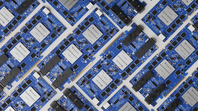
Tenstorrent has unveiled its next-generation Wormhole processor for AI workloads that promises to offer decent performance at a low price. The company currently offers two add-on PCIe cards carrying one or two Wormhole processors as well as TT-LoudBox, and TT-QuietBox workstations aimed at software developers. The whole of today's release is aimed at developers rather than those who will deploy the Wormhole boards for their commercial workloads.
“It is always rewarding to get more of our products into developer hands. Releasing development systems with our Wormhole™ card helps developers scale up and work on multi-chip AI software.” said Jim Keller, CEO of Tenstorrent. “In addition to this launch, we are excited that the tape-out and power-on for our second generation, Blackhole, is going very well.”
Each Wormhole processor packs 72 Tensix cores (featuring five RISC-V cores supporting various data formats) with 108 MB of SRAM to deliver 262 FP8 TFLOPS at 1 GHz at 160W thermal design power. A single-chip Wormhole n150 card carries 12 GB of GDDR6 memory featuring a 288 GB/s bandwidth.
Wormhole processors offer flexible scalability to meet the varying needs of workloads. In a standard workstation setup with four Wormhole n300 cards, the processors can merge to function as a single unit, appearing as a unified, extensive network of Tensix cores to the software. This configuration allows the accelerators to either work on the same workload, be divided among four developers or run up to eight distinct AI models simultaneously. A crucial feature of this scalability is that it operates natively without the need for virtualization. In data center environments, Wormhole processors will scale both inside one machine using PCIe or outside of a single machine using Ethernet.
From performance standpoint, Tenstorrent's single-chip Wormhole n150 card (72 Tensix cores at 1 GHz, 108 MB SRAM, 12 GB GDDR6 at 288 GB/s) is capable of 262 FP8 TFLOPS at 160W, whereas the dual-chip Wormhole n300 board (128 Tensix cores at 1 GHz, 192 MB SRAM, aggregated 24 GB GDDR6 at 576 GB/s) can offer up to 466 FP8 TFLOPS at 300W (according to Tom's Hardware).
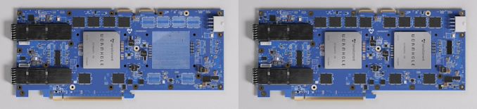
To put that 466 FP8 TFLOPS at 300W number into context, let's compare it to what AI market leader Nvidia has to offer at this thermal design power. Nvidia's A100 does not support FP8, but it does support INT8 and its peak performance is 624 TOPS (1,248 TOPS with sparsity). By contrast, Nvidia's H100 supports FP8 and its peak performance is massive 1,670 TFLOPS (3,341 TFLOPS with sparsity) at 300W, which is a big difference from Tenstorrent's Wormhole n300.
There is a big catch though. Tenstorrent's Wormhole n150 is offered for $999, whereas n300 is available for $1,399. By contrast, one Nvidia H100 card can retail for $30,000, depending on quantities. Of course, we do not know whether four or eight Wormhole processors can indeed deliver the performance of a single H300, though they will do so at 600W or 1200W TDP, respectively.
In addition to cards, Tenstorrent offers developers pre-built workstations with four n300 cards inside the less expensive Xeon-based TT-LoudBox with active cooling and a premium EPYC-powered TT-QuietBox with liquid cooling.
Sources: Tenstorrent, Tom's Hardware
AI
Kioxia's booth at FMS 2024 was a busy one with multiple technology demonstrations keeping visitors occupied. A walk-through of the BiCS 8 manufacturing process was the first to grab my attention. Kioxia and Western Digital announced the sampling of BiCS 8 in March 2023. We had touched briefly upon its CMOS Bonded Array (CBA) scheme in our coverage of Kioxial's 2Tb QLC NAND device and coverage of Western Digital's 128 TB QLC enterprise SSD proof-of-concept demonstration. At Kioxia's booth, we got more insights.
Traditionally, fabrication of flash chips involved placement of the associate logic circuitry (CMOS process) around the periphery of the flash array. The process then moved on to putting the CMOS under the cell array, but the wafer development process was serialized with the CMOS logic getting fabricated first followed by the cell array on top. However, this has some challenges because the cell array requires a high-temperature processing step to ensure higher reliability that can be detrimental to the health of the CMOS logic. Thanks to recent advancements in wafer bonding techniques, the new CBA process allows the CMOS wafer and cell array wafer to be processed independently in parallel and then pieced together, as shown in the models above.
The BiCS 8 3D NAND incorporates 218 layers, compared to 112 layers in BiCS 5 and 162 layers in BiCS 6. The company decided to skip over BiCS 7 (or, rather, it was probably a short-lived generation meant as an internal test vehicle). The generation retains the four-plane charge trap structure of BiCS 6. In its TLC avatar, it is available as a 1 Tbit device. The QLC version is available in two capacities - 1 Tbit and 2 Tbit.
Kioxia also noted that while the number of layers (218) doesn't compare favorably with the latest layer counts from the competition, its lateral scaling / cell shrinkage has enabled it to be competitive in terms of bit density as well as operating speeds (3200 MT/s). For reference, the latest shipping NAND from Micron - the G9 - has 276 layers with a bit density in TLC mode of 21 Gbit/mm2, and operates at up to 3600 MT/s. However, its 232L NAND operates only up to 2400 MT/s and has a bit density of 14.6 Gbit/mm2.
It must be noted that the CBA hybrid bonding process has advantages over the current processes used by other vendors - including Micron's CMOS under array (CuA) and SK hynix's 4D PUC (periphery-under-chip) developed in the late 2010s. It is expected that other NAND vendors will also move eventually to some variant of the hybrid bonding scheme used by Kioxia.
Storage
Lorem Ipsum is simply dummy text of the printing and typesetting industry. Lorem Ipsum has been the industry's.
Standard CPU coolers, while adequate for managing basic thermal loads, often fall short in terms of noise reduction and superior cooling efficiency. This limitation drives advanced users and system builders to seek aftermarket solutions tailored to their specific needs. The high-end aftermarket cooler market is highly competitive, with manufacturers striving to offer products with exceptional performance.
Endorfy, previously known as SilentiumPC, is a Polish manufacturer that has undergone a significant transformation to expand its presence in global markets. The brand is known for delivering high-performance cooling solutions with a strong focus on balancing efficiency and affordability. By rebranding as Endorfy, the company aims to enter premium market segments while continuing to offer reliable, high-quality cooling products.
SilentiumPC became very popular in the value/mainstream segments of the PC market with their products, the spearhead of which probably was the Fera 5 cooler that we reviewed a little over two years ago and had a remarkable value for money. Today’s review places Endorfy’s largest CPU cooler, the Fortis 5 Dual Fan, on our laboratory test bench. The Fortis 5 is the largest CPU air cooler the company currently offers and is significantly more expensive than the Fera 5, yet it still is a single-tower cooler that strives to strike a balance between value, compatibility, and performance.
Cases/Cooling/PSUs
When Micron announced plans to build two new fabs in the U.S. in 2022, the company vaguely said both would come online by the decade's end. Then, in 2023, it began to optimize its spending, which pushed production at these fabrication facilities. This week, the company outlined more precise timeframes for when its fabs in Idaho and New York will start operations: this will happen from calendar 2026 to calendar 2029.
"These fab construction investments are necessary to support supply growth for the latter half of this decade," a statement by Micron in its Q3 FY2024 financial results report reads. "This Idaho fab will not contribute to meaningful bit supply until fiscal 2027 and the New York construction capex is not expected to contribute to bit supply growth until fiscal 2028 or later. The timing of future [wafer fab equipment] spend in these fabs will be managed to align supply growth with expected demand growth."
Micron's fiscal year 2027 starts in September 2026, so the new fab near Boise, Idaho, is set to start operations between September 2026 and September 2027. The company's fiscal 2028 starts in September 2027, so the fab will likely begin operations in calendar 2028 or later, probably depending on the demand for DRAM memory in the coming years. That said, Micron's U.S. memory fabs will begin operations between late 2026 and 2029, which aligns with the company's original plans.
Construction of the fab in Idaho is well underway. In contrast, construction of the New York facility has yet to begin as the company is working on regulatory and permitting processes in the state.
Micron's capital expenditure (CaPex) plan for FY2024 is approximately $8.0 billion, with a decrease in year-over-year spending on wafer fabrication equipment (WFE). In Q4 FY2024, the company will spend around $3 billion on fab construction, new wafer fab tools, and various expansions/upgrades.
Looking ahead to FY2025, the company plans a substantial increase in capex, targeting a mid-30s percentage of revenue to support various technological and facility advancements. In particular, it expects its quarterly CapEx to average above the $3 billion level seen in the fourth quarter of FY2024, which means that it plans to spend about $12 billion in its fiscal 2025, which begins in late September.
Half or more of the total CapEx increase in FY2025 (i.e., over $2 billion) will be allocated to constructing new fabs in Idaho and New York. Meanwhile, the FY2025 CapEx will significantly rise to fund high-bandwidth memory (HBM) assembly and testing and the construction of fabrication and back-end facilities. This increase also includes investments in technology transitions to meet growing demand.
"Fab construction in Idaho is underway, and we are working diligently to complete the regulatory and permitting processes in New York," said Sanjay Mehrotra, chief executive officer of Micron, at the company's conference call with investors and financial analysts (via SeekingAlpha). "This additional leading-edge greenfield capacity, along with continued technology transition investments in our Asia facilities, is required to meet long-term demand in the second half of this decade and beyond. These investments support our objective to maintain our current bit share over time and to grow our memory bit supply in line with long-term industry bit demand."
Memory
Social Plugin