


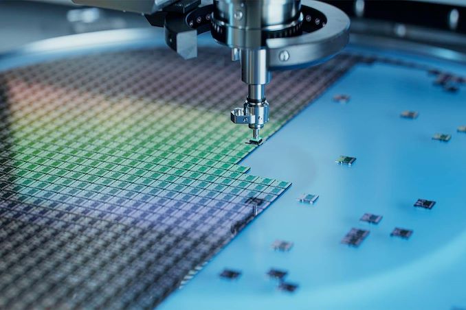
![Rapidus Wants to Offer Fully Automated Packaging for 2nm Fab to Cut Chip Lead Times <p align="center"><a href="https://www.anandtech.com/show/21525/rapidus-2nm-fully-automated-chip-packaging-to-cut-lead-times"><img src="https://images.anandtech.com/doci/21525/intel-foundry-wafer-semiconductor-fab-ifs-678_575px.jpg" alt="" /></a></p><p><p>One of the core challenges that Rapidus will face when it kicks off volume production of chips on its 2nm-class process technology in 2027 is lining up customers. With Intel, Samsung, and TSMC all slated to offer their own 2nm-class nodes by that time, Rapidus will need some kind of advantage to attract customers away from its more established rivals. To that end, the company thinks they've found their edge: fully automated packaging that will allow for shorter chip lead times than manned packaging operations.</p>
<p>In an interview with <a href="https://asia.nikkei.com/Editor-s-Picks/Interview/Japan-s-Rapidus-to-fully-automate-2-nm-chip-fab-president-says">Nikkei</a>, Rapidus' president, Atsuyoshi Koike, outlined the company's vision to use advanced packaging as a competitive edge for the new fab. <a href="https://www.anandtech.com/show/21411/rapidus-adds-chip-packaging-services-to-plans-for-32b-2nm-fab">The Hokkaido facility</a>, which is currently under construction and is expecting to begin equipment installation this December, is already slated to both produce chips and offer advanced packaging services within the same facility, an industry first. But ultimately, Rapidus biggest plan to differentiate itself is by automating the back-end fab processes (chip packaging) to provide significantly faster turnaround times.</p>
<p>Rapidus is targetting back-end production in particular as, compared to front-end (lithography) production, back-end production still heavily relies on human labor. No other advanced packaging fab has fully automated the process thus far, which provides for a degree of flexibility, but slows throughput. But with automation in place to handle this aspect of chip production, Rapidus would be able to increase chip packaging efficiency and speed, which is crucial as chip assembly tasks become more complex. Rapidus is also collaborating with multiple Japanese suppliers to source materials for back-end production. </p>
<p>"In the past, Japanese chipmakers tried to keep their technology development exclusively in-house, which pushed up development costs and made them less competitive," Koike told Nikkei. "[Rapidus plans to] open up technology that should be standardized, bringing down costs, while handling important technology in-house." </p>
<p>Financially, Rapidus faces a significant challenge, needing a total of ¥5 trillion ($35 billion) by the time mass production starts in 2027. The company estimates that ¥2 trillion will be required by 2025 for prototype production. While the Japanese government has provided ¥920 billion in aid, Rapidus still needs to secure substantial funding from private investors.</p>
<p>Due to its lack of track record and experience of chip production as. well as limited visibility for success, Rapidus is finding it difficult to attract private financing. The company is in discussions with the government to make it easier to raise capital, including potential loan guarantees, and is hopeful that new legislation will assist in this effort.</p>
</p> Semiconductors](https://lh3.googleusercontent.com/blogger_img_proxy/AEn0k_t1_XbM-t6EpYX8N541GGD-P9T0lTZic0T_x-DymshvasuVH1YwKiO6Ooqzc-tX4mN5xrbez0XFQRnpd8x1bp5RfLvyv0z0-t5sMjxJkos4kt39mDnRyeo_Gfv5D7Km9VoI-JntBEx0kJcwJHKYeyiNxYq8mPI1yAZtRiS_CKROpAkN=w72-h72-p-k-no-nu)


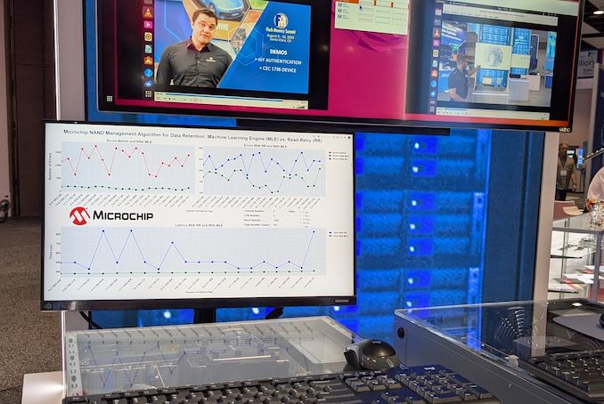
Kioxia Demonstrates Optical Interface SSDs for Data Centers 
A few years back, the Japanese government's New Energy and Industrial Technology Development Organization (NEDO ) allocated funding for the development of green datacenter technologies. With the aim to obtain up to 40% savings in overall power consumption, several Japanese companies have been developing an optical interface for their enterprise SSDs. And at this year's FMS, Kioxia had their optical interface on display.

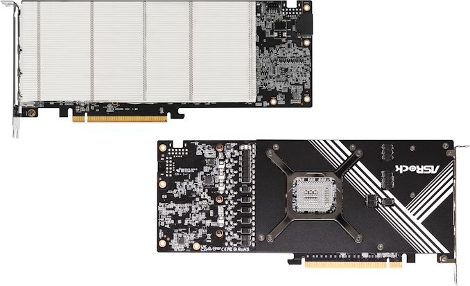
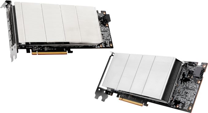
For this demonstration, Kioxia took its existing CM7 enterprise SSD and created an optical interface for it. A PCIe card with on-board optics developed by Kyocera is installed in the server slot. An optical interface allows data transfer over long distances (it was 40m in the demo, but Kioxia promises lengths of up to 100m for the cable in the future). This allows the storage to be kept in a separate room with minimal cooling requirements compared to the rack with the CPUs and GPUs. Disaggregation of different server components will become an option as very high throughput interfaces such as PCIe 7.0 (with 128 GT/s rates) become available.

The demonstration of the optical SSD showed a slight loss in IOPS performance, but a significant advantage in the latency metric over the shipping enterprise SSD behind a copper network link. Obviously, there are advantages in wiring requirements and signal integrity maintenance with optical links.
Being a proof-of-concept demonstration, we do see the requirement for an industry-standard approach if this were to gain adoption among different datacenter vendors. The PCI-SIG optical workgroup will need to get its act together soon to create a standards-based approach to this problem.
Storage


Social Plugin