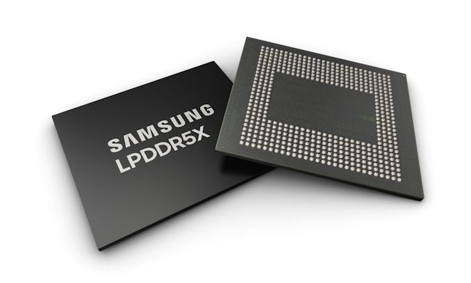
Samsung today has announced that they have developed an even faster generation of LPDDR5X memory that is set to top out at LPDDR5X-10700 speeds. The updated memory is slated to offer 25% better performance and 30% greater capacity compared to existing mobile DRAM devices from the company. The new chips also appear to be tangibly faster than Micron's LPDDR5X memory and SK hynix's LPDDR5T chips.
Samsung's forthcoming LPDDR5X devices feature a data transfer rate of 10.7 GT/s as well as maximum capacity per stack of 32 GB. This allows Samsung's clients to equip their latest smartphones or laptops with 32 GB of low-power memory using just one DRAM package, which greatly simplifies their designs. Samsung says that 32 GB of memory will be particularly beneficial for on-device AI applications.
Samsung is using its latest-generation 12nm-class DRAM process technology to make its LPDDR5X-10700 devices, which allows the company to achieve the smallest LPDDR device size in the industry, the memory maker said.
In terms of power efficiency, Samsung claims that they have integrated multiple new power-saving features into the new LPDDR5X devices. These include an optimized power variation system that adjusts energy consumption based on workload, and expanded intervals for low-power mode that extend the periods of energy saving. These innovations collectively enhance power efficiency by 25% compared to earlier versions, benefiting mobile platforms by extending battery life, the company said.
“As demand for low-power, high-performance memory increases, LPDDR DRAM is expected to expand its applications from mainly mobile to other areas that traditionally require higher performance and reliability such as PCs, accelerators, servers and automobiles,” said YongCheol Bae, Executive Vice President of Memory Product Planning of the Memory Business at Samsung Electronics. “Samsung will continue to innovate and deliver optimized products for the upcoming on-device AI era through close collaboration with customers.”
Samsung plans to initiate mass production of the 10.7 GT/s LPDDR5X DRAM in the second half of this year. This follows a series of compatibility tests with mobile application processors and device manufacturers to ensure seamless integration into future products.
DRAMSK Hynix and TSMC Team Up for HBM4 Development SK hynix and TSMC announced early on Friday that they had signed a memorandum of understanding to collaborate on developing the next-generation HBM4 memory and advanced packaging technology. The initiative is designed to speed up the adoption of HBM4 memory and solidify SK hynix's and TSMC's leading positions in high-bandwidth memory and advanced processor applications. The primary focus of SK hynix's and TSMC's initial efforts will be to enhance the performance of the HBM4 stack's base die, which (if we put it very simply) acts like an ultra-wide interface between memory devices and host processors. With HBM4, SK hynix plans to use one of TSMC's advanced logic process technologies to build base dies to pack additional features and I/O pins within the confines of existing spatial constraints. This collaborative approach also enables SK hynix to customize HBM solutions to satisfy diverse customer performance and energy efficiency requirements. SK hynix has been touting custom HBM solutions for a while, and teaming up with TSMC will undoubtedly help with this. "TSMC and SK hynix have already established a strong partnership over the years. We've worked together in integrating the most advanced logic and state-of-the art HBM in providing the world's leading AI solutions," said Dr. Kevin Zhang, Senior Vice President of TSMC's Business Development and Overseas Operations Office, and Deputy Co-Chief Operating Officer. "Looking ahead to the next-generation HBM4, we're confident that we will continue to work closely in delivering the best-integrated solutions to unlock new AI innovations for our common customers." Furthermore, the collaboration extends to optimizing the integration of SK hynix's HBM with TSMC's CoWoS advanced packaging technology. CoWoS is among the most popular specialized 2.5D packaging process technologies for integrating logic chips and stacked HBM into a unified module. For now, it is expected that HBM4 memory will be integrated with logic processors using direct bonding. However, some of TSMC's customers might prefer to use an ultra-advanced version of CoWoS to integrate HBM4 with their processors. "We expect a strong partnership with TSMC to help accelerate our efforts for open collaboration with our customers and develop the industry's best-performing HBM4," said Justin Kim, President and the Head of AI Infra at SK hynix. "With this cooperation in place, we will strengthen our market leadership as the total AI memory provider further by beefing up competitiveness in the space of the custom memory platform." Memory
TSMC's 1.6nm Technology Announced for Late 2026: A16 with "Super Power Rail" Backside Power With the arrival of spring comes showers, flowers, and in the technology industry, TSMC's annual technology symposium series. With customers spread all around the world, the Taiwanese pure play foundry has adopted an interesting strategy for updating its customers on its fab plans, holding a series of symposiums from Silicon Valley to Shanghai. Kicking off the series every year – and giving us our first real look at TSMC's updated foundry plans for the coming years – is the Santa Clara stop, where yesterday the company has detailed several new technologies, ranging from more advanced lithography processes to massive, wafer-scale chip packing options. Today we're publishing several stories based on TSMC's different offerings, starting with TSMC's marquee announcement: their A16 process node. Meanwhile, for the rest of our symposium stories, please be sure to check out the related reading below, and check back for additional stories. TSMC 2nm Update: N2 In 2025, N2P Loses Backside Power, and NanoFlex Brings Optimal Cells TSMC Preps Cheaper 4nm N4C Process For 2025, Aiming For 8.5% Cost Reduction TSMC's System-on-Wafer Platform Goes 3D: CoW-SoW Stacks Up the Chips TSMC Jumps Into Silicon Photonics, Lays Out Roadmap For 12.8 Tbps COUPE On-Package Interconnect Headlining its Silicon Valley stop, TSMC announced its first 'angstrom-class' process technology: A16. Following a production schedule shift that has seen backside power delivery network technology (BSPDN) removed from TSMC's N2P node, the new 1.6nm-class production node will now be the first process to introduce BSPDN to TSMC's chipmaking repertoire. With the addition of backside power capabilities and other improvements, TSMC expects A16 to offer significantly improved performance and energy efficiency compared to TSMC's N2P fabrication process. It will be available to TSMC's clients starting H2 2026.
Standard CPU coolers, while adequate for managing basic thermal loads, often fall short in terms of noise reduction and superior cooling efficiency. This limitation drives advanced users and system builders to seek aftermarket solutions tailored to their specific needs. The high-end aftermarket cooler market is highly competitive, with manufacturers striving to offer products with exceptional performance.
Endorfy, previously known as SilentiumPC, is a Polish manufacturer that has undergone a significant transformation to expand its presence in global markets. The brand is known for delivering high-performance cooling solutions with a strong focus on balancing efficiency and affordability. By rebranding as Endorfy, the company aims to enter premium market segments while continuing to offer reliable, high-quality cooling products.
SilentiumPC became very popular in the value/mainstream segments of the PC market with their products, the spearhead of which probably was the Fera 5 cooler that we reviewed a little over two years ago and had a remarkable value for money. Today’s review places Endorfy’s largest CPU cooler, the Fortis 5 Dual Fan, on our laboratory test bench. The Fortis 5 is the largest CPU air cooler the company currently offers and is significantly more expensive than the Fera 5, yet it still is a single-tower cooler that strives to strike a balance between value, compatibility, and performance.
Cases/Cooling/PSUsUnder the CHIPS & Science Act, the U.S. government provided tens of billions of dollars in grants and loans to the world's leading maker of chips, such as Intel, Samsung, and TSMC, which will significantly expand the country's semiconductor production industry in the coming years. However, most chips are typically tested, assembled, and packaged in Asia, which has left the American supply chain incomplete. Addressing this last gap in the government's domestic chip production plans, these past couple of weeks the U.S. government signed memorandums of understanding worth about $1.5 billion with Amkor and SK hynix to support their efforts to build chip packaging facilities in the U.S.
Amkor plans to build a $2 billion advanced packaging facility near Peoria, Arizona, to test and assemble chips produced by TSMC at its Fab 21 near Phoenix, Arizona. The company signed a MOU that offers $400 million in direct funding and access to $200 million in loans under the CHIPS & Science Act. In addition, the company plans to take advantage of a 25% investment tax credit on eligible capital expenditures.
Set to be strategically positioned near TSMC's upcoming Fab 21 complex in Arizona, Amkor's Peoria facility will occupy 55 acres and, when fully completed, will feature over 500,000 square feet (46,451 square meters) of cleanroom space, more than twice the size of Amkor's advanced packaging site in Vietnam. Although the company has not disclosed the exact capacity or the specific technologies the facility will support, it is expected to cater to a wide range of industries, including automotive, high-performance computing, and mobile technologies. This suggests the new plant will offer diverse packaging solutions, including traditional, 2.5D, and 3D technologies.
Amkor has collaborated extensively with Apple on the vision and initial setup of the Peoria facility, as Apple is slated to be the facility's first and largest customer, marking a significant commitment from the tech giant. This partnership highlights the importance of the new facility in reinforcing the U.S. semiconductor supply chain and positioning Amkor as a key partner for companies relying on TSMC's manufacturing capabilities. The project is expected to generate around 2,000 jobs and is scheduled to begin operations in 2027.
This week SK hynix also signed a preliminary agreement with the U.S. government to receive up to $450 million in direct funding and $500 million in loans to build an advanced memory packaging facility in West Lafayette, Indiana.
The proposed facility is scheduled to begin operations in 2028, which means that it will assemble HBM4 or HBM4E memory. Meanwhile, DRAM devices for high bandwidth memory (HBM) stacks will still be produced in South Korea. Nonetheless, packing finished HBM4/HBM4E in the U.S. and possibly integrating these memory modules with high-end processors is a big deal.
In addition to building its packaging plant, SK hynix plans to collaborate with Purdue University and other local research institutions to advance semiconductor technology and packaging innovations. This partnership is intended to bolster research and development in the region, positioning the facility as a hub for AI technology and skilled employment.
SemiconductorsStandard CPU coolers, while adequate for managing basic thermal loads, often fall short in terms of noise reduction and superior cooling efficiency. This limitation drives advanced users and system builders to seek aftermarket solutions tailored to their specific needs. The high-end aftermarket cooler market is highly competitive, with manufacturers striving to offer products with exceptional performance.
Endorfy, previously known as SilentiumPC, is a Polish manufacturer that has undergone a significant transformation to expand its presence in global markets. The brand is known for delivering high-performance cooling solutions with a strong focus on balancing efficiency and affordability. By rebranding as Endorfy, the company aims to enter premium market segments while continuing to offer reliable, high-quality cooling products.
SilentiumPC became very popular in the value/mainstream segments of the PC market with their products, the spearhead of which probably was the Fera 5 cooler that we reviewed a little over two years ago and had a remarkable value for money. Today’s review places Endorfy’s largest CPU cooler, the Fortis 5 Dual Fan, on our laboratory test bench. The Fortis 5 is the largest CPU air cooler the company currently offers and is significantly more expensive than the Fera 5, yet it still is a single-tower cooler that strives to strike a balance between value, compatibility, and performance.
Cases/Cooling/PSUsUnder the CHIPS & Science Act, the U.S. government provided tens of billions of dollars in grants and loans to the world's leading maker of chips, such as Intel, Samsung, and TSMC, which will significantly expand the country's semiconductor production industry in the coming years. However, most chips are typically tested, assembled, and packaged in Asia, which has left the American supply chain incomplete. Addressing this last gap in the government's domestic chip production plans, these past couple of weeks the U.S. government signed memorandums of understanding worth about $1.5 billion with Amkor and SK hynix to support their efforts to build chip packaging facilities in the U.S.
Amkor plans to build a $2 billion advanced packaging facility near Peoria, Arizona, to test and assemble chips produced by TSMC at its Fab 21 near Phoenix, Arizona. The company signed a MOU that offers $400 million in direct funding and access to $200 million in loans under the CHIPS & Science Act. In addition, the company plans to take advantage of a 25% investment tax credit on eligible capital expenditures.
Set to be strategically positioned near TSMC's upcoming Fab 21 complex in Arizona, Amkor's Peoria facility will occupy 55 acres and, when fully completed, will feature over 500,000 square feet (46,451 square meters) of cleanroom space, more than twice the size of Amkor's advanced packaging site in Vietnam. Although the company has not disclosed the exact capacity or the specific technologies the facility will support, it is expected to cater to a wide range of industries, including automotive, high-performance computing, and mobile technologies. This suggests the new plant will offer diverse packaging solutions, including traditional, 2.5D, and 3D technologies.
Amkor has collaborated extensively with Apple on the vision and initial setup of the Peoria facility, as Apple is slated to be the facility's first and largest customer, marking a significant commitment from the tech giant. This partnership highlights the importance of the new facility in reinforcing the U.S. semiconductor supply chain and positioning Amkor as a key partner for companies relying on TSMC's manufacturing capabilities. The project is expected to generate around 2,000 jobs and is scheduled to begin operations in 2027.
This week SK hynix also signed a preliminary agreement with the U.S. government to receive up to $450 million in direct funding and $500 million in loans to build an advanced memory packaging facility in West Lafayette, Indiana.
The proposed facility is scheduled to begin operations in 2028, which means that it will assemble HBM4 or HBM4E memory. Meanwhile, DRAM devices for high bandwidth memory (HBM) stacks will still be produced in South Korea. Nonetheless, packing finished HBM4/HBM4E in the U.S. and possibly integrating these memory modules with high-end processors is a big deal.
In addition to building its packaging plant, SK hynix plans to collaborate with Purdue University and other local research institutions to advance semiconductor technology and packaging innovations. This partnership is intended to bolster research and development in the region, positioning the facility as a hub for AI technology and skilled employment.
SemiconductorsG.Skill on Tuesday introduced its ultra-low-latency DDR5-6400 memory modules that feature a CAS latency of 30 clocks, which appears to be the industry's most aggressive timings yet for DDR5-6400 sticks. The modules will be available for both AMD and Intel CPU-based systems.
With every new generation of DDR memory comes an increase in data transfer rates and an extension of relative latencies. While for the vast majority of applications, the increased bandwidth offsets the performance impact of higher timings, there are applications that favor low latencies. However, shrinking latencies is sometimes harder than increasing data transfer rates, which is why low-latency modules are rare.
Nonetheless, G.Skill has apparently managed to cherry-pick enough DDR5 memory chips and build appropriate printed circuit boards to produce DDR5-6400 modules with CL30 timings, which are substantially lower than the CL46 timings recommended by JEDEC for this speed bin. This means that while JEDEC-standard modules have an absolute latency of 14.375 ns, G.Skill's modules can boast a latency of just 9.375 ns – an approximately 35% decrease.
G.Skill's DDR5-6400 CL30 39-39-102 modules have a capacity of 16 GB and will be available in 32 GB dual-channel kits, though the company does not disclose voltages, which are likely considerably higher than those standardized by JEDEC.
The company plans to make its DDR5-6400 modules available both for AMD systems with EXPO profiles (Trident Z5 Neo RGB and Trident Z5 Royal Neo) and for Intel-powered PCs with XMP 3.0 profiles (Trident Z5 RGB and Trident Z5 Royal). For AMD AM5 systems that have a practical limitation of 6000 MT/s – 6400 MT/s for DDR5 memory (as this is roughly as fast as AMD's Infinity Fabric can operate at with a 1:1 ratio), the new modules will be particularly beneficial for AMD's Ryzen 7000 and Ryzen 9000-series processors.
G.Skill notes that since its modules are non-standard, they will not work with all systems but will operate on high-end motherboards with properly cooled CPUs.
The new ultra-low-latency memory kits will be available worldwide from G.Skill's partners starting in late August 2024. The company did not disclose the pricing of these modules, but since we are talking about premium products that boast unique specifications, they are likely to be priced accordingly.
MemoryIntel has divested its entire stake in Arm Holdings during the second quarter, raising approximately $147 million. Alongside this, Intel sold its stake in cybersecurity firm ZeroFox and reduced its holdings in Astera Labs, all as part of a broader effort to manage costs and recover cash amid significant financial challenges.
The sale of Intel's 1.18 million shares in Arm Holdings, as reported in a recent SEC filing, comes at a time when the company is struggling with substantial financial losses. Despite the $147 million generated from the sale, Intel reported a $120 million net loss on its equity investments for the quarter, which is a part of a larger $1.6 billion loss that Intel faced during this period.
In addition to selling its stake in Arm, Intel also exited its investment in ZeroFox and reduced its involvement with Astera Labs, a company known for developing connectivity platforms for enterprise hardware. These moves are in line with Intel's strategy to reduce costs and stabilize its financial position as it faces ongoing market challenges.
Despite the divestment, Intel's past investment in Arm was likely driven by strategic considerations. Arm Holdings is a significant force in the semiconductor industry, with its designs powering most mobile devices, and, for obvious reasons, Intel would like to address these. Intel and Arm are also collaborating on datacenter platforms tailored for Intel's 18A process technology. Additionally, Arm might view Intel as a potential licensee for its technologies and a valuable partner for other companies that license Arm's designs.
Intel's investment in Astera Labs was also a strategic one as the company probably wanted to secure steady supply of smart retimers, smart cable modems, and CXL memory controller, which are used in volumes in datacenters and Intel is certainly interested in selling as many datacenter CPUs as possible.
Intel's financial struggles were highlighted earlier this month when the company released a disappointing earnings report, which led to a 33% drop in its stock value, erasing billions of dollars of capitalization. To counter these difficulties, Intel announced plans to cut 15,000 jobs and implement other expense reductions. The company has also suspended its dividend, signaling the depth of its efforts to conserve cash and focus on recovery. When it comes to divestment of Arm stock, the need for immediate financial stabilization has presumably taken precedence, leading to the decision.
CPUsA few years back, the Japanese government's New Energy and Industrial Technology Development Organization (NEDO ) allocated funding for the development of green datacenter technologies. With the aim to obtain up to 40% savings in overall power consumption, several Japanese companies have been developing an optical interface for their enterprise SSDs. And at this year's FMS, Kioxia had their optical interface on display.
For this demonstration, Kioxia took its existing CM7 enterprise SSD and created an optical interface for it. A PCIe card with on-board optics developed by Kyocera is installed in the server slot. An optical interface allows data transfer over long distances (it was 40m in the demo, but Kioxia promises lengths of up to 100m for the cable in the future). This allows the storage to be kept in a separate room with minimal cooling requirements compared to the rack with the CPUs and GPUs. Disaggregation of different server components will become an option as very high throughput interfaces such as PCIe 7.0 (with 128 GT/s rates) become available.
The demonstration of the optical SSD showed a slight loss in IOPS performance, but a significant advantage in the latency metric over the shipping enterprise SSD behind a copper network link. Obviously, there are advantages in wiring requirements and signal integrity maintenance with optical links.
Being a proof-of-concept demonstration, we do see the requirement for an industry-standard approach if this were to gain adoption among different datacenter vendors. The PCI-SIG optical workgroup will need to get its act together soon to create a standards-based approach to this problem.
StorageAs the deployment of PCIe 5.0 picks up steam in both datacenter and consumer markets, PCI-SIG is not sitting idle, and is already working on getting the ecosystem ready for the updats to the PCIe specifications. At FMS 2024, some vendors were even talking about PCIe 7.0 with its 128 GT/s capabilities despite PCIe 6.0 not even starting to ship yet. We caught up with PCI-SIG to get some updates on its activities and have a discussion on the current state of the PCIe ecosystem.
PCI-SIG has already made the PCIe 7.0 specifications (v 0.5) available to its members, and expects full specifications to be officially released sometime in 2025. The goal is to deliver a 128 GT/s data rate with up to 512 GBps of bidirectional traffic using x16 links. Similar to PCIe 6.0, this specification will also utilize PAM4 signaling and maintain backwards compatibility. Power efficiency as well as silicon die area are also being kept in mind as part of the drafting process.
The move to PAM4 signaling brings higher bit-error rates compared to the previous NRZ scheme. This made it necessary to adopt a different error correction scheme in PCIe 6.0 - instead of operating on variable length packets, PCIe 6.0's Flow Control Unit (FLIT) encoding operates on fixed size packets to aid in forward error correction. PCIe 7.0 retains these aspects.
The integrators list for the PCIe 6.0 compliance program is also expected to come out in 2025, though initial testing is already in progress. This was evident by the FMS 2024 demo involving Cadence's 3nm test chip for its PCIe 6.0 IP offering along with Teledyne Lecroy's PCIe 6.0 analyzer. These timelines track well with the specification completion dates and compliance program availability for previous PCIe generations.
We also received an update on the optical workgroup - while being optical-technology agnostic, the WG also intends to develop technology-specific form-factors including pluggable optical transceivers, on-board optics, co-packaged optics, and optical I/O. The logical and electrical layers of the PCIe 6.0 specifications are being enhanced to accommodate the new optical PCIe standardization and this process will also be done with PCIe 7.0 to coincide with that standard's release next year.
The PCI-SIG also has ongoing cabling initiatives. On the consumer side, we have seen significant traction for Thunderbolt and external GPU enclosures. However, even datacenters and enterprise systems are moving towards cabling solutions as it becomes evident that disaggregation of components such as storage from the CPU and GPU are better for thermal design. Additionally maintaining signal integrity over longer distances becomes difficult for on-board signal traces. Cabling internal to the computing systems can help here.
OCuLink emerged as a good candidate and was adopted fairly widely as an internal link in server systems. It has even made an appearance in mini-PCs from some Chinese manufacturers in its external avatar for the consumer market, albeit with limited traction. As speeds increase, a widely-adopted standard for external PCIe peripherals (or even connecting components within a system) will become imperative.
StorageWhen Western Digital introduced its Ultrastar DC SN861 SSDs earlier this year, the company did not disclose which controller it used for these drives, which made many observers presume that WD was using an in-house controller. But a recent teardown of the drive shows that is not the case; instead, the company is using a controller from Fadu, a South Korean company founded in 2015 that specializes on enterprise-grade turnkey SSD solutions.
The Western Digital Ultrastar DC SN861 SSD is aimed at performance-hungry hyperscale datacenters and enterprise customers which are adopting PCIe Gen5 storage devices these days. And, as uncovered in photos from a recent Storage Review article, the drive is based on Fadu's FC5161 NVMe 2.0-compliant controller. The FC5161 utilizes 16 NAND channels supporting an ONFi 5.0 2400 MT/s interface, and features a combination of enterprise-grade capabilities (OCP Cloud Spec 2.0, SR-IOV, up to 512 name spaces for ZNS support, flexible data placement, NVMe-MI 1.2, advanced security, telemetry, power loss protection) not available on other off-the-shelf controllers – or on any previous Western Digital controllers.
The Ultrastar DC SN861 SSD offers sequential read speeds up to 13.7 GB/s as well as sequential write speeds up to 7.5 GB/s. As for random performance, it boasts with an up to 3.3 million random 4K read IOPS and up to 0.8 million random 4K write IOPS. The drives are available in capacities between 1.6 TB and 7.68 TB with one or three drive writes per day (DWPD) over five years rating as well as in U.2 and E1.S form-factors.
While the two form factors of the SN861 share a similar technical design, Western Digital has tailored each version for distinct workloads: the E1.S supports FDP and performance enhancements specifically for cloud environments. By contrast, the U.2 model is geared towards high-performance enterprise tasks and emerging applications like AI.
Without any doubts, Western Digital's Ultrastar DC SN861 is a feature-rich high-performance enterprise-grade SSD. It has another distinctive feature: a 5W idle power consumption, which is rather low by the standards of enterprise-grade drives (e.g., it is 1W lower compared to the SN840). While the difference with predecessors may be just 1W, hyperscalers deploy thousands of drives and for their TCO every watt counts.
Western Digital's Ultrastar DC SN861 SSDs are now available for purchase to select customers (such as Meta) and to interested parties. Prices are unknown, but they will depend on such factors as volumes.
Sources: Fadu, Storage Review
StorageStandard CPU coolers, while adequate for managing basic thermal loads, often fall short in terms of noise reduction and superior cooling efficiency. This limitation drives advanced users and system builders to seek aftermarket solutions tailored to their specific needs. The high-end aftermarket cooler market is highly competitive, with manufacturers striving to offer products with exceptional performance.
Endorfy, previously known as SilentiumPC, is a Polish manufacturer that has undergone a significant transformation to expand its presence in global markets. The brand is known for delivering high-performance cooling solutions with a strong focus on balancing efficiency and affordability. By rebranding as Endorfy, the company aims to enter premium market segments while continuing to offer reliable, high-quality cooling products.
SilentiumPC became very popular in the value/mainstream segments of the PC market with their products, the spearhead of which probably was the Fera 5 cooler that we reviewed a little over two years ago and had a remarkable value for money. Today’s review places Endorfy’s largest CPU cooler, the Fortis 5 Dual Fan, on our laboratory test bench. The Fortis 5 is the largest CPU air cooler the company currently offers and is significantly more expensive than the Fera 5, yet it still is a single-tower cooler that strives to strike a balance between value, compatibility, and performance.
Cases/Cooling/PSUsUnder the CHIPS & Science Act, the U.S. government provided tens of billions of dollars in grants and loans to the world's leading maker of chips, such as Intel, Samsung, and TSMC, which will significantly expand the country's semiconductor production industry in the coming years. However, most chips are typically tested, assembled, and packaged in Asia, which has left the American supply chain incomplete. Addressing this last gap in the government's domestic chip production plans, these past couple of weeks the U.S. government signed memorandums of understanding worth about $1.5 billion with Amkor and SK hynix to support their efforts to build chip packaging facilities in the U.S.
Amkor plans to build a $2 billion advanced packaging facility near Peoria, Arizona, to test and assemble chips produced by TSMC at its Fab 21 near Phoenix, Arizona. The company signed a MOU that offers $400 million in direct funding and access to $200 million in loans under the CHIPS & Science Act. In addition, the company plans to take advantage of a 25% investment tax credit on eligible capital expenditures.
Set to be strategically positioned near TSMC's upcoming Fab 21 complex in Arizona, Amkor's Peoria facility will occupy 55 acres and, when fully completed, will feature over 500,000 square feet (46,451 square meters) of cleanroom space, more than twice the size of Amkor's advanced packaging site in Vietnam. Although the company has not disclosed the exact capacity or the specific technologies the facility will support, it is expected to cater to a wide range of industries, including automotive, high-performance computing, and mobile technologies. This suggests the new plant will offer diverse packaging solutions, including traditional, 2.5D, and 3D technologies.
Amkor has collaborated extensively with Apple on the vision and initial setup of the Peoria facility, as Apple is slated to be the facility's first and largest customer, marking a significant commitment from the tech giant. This partnership highlights the importance of the new facility in reinforcing the U.S. semiconductor supply chain and positioning Amkor as a key partner for companies relying on TSMC's manufacturing capabilities. The project is expected to generate around 2,000 jobs and is scheduled to begin operations in 2027.
This week SK hynix also signed a preliminary agreement with the U.S. government to receive up to $450 million in direct funding and $500 million in loans to build an advanced memory packaging facility in West Lafayette, Indiana.
The proposed facility is scheduled to begin operations in 2028, which means that it will assemble HBM4 or HBM4E memory. Meanwhile, DRAM devices for high bandwidth memory (HBM) stacks will still be produced in South Korea. Nonetheless, packing finished HBM4/HBM4E in the U.S. and possibly integrating these memory modules with high-end processors is a big deal.
In addition to building its packaging plant, SK hynix plans to collaborate with Purdue University and other local research institutions to advance semiconductor technology and packaging innovations. This partnership is intended to bolster research and development in the region, positioning the facility as a hub for AI technology and skilled employment.
Semiconductors
0 Comments