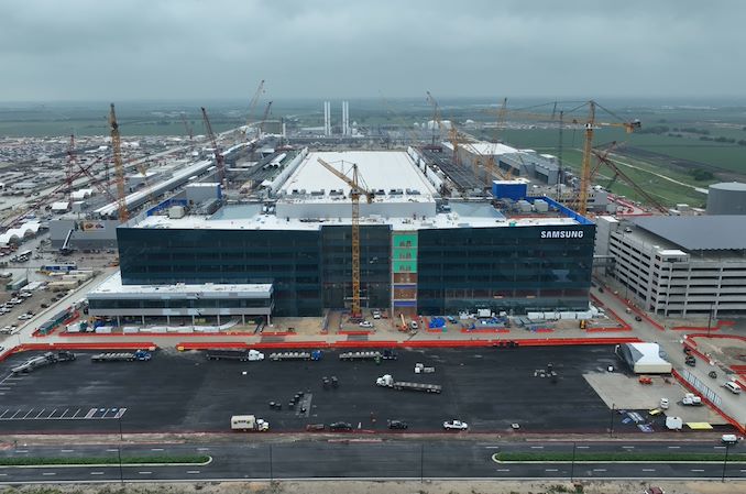
Samsung To Receive $6.4 Billion Under CHIPS Act to Build $40 Billion Fab in Texas <p align="center"><a href="https://www.anandtech.com/show/21353/samsung-to-receive-64-billion-under-chips-science-act-to-build-40-billion-fab-in-texas"><img src="https://images.anandtech.com/doci/21353/samsung-taylor-texas-office_575px.jpg" alt="" /></a></p><p><p>Samsung Electronics this week <a href="https://www.commerce.gov/news/press-releases/2024/04/biden-harris-administration-announces-preliminary-terms-samsung">was awarded</a> up to $6.4 billion from the U.S. government under the CHIPS and Science Act to build its new fab complex in Taylor, Texas. This is the third major award under the act in the last month, with all three leading-edge fabs – <a href="https://www.anandtech.com/show/21314/intel-to-get-85-billion-from-us-govt-to-build-fabs-in-the-us">Intel</a>, <a href="https://www.anandtech.com/show/21337/tsmc-to-receive-6b-us-chips-act-set-to-build-2nm-fab-in-arizona">TSMC</a>, and now Samsung – receiving multi-billion dollar funding packages under the domestic chip production program. Overall, the final price tag on Samsung's new fab complex is expected to reach $40 billion by the time it's completed later this decade.</p>
<p>Samsung's CHIPS Act funding was announced during a celebratory event attended by U.S. Secretary of Commerce Gina Raimondo and Samsung Semiconductor chief executive Kye Hyun Kyung. During the event, Kyung outlined the strategic goals of the expansion, emphasizing that the additional funding will not only increase production capacity but also strengthen the entire local semiconductor ecosystem. Samsung plans to equip its fab near Taylor, Texas, with the latest wafer fab tools to produce advanced chips. The Financial Times reports that Samsung aims to produce semiconductors on its 2nm-class process technology starting 2026, though for now this is unofficial information.</p>
<p>"I am pleased to announce a preliminary agreement between Samsung and the Department of Commerce to bring Samsung's advanced semiconductor manufacturing and research and development to Texas," <a href="https://www.whitehouse.gov/briefing-room/statements-releases/2024/04/15/statement-from-president-joe-biden-on-chips-and-science-act-preliminary-agreement-with-samsung/">said</a> Joe Biden, the U.S. president, in a statement. "This announcement will unleash over $40 billion in investment from Samsung, and cement central Texas's role as a state-of-the-art semiconductor ecosystem, creating at least 21,500 jobs and leveraging up to $40 million in CHIPS funding to train and develop the local workforce. These facilities will support the production of some of the most powerful chips in the world, which are essential to advanced technologies like artificial intelligence and will bolster U.S. national security."</p>
<p>Samsung has been a significant contributor to the Texas economy for decades, starting chip manufacturing in the U.S. in 1996. With previous investments totaling $18 billion in its Austin operations, Samsung's expansion into Taylor with an additional investment of at least $17 billion underscores its role as one of the largest foreign direct investors in U.S. history. The total expected investment in the new fab surpasses $40 billion, making it one of the largest for a greenfield project in the nation and transforming Taylor into a major hub for semiconductor manufacturing.</p>
<p>The CEO highlighted the substantial economic impact of Samsung's operations, noting a nearly double increase in regional economic output from $13.6 billion to $26.8 billion between 2022 and 2023. The ongoing expansion is projected to further stimulate economic growth, create thousands of jobs, and enhance the community's overall development.</p>
<p>“We are not just expanding production facilities; we’re strengthening the local semiconductor ecosystem and positioning the U.S. as a global semiconductor manufacturing destination.” said Kyung. “To meet the expected surge in demand from U.S. customers, for future products like AI chips, our fabs will be equipped for cutting-edge process technologies and help bring security to the U.S. semiconductor supply chain.”</p>
<p>Samsung is also committed to environmental sustainability and workforce development. The company plans to operate using 100% clean energy and incorporate advanced water management technologies. Additionally, it is investing in education and training programs to develop a new generation of semiconductor professionals. These initiatives include partnerships with educational institutions and programs tailored for military veterans.</p>
<p>In his remarks, Kyung expressed gratitude to President Biden, Secretary Raimondo, and other governmental and community supporters for their ongoing support. This collaborative effort between Samsung and various levels of government, as well as the local community, is pivotal in advancing America's... Semiconductors
Samsung To Receive $6.4 Billion Under CHIPS Act to Build $40 Billion Fab in Texas
Samsung Electronics this week was awarded up to $6.4 billion from the U.S. government under the CHIPS and Science Act to build its new fab complex in Taylor, Texas. This is the third major award under the act in the last month, with all three leading-edge fabs – Intel, TSMC, and now Samsung – receiving multi-billion dollar funding packages under the domestic chip production program. Overall, the final price tag on Samsung's new fab complex is expected to reach $40 billion by the time it's completed later this decade.
Samsung's CHIPS Act funding was announced during a celebratory event attended by U.S. Secretary of Commerce Gina Raimondo and Samsung Semiconductor chief executive Kye Hyun Kyung. During the event, Kyung outlined the strategic goals of the expansion, emphasizing that the additional funding will not only increase production capacity but also strengthen the entire local semiconductor ecosystem. Samsung plans to equip its fab near Taylor, Texas, with the latest wafer fab tools to produce advanced chips. The Financial Times reports that Samsung aims to produce semiconductors on its 2nm-class process technology starting 2026, though for now this is unofficial information.
"I am pleased to announce a preliminary agreement between Samsung and the Department of Commerce to bring Samsung's advanced semiconductor manufacturing and research and development to Texas," said Joe Biden, the U.S. president, in a statement. "This announcement will unleash over $40 billion in investment from Samsung, and cement central Texas's role as a state-of-the-art semiconductor ecosystem, creating at least 21,500 jobs and leveraging up to $40 million in CHIPS funding to train and develop the local workforce. These facilities will support the production of some of the most powerful chips in the world, which are essential to advanced technologies like artificial intelligence and will bolster U.S. national security."
Samsung has been a significant contributor to the Texas economy for decades, starting chip manufacturing in the U.S. in 1996. With previous investments totaling $18 billion in its Austin operations, Samsung's expansion into Taylor with an additional investment of at least $17 billion underscores its role as one of the largest foreign direct investors in U.S. history. The total expected investment in the new fab surpasses $40 billion, making it one of the largest for a greenfield project in the nation and transforming Taylor into a major hub for semiconductor manufacturing.
The CEO highlighted the substantial economic impact of Samsung's operations, noting a nearly double increase in regional economic output from $13.6 billion to $26.8 billion between 2022 and 2023. The ongoing expansion is projected to further stimulate economic growth, create thousands of jobs, and enhance the community's overall development.
“We are not just expanding production facilities; we’re strengthening the local semiconductor ecosystem and positioning the U.S. as a global semiconductor manufacturing destination.” said Kyung. “To meet the expected surge in demand from U.S. customers, for future products like AI chips, our fabs will be equipped for cutting-edge process technologies and help bring security to the U.S. semiconductor supply chain.”
Samsung is also committed to environmental sustainability and workforce development. The company plans to operate using 100% clean energy and incorporate advanced water management technologies. Additionally, it is investing in education and training programs to develop a new generation of semiconductor professionals. These initiatives include partnerships with educational institutions and programs tailored for military veterans.
In his remarks, Kyung expressed gratitude to President Biden, Secretary Raimondo, and other governmental and community supporters for their ongoing support. This collaborative effort between Samsung and various levels of government, as well as the local community, is pivotal in advancing America's... Semiconductors


0 Comments