


In addition to revealing its roadmap and plans concerning its current leading-edge process technologies, TSMC also shared progress of its N2 node as part of its Symposiums 2024. The company's first 2nm-class fabrication node, and predominantly featuring gate-all-around transistors, according to TSMC N2 has almost achieved its target performance and yield goals, which places it on track to enter high-volume manufacturing in the second half of 2025.
TSMC states that 'N2 development is well on track and N2P is next.' In particular, gate-all-around nanosheet devices currently achieve over 90% of their expected performance, whereas yields of 256 Mb SRAM (32 MB) devices already exceeds 80%, depending on the batch. All of this for a node that is over a year away from mass production.
Meanwhile, average yield of a 256 Mb SRAM was around 70% as of March, 2024, up from around 35% in April, 2023. Device performance has also been improving with higher frequencies being achieved while keeping power consumption in check.
Chip designer interest towards TSMC's first 2nm-class gate-all-around nanosheet transistor-based technology is significant, too. The number of new tape-outs (NTOs) in the first year of N2 is over two-times higher than it was for N5. Though with that said, given TSMC's close working relationship with a handful of high-volume vendors – most notably Appe – NTOs can be a very misleading figure since the first year of a new node at TSMC is capacity constrained, and consequently the bulk of that capacity goes to TSMC's priority partners.
Meanwhile, there were considerably more N5 tapeouts in its second year (some where N5P, of course) and N2 promises to have 2.6X more NTOs in its second year. So the node indeed looks quite promising. In fact, based on TSMC's slides (which we're unfortunately not able to republish), N2 is more popular than N3 in terms of NTOs both in the first and the second years of existence.
When it comes to the second year of N2, in the second half of 2026 TSMC plans to roll out its N2P technology, which promises additional performance and power benefits. N2P is expected to improve frequency by 15% - 20%, reduce power consumption by 30% - 40%, and increase chip density by over 1.15 times compared to N3E, significant benefits to move to all-new GAA nanosheet transistors.
Finally, for those companies that need the best in performance, power, and density, TSMC is poised to offer their A16 process in 2026. That node will also bring in backside power delivery, which will add costs, but is expected to greatly improve performance efficiency and scaling.
Semiconductors
In addition to revealing its roadmap and plans concerning its current leading-edge process technologies, TSMC also shared progress of its N2 node as part of its Symposiums 2024. The company's first 2nm-class fabrication node, and predominantly featuring gate-all-around transistors, according to TSMC N2 has almost achieved its target performance and yield goals, which places it on track to enter high-volume manufacturing in the second half of 2025.
TSMC states that 'N2 development is well on track and N2P is next.' In particular, gate-all-around nanosheet devices currently achieve over 90% of their expected performance, whereas yields of 256 Mb SRAM (32 MB) devices already exceeds 80%, depending on the batch. All of this for a node that is over a year away from mass production.
Meanwhile, average yield of a 256 Mb SRAM was around 70% as of March, 2024, up from around 35% in April, 2023. Device performance has also been improving with higher frequencies being achieved while keeping power consumption in check.
Chip designer interest towards TSMC's first 2nm-class gate-all-around nanosheet transistor-based technology is significant, too. The number of new tape-outs (NTOs) in the first year of N2 is over two-times higher than it was for N5. Though with that said, given TSMC's close working relationship with a handful of high-volume vendors – most notably Appe – NTOs can be a very misleading figure since the first year of a new node at TSMC is capacity constrained, and consequently the bulk of that capacity goes to TSMC's priority partners.
Meanwhile, there were considerably more N5 tapeouts in its second year (some where N5P, of course) and N2 promises to have 2.6X more NTOs in its second year. So the node indeed looks quite promising. In fact, based on TSMC's slides (which we're unfortunately not able to republish), N2 is more popular than N3 in terms of NTOs both in the first and the second years of existence.
When it comes to the second year of N2, in the second half of 2026 TSMC plans to roll out its N2P technology, which promises additional performance and power benefits. N2P is expected to improve frequency by 15% - 20%, reduce power consumption by 30% - 40%, and increase chip density by over 1.15 times compared to N3E, significant benefits to move to all-new GAA nanosheet transistors.
Finally, for those companies that need the best in performance, power, and density, TSMC is poised to offer their A16 process in 2026. That node will also bring in backside power delivery, which will add costs, but is expected to greatly improve performance efficiency and scaling.
Semiconductors![Rapidus Adds Chip Packaging Services to Plans for $32 Billion 2nm Fab <p align="center"><a href="https://www.anandtech.com/show/21411/rapidus-adds-chip-packaging-services-to-plans-for-32b-2nm-fab"><img src="https://images.anandtech.com/doci/21411/microsoft-azure-datacenter-custom-chip-processor-wafer-semiconductor-fab-678_575px.jpg" alt="" /></a></p><p><p>To say that the global foundry market is booming right now would be an understatement. Demand for leading-edge process technologies driven by AI and HPC applications is unprecedented, and with Intel joining the contract chipmaking game, this market segment is once again becoming rather competitive as well. Yet, this is exactly the market segment that Rapidus, a foundry startup backed by the Japanese government and several major Japanese companies, is going to enter in 2027, when its first fab comes online, just a few years from now.</p>
<p>In a fresh update on the status of bringing up the company's first leading-edge fab, Rapidus has revealed that they are intending to get in to the chip packaging game as well. Once complete, the ¥5 trillion ($32 billion) fab will be offering both chip lithography on a 2nm node, as well as packaging services for chips produced within the facility – a notable distinction in an industry where, even if packaging isn't outsourced entirely (OSAT), it's still normally handled at dedicated facilities.</p>
<p>Ultimately, while the company wants to serve the same clients as TSMC, Samsung, and Intel Foundry, the firm plans to do things almost completely differently than its competitors in a bid to speed up chipmaking from finishing design to getting a working chip out of the fab.</p>
<p>"We are very proud of being Japanese," said Henri Richard, general manager and president of Rapidus's subsidiary in the U.S. "[…] I know that some people may be looking at this thinking [that] Japan is known for quality, attention to detail, but not necessarily for speed, or flexibility. But I will tell you that Atsuyoshi Koike (the head of Rapidus) is a very special executive. That is, he has all the quality of Japan, with a lot of American thinking. So he is quite a unique guy, and certainly extraordinarily focused on creating a company that will be extremely flexible and extremely quick on its feet."</p>
<h3>2nm Only, At First</h3>
<p>Perhaps the most significant difference between Rapidus and traditional foundries is that the company will offer only leading-edge manufacturing technologies to its clients: 2 nm in 2027 (phase 1) and then 1.4 nm in the future (phase 2). This is a stark contrast with other contract fabs, including Intel, which tend to offer their customers a full range of fabrication processes to land more clients and produce more chips. Apparently, Rapidus hopes that that there will be enough Japanese and American chip developers that are inclined to use its 2 nm fabrication process to produce their designs. With that said, the number of chip designers that are using the most advanced production node at any given time is relatively small – limited to large firms who need first-mover advantage and have the margins to justify taking the risk – so it remains to be seen whether Rapidus's business model becomes successful. The company believes it will, since the market of chips made on advanced nodes is growing rapidly.</p>
<p>"Until recently IDC was giving a an estimation of the 2nm and below market as about $80 billion and I think we are going to see soon a revision of the potential to $150 billion," said Richard. "[…] TSMC is the 800 pound gorilla in the space. Samsung is there and Intel is going to enter that space. But the market growth is so significant and the demand is so high, that it does not take a lot of market share for Rapidus to be successful. One of the things that gives me great comfort is that when I talk to our EDA partners, when I talk to our potential clients, it is obvious that the entire industry is looking for alternative supply from a fully independent foundry. There is a place for Samsung in this industry, there is a place for Intel in this industry, the industry is currently owned by TSMC. But another totally independent foundry is more than welcome by all of the ecosystem partners and by the customers. So, I feel really, really good about Rapidus's positioning."</p>
<p>Speaking of advanced process technologies, it is notable that Rapidus does not plan to use ASML's High-NA Twinscan EXE lithography scanners for 2 nm production. Instead, Rapidus is sticking to ASML's proven Low-NA scanners, which will reduce costs of Rapidus's fab, though it will entail usage of EUV double patterning, which brings up costs and lengthens the production cycle in other ways. Even with those trade-offs, <a href="https://www.semianalysis.com/p/asml-dilemma-high-na-euv-is-worse">SemiAnalysis analysts believe</a> that given the cost of High-NA EUV litho tools and halved imaging field, ... Semiconductors](https://lh3.googleusercontent.com/blogger_img_proxy/AEn0k_sHQqAyHmuyBWmIhKEQY4sxC1Yi3FJ-76qttv-bMnnydLF3PdSwsX2tysiLpRIxQw9InB3MI7Ya8C1rDitfcQjT3JDCvf9exbH1KTZYWESa0IczjTJ1skSc5shJZ36ZAapAC3YO_pWsDETeApsjxi73rxXZaBQpPuSMtsQIf0kLXkkqUXiFBRWDsqz73lCPymqdZeshtpdchvWdl1snUgll4Q=w72-h72-p-k-no-nu)
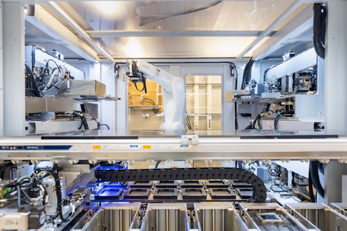
To say that the global foundry market is booming right now would be an understatement. Demand for leading-edge process technologies driven by AI and HPC applications is unprecedented, and with Intel joining the contract chipmaking game, this market segment is once again becoming rather competitive as well. Yet, this is exactly the market segment that Rapidus, a foundry startup backed by the Japanese government and several major Japanese companies, is going to enter in 2027, when its first fab comes online, just a few years from now.
In a fresh update on the status of bringing up the company's first leading-edge fab, Rapidus has revealed that they are intending to get in to the chip packaging game as well. Once complete, the ¥5 trillion ($32 billion) fab will be offering both chip lithography on a 2nm node, as well as packaging services for chips produced within the facility – a notable distinction in an industry where, even if packaging isn't outsourced entirely (OSAT), it's still normally handled at dedicated facilities.
Ultimately, while the company wants to serve the same clients as TSMC, Samsung, and Intel Foundry, the firm plans to do things almost completely differently than its competitors in a bid to speed up chipmaking from finishing design to getting a working chip out of the fab.
"We are very proud of being Japanese," said Henri Richard, general manager and president of Rapidus's subsidiary in the U.S. "[…] I know that some people may be looking at this thinking [that] Japan is known for quality, attention to detail, but not necessarily for speed, or flexibility. But I will tell you that Atsuyoshi Koike (the head of Rapidus) is a very special executive. That is, he has all the quality of Japan, with a lot of American thinking. So he is quite a unique guy, and certainly extraordinarily focused on creating a company that will be extremely flexible and extremely quick on its feet."
Perhaps the most significant difference between Rapidus and traditional foundries is that the company will offer only leading-edge manufacturing technologies to its clients: 2 nm in 2027 (phase 1) and then 1.4 nm in the future (phase 2). This is a stark contrast with other contract fabs, including Intel, which tend to offer their customers a full range of fabrication processes to land more clients and produce more chips. Apparently, Rapidus hopes that that there will be enough Japanese and American chip developers that are inclined to use its 2 nm fabrication process to produce their designs. With that said, the number of chip designers that are using the most advanced production node at any given time is relatively small – limited to large firms who need first-mover advantage and have the margins to justify taking the risk – so it remains to be seen whether Rapidus's business model becomes successful. The company believes it will, since the market of chips made on advanced nodes is growing rapidly.
"Until recently IDC was giving a an estimation of the 2nm and below market as about $80 billion and I think we are going to see soon a revision of the potential to $150 billion," said Richard. "[…] TSMC is the 800 pound gorilla in the space. Samsung is there and Intel is going to enter that space. But the market growth is so significant and the demand is so high, that it does not take a lot of market share for Rapidus to be successful. One of the things that gives me great comfort is that when I talk to our EDA partners, when I talk to our potential clients, it is obvious that the entire industry is looking for alternative supply from a fully independent foundry. There is a place for Samsung in this industry, there is a place for Intel in this industry, the industry is currently owned by TSMC. But another totally independent foundry is more than welcome by all of the ecosystem partners and by the customers. So, I feel really, really good about Rapidus's positioning."
Speaking of advanced process technologies, it is notable that Rapidus does not plan to use ASML's High-NA Twinscan EXE lithography scanners for 2 nm production. Instead, Rapidus is sticking to ASML's proven Low-NA scanners, which will reduce costs of Rapidus's fab, though it will entail usage of EUV double patterning, which brings up costs and lengthens the production cycle in other ways. Even with those trade-offs, SemiAnalysis analysts believe that given the cost of High-NA EUV litho tools and halved imaging field, ... Semiconductors

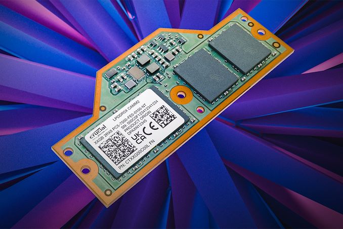
As LPCAMM2 adoption begins, the first retail memory modules are finally starting to hit the retail market, courtesy of Micron. The memory manufacturer has begun selling their LPDDR5X-based LPCAMM2 memory modules under their in-house Crucial brand, making them available on the latter's storefront. Timed to coincide with the release of Lenovo's ThinkPad P1 Gen 7 laptop – the first retail laptop designed to use the memory modules – this marks the de facto start of the eagerly-awaited modular LPDDR5X memory era.
Micron's Low Power Compression Attached Memory Module 2 (LPCAMM2) modules are available in capacities of 32 GB and 64 GB. These are dual-channel modules that feature a 128-bit wide interface, and are based around LPDDR5X memory running at data rates up to 7500 MT/s. This gives a single LPCAMM2 a peak bandwidth of 120 GB/s. Micron is not disclosing the latencies of its LPCAMM2 memory modules, but it says that high data transfer rates of LPDDR5X compensate for the extended timings.
Micron says that LPDDR5X memory offers significantly lower power consumption, with active power per 64-bit bus being 43-58% lower than DDR5 at the same speed, and standby power up to 80% lower. Meanwhile, similar to DDR5 modules, LPCAMM2 modules include a power management IC and voltage regulating circuitry, which provides module manufacturers additional opportunities to reduce power consumption of their products.
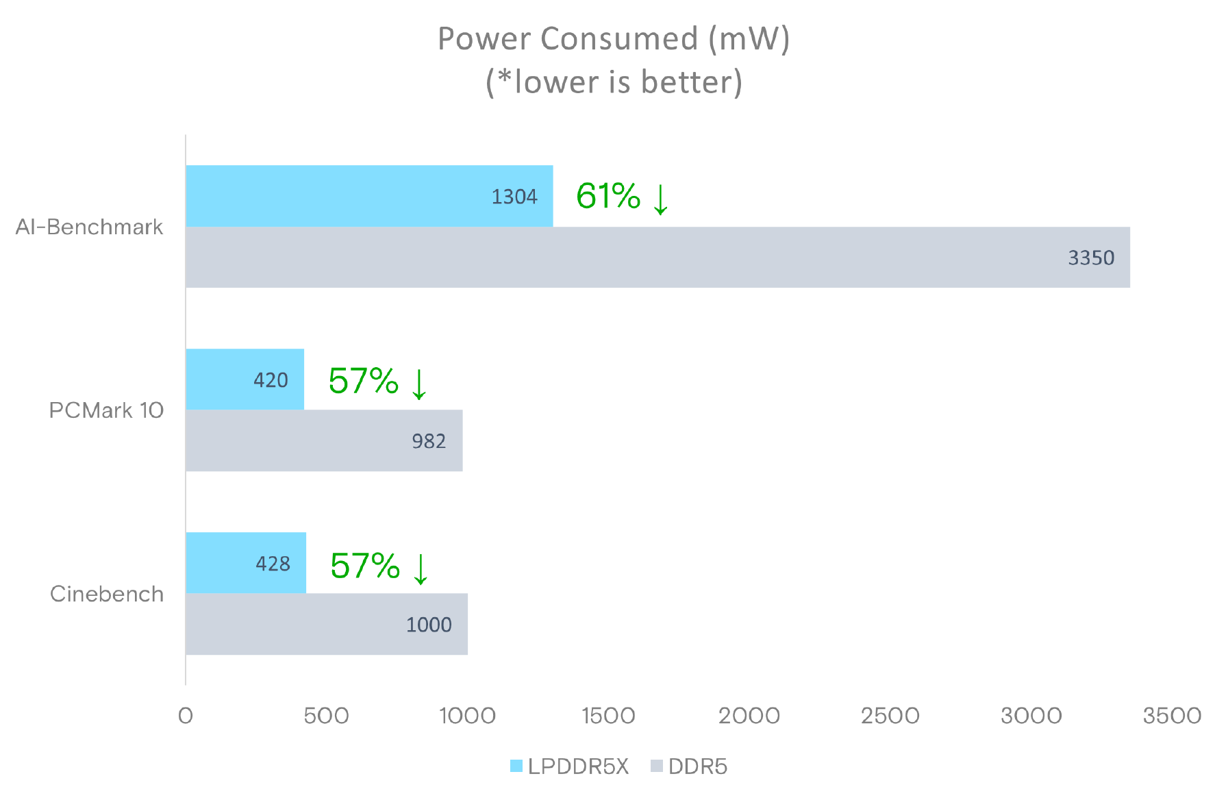
Source: Micron LPDDR5X LPCAMM2 Technical Brief
It's worth noting, however, that at least for the first generation of LPCAMM2 modules, system vendors will need to pick between modularity and performance. While soldered-down LPDDR5X memory is available at speeds up to 8533 MT/sec – and with 9600 MT/sec on the horizon – the fastest LPCAMM2 modules planned for this year by both Micron and rival Samsung will be running at 7500 MT/sec. So vendors will have to choose between the flexibility of offering modular LPDDR5X, or the higher bandwidth (and space savings) offered by soldering down their memory.
Micron, for its part, is projecting that 9600 MT/sec LPCAMM2 modules will be available by 2026. Though it's all but certain that faster memory will also be avaialble in the same timeframe.
Micron's Crucial LPDDR5X 32 GB module costs $174.99, whereas a 64 GB module costs $329.99.
Memory
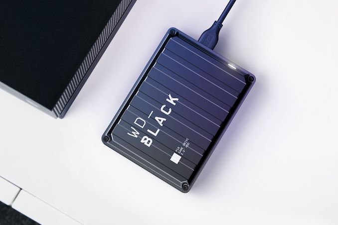
UPDATE 5/17, 6 PM: Western Digital has confirmed that the new 2.5-inch T GB HDDs uses 6 SMR platters
The vast majority of laptops nowadays use solid-state drives, which is why the development of new, higher-capacity 2.5-inch hard drives has all but come to a halt. Or rather, it almost has. It seems that the 2.5-inch form factor has a bit more life left in it after all, as today Western Digital has released a slate of new external storage products based on a new, high-capacity 6 TB 2.5-inch hard drive.
WD's new 6 TB spinner is being used to offer upgraded versions of the company's My Passport, Black P10, and and G-DRIVE ArmorATD portable storage products. Notably, however, WD isn't selling the bare 2.5-inch drive on a standalone basis – at least not yet – so for the time being it's entirely reserved for use in external storage.
Consequently, WD isn't publishing much about the 6 TB hard drive itself. The maximum read speed for these products is listed at 130 MB/sec – the same as WD's existing externals – and write performance goes unmentioned.
Notably, all of these 6 TB devices are thicker than their existing 5 TB counterparts, which strongly suggests that WD has increased their storage capacity not by improving their areal density, but by adding another platter to their existing drive platform (which WD has since confirmed). This, in turn, would help to explain why these new drives are being used in external storage products, as WD's 5 TB 2.5-inch drives are already 15mm thick and using 5 platters. 15mm is the highest standard thickness for a 2.5-inch form-factor, and already incompatible with a decent number of portable devices. External drives, in turn, are the only place these even thicker 2.5-inch drives would fit.
WD's specifications also gloss over whether these drives are based on shingled magnetic recording (SMR) technology. The company was already using SMR for their 5 TB drives in order to hit the necessary storage density there, and WD has since confirmed that this is exactly the case. Which is likely why the company isn't publishing write performance specifications for the drives, as we've seen device-managed SMR drives bottom out as low as 10 MB/second in our testing when the drive needs to rewrite data.
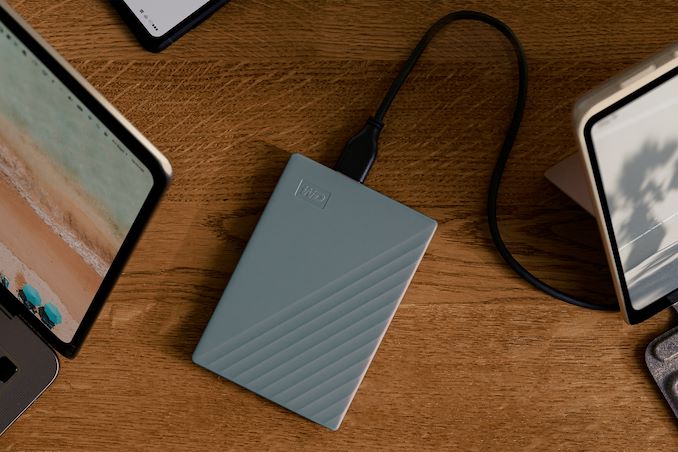
Depending on the specific drive model, all of the external storage drives use either a USB-C connector, or the very quaint USB Micro-B 3.0 connector. Though regardless of the physical connector used, all of the drives feature a USB 3.2 Gen 1 (5Gbps) electrical interface, which is more than ample given the drives' physically-limited transfer speeds.
Wrapping things up, according to WD the new drives are available at retail immediately. The WD My Passport Ultra and WD My Passport Ultra for Mac with USB-C both retail for $199.99; the WD My Passport and WD My Passport for Mac are $179.99; the WD My Passport Works With USB-C is $184.99; the gaming-focused WD_Black P10 Game Drive sells for $184.99, and the SanDisk Professional G-Drive ArmorATD is $229.99. All of Western Digital's external storage drives are backed with a three-year limited warranty.
Storage
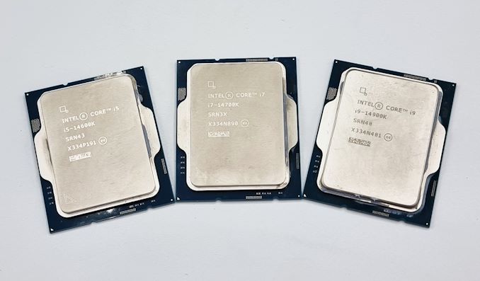
Further to our last piece which we detailed Intel's issue to motherboard vendors to follow with stock power settings for Intel's 14th and 13th Gen Core series processors, Intel has now issued a follow-up statement to this. Over the last week or so, motherboard vendors quickly released firmware updates with a new profile called 'Intel Baseline', which motherboard vendors assumed would address the instability issues.
As it turns out, Intel doesn't seem to accept this as technically, these Intel Baseline profiles are not to be confused with Intel's default specifications. This means that Intel's Baseline profiles seemingly give the impression that they are operating at default settings, hence the terminology 'baseline' used, but this still opens motherboard vendors to use their interpretations of MCE or Multi-Core Enhancement.
To clarify things for consumers, Intel has sent us the following statement:
Several motherboard manufacturers have released BIOS profiles labeled ‘Intel Baseline Profile’. However, these BIOS profiles are not the same as the 'Intel Default Settings' recommendations that Intel has recently shared with its partners regarding the instability issues reported on 13th and 14th gen K SKU processors.
These ‘Intel Baseline Profile’ BIOS settings appear to be based on power delivery guidance previously provided by Intel to manufacturers describing the various power delivery options for 13th and 14th Generation K SKU processors based on motherboard capabilities.
Intel is not recommending motherboard manufacturers to use ‘baseline’ power delivery settings on boards capable of higher values.
Intel’s recommended ‘Intel Default Settings’ are a combination of thermal and power delivery features along with a selection of possible power delivery profiles based on motherboard capabilities.
Intel recommends customers to implement the highest power delivery profile compatible with each individual motherboard design as noted in the table below:
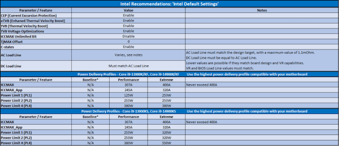
Click to Enlarge Intel's Default Settings
What Intel's statement is effectively saying to consumers, is that users shouldn't be using the Baseline Power Delivery profiles which are offered by motherboard vendors through a plethora of firmware updates. Instead, Intel is recommending users opt for Intel Default Settings, which follows what the specific processor is rated for by Intel out of the box to achieve the clock speeds advertised, without users having to worry about firmware 'over' optimization which can cause instability as there have been many reports of happening.
Not only this, but the Intel Default settings offer a combination of thermal specifications and power capabilities, including voltage and frequency curve settings that apply to the capability of the motherboard used, and the power delivery equipped on the motherboard. At least for the most part, Intel is recommending users with 14th and 13th-Gen Core series K, KF, and KS SKUs that they do not recommend users opt in using the Baseline profiles offered by motherboard vendors.
Digesting the contrast between the two statements, the key differential is that Intel's priority is reducing the current going through the processor, which for both the 14th and 13th Gen Core series processors is a maximum of 400 A, even when using the Extreme profile. We know those motherboard vendors on their Z790 and Z690 motherboards opt for an unrestricted power profile, which is essentially 'unlimited' power and current to maximize performance at the cost of power consumption and heat, which does exacerbate problems and can lead to frequent bouts of instability, especially on high-intensity workloads.
Another variable Intel is recommending is that the AC Load Line must match the design target of the processor, with a maximum value of 1.1 mOhm, and that the DC Load Line must be ... CPUs
Further to our last piece which we detailed Intel's issue to motherboard vendors to follow with stock power settings for Intel's 14th and 13th Gen Core series processors, Intel has now issued a follow-up statement to this. Over the last week or so, motherboard vendors quickly released firmware updates with a new profile called 'Intel Baseline', which motherboard vendors assumed would address the instability issues.
As it turns out, Intel doesn't seem to accept this as technically, these Intel Baseline profiles are not to be confused with Intel's default specifications. This means that Intel's Baseline profiles seemingly give the impression that they are operating at default settings, hence the terminology 'baseline' used, but this still opens motherboard vendors to use their interpretations of MCE or Multi-Core Enhancement.
To clarify things for consumers, Intel has sent us the following statement:
Several motherboard manufacturers have released BIOS profiles labeled ‘Intel Baseline Profile’. However, these BIOS profiles are not the same as the 'Intel Default Settings' recommendations that Intel has recently shared with its partners regarding the instability issues reported on 13th and 14th gen K SKU processors.
These ‘Intel Baseline Profile’ BIOS settings appear to be based on power delivery guidance previously provided by Intel to manufacturers describing the various power delivery options for 13th and 14th Generation K SKU processors based on motherboard capabilities.
Intel is not recommending motherboard manufacturers to use ‘baseline’ power delivery settings on boards capable of higher values.
Intel’s recommended ‘Intel Default Settings’ are a combination of thermal and power delivery features along with a selection of possible power delivery profiles based on motherboard capabilities.
Intel recommends customers to implement the highest power delivery profile compatible with each individual motherboard design as noted in the table below:
Click to Enlarge Intel's Default Settings
What Intel's statement is effectively saying to consumers, is that users shouldn't be using the Baseline Power Delivery profiles which are offered by motherboard vendors through a plethora of firmware updates. Instead, Intel is recommending users opt for Intel Default Settings, which follows what the specific processor is rated for by Intel out of the box to achieve the clock speeds advertised, without users having to worry about firmware 'over' optimization which can cause instability as there have been many reports of happening.
Not only this, but the Intel Default settings offer a combination of thermal specifications and power capabilities, including voltage and frequency curve settings that apply to the capability of the motherboard used, and the power delivery equipped on the motherboard. At least for the most part, Intel is recommending users with 14th and 13th-Gen Core series K, KF, and KS SKUs that they do not recommend users opt in using the Baseline profiles offered by motherboard vendors.
Digesting the contrast between the two statements, the key differential is that Intel's priority is reducing the current going through the processor, which for both the 14th and 13th Gen Core series processors is a maximum of 400 A, even when using the Extreme profile. We know those motherboard vendors on their Z790 and Z690 motherboards opt for an unrestricted power profile, which is essentially 'unlimited' power and current to maximize performance at the cost of power consumption and heat, which does exacerbate problems and can lead to frequent bouts of instability, especially on high-intensity workloads.
Another variable Intel is recommending is that the AC Load Line must match the design target of the processor, with a maximum value of 1.1 mOhm, and that the DC Load Line must be ... CPUs
![TSMC Offers a Peek at 'Global Gigafab' Process Replication Program <p align="center"><a href="https://www.anandtech.com/show/21407/tsmc-offers-peek-at-global-gigafab-process-replication-program"><img src="https://images.anandtech.com/doci/21407/tsmc_wafer_semiconductor_chip_300mm_fab_2_575px.jpg" alt="" /></a></p><p><p>At its European Technology Symposium last week TSMC revealed some of the details about its Global Gigafab Manufacturing program, the company's strategy to replicate its manufacturing processes across its multiple gigafab sites.</p>
<p>The need for large-scale multi-national fabs to have a process in place to replicate their facilities is well-documented at this point. As scaling-up at at the gigafab size means scaling-out instead, chip makers need to be able to quickly get new and updated manufacturing processes ported to other facilities in order to hit their necessary throughput – and to avoid a multi-quarter bottlenecks that come from having to freshly-tune a fab.</p>
<p>Intel, for their part, has a well-known Copy Exactly program, which is one of the company's major competitive advantages, allowing it to share process recipes across its fabs around the world to maximize yields and reduce performance variability. Meanwhile, as Taiwan Semiconductor Manufacturing Co. is building additional capacity in different parts of the world, it has reached the point where it needs a similar program in order to quickly maximize its yields and productivity at its new fabs in Japan and the U.S. And in some respects, TSMC's program goes even further than Intel's, with an additional focus on sustainability and social responsibility.</p>
<p>"As mentioned at last year's symposium, [Global Gigafab manufacturing] is a powerful global manufacturing and management platform," said Y.L. Wang, Vice President of Fab Operations TSMC. "We realise one fab management to ensure our Gigafab to achieve consistent operation efficiency as well as production quality on a global scale. Moreover, we also pursue sustainability across our global footprint covering green manufacturing, global talent development, supply chain localization, as well as social responsibility."</p>
<table align="center" border="0" cellpadding="0" cellspacing="1" width="650">
<tbody>
<tr class="tgrey">
<td align="center" colspan="4">TSMC's Global GigaFab Manufacturing<br />
Data by TSMC (Compiled by AnandTech)</td>
</tr>
<tr class="tlblue">
<td align="center" valign="middle" width="137">Manufacturing Excellence</td>
<td align="center" valign="middle" width="137">Sustainability</td>
</tr>
<tr>
<td align="center" valign="middle">Global One Fab Manufacturing</td>
<td align="center" valign="middle">Green Manufacturing</td>
</tr>
<tr>
<td align="center" valign="middle">ML-based Process Control</td>
<td align="center" valign="middle">Global Talent Development</td>
</tr>
<tr>
<td align="center" valign="middle">Manufacturing Agility and Quality</td>
<td align="center" valign="middle">Supply Chain Localization</td>
</tr>
<tr>
<td align="center" valign="middle">Maximum Productivity</td>
<td align="center" valign="middle">Social Responsibility</td>
</tr>
</tbody>
</table>
<p>When it comes to improvements of process technology, there are two main mechanisms: the continuous process improvements (CPI) to improve yields, as well as statistical process control (SPC) reduce performance variations. To do so, the company has multiple internal techniques that rely on machine learning-based process control, constant quality measuring, and various productivity improving methods. With Global Gigafab manufacturing TSMC can use CPI and SPC to improve yields and performance on the global scale by sharing knowledge between different sites.</p>
<p>"When we port a technology from Taiwan to Arizona, the fab set up, the process control system, everything is actually a copy from Taiwan," said Kevin Zhang, Senior Vice President, Business Development and Overseas Operations Office, and Deputy Co-COO at TSMC.</p>
<p>TSMC yet has to start making chips at its fabs in Germany, Japan, and the United States, so it remains to be seen how fast the foundry will increase yields to Taiwanese levels at its Fab 23 (in Kumamoto, Japan) and Fab 21 (in Arizona) when they begin operations in 2024 and 2025, but with Global Gigafab Manufacturing program in place, this is likely set to happen rather sooner than later.</p>
</p> Semiconductors](https://lh3.googleusercontent.com/blogger_img_proxy/AEn0k_vquRlSfOxMcP78E-dA_fW32cM8-_aEhZtHNl-rnFv46VFZ4J7xOEFTnXdRos7pZbBRKg4BtQbw9EciLXfA22U_vjH1xgSvd1LkoGkq4G4c513g8qv_9oII5fCfSCRjE23jhGNOx0FqJa6QHCauLx6RrkmNunVFUKtfKHafQw=w72-h72-p-k-no-nu)
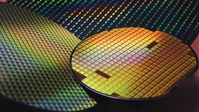
At its European Technology Symposium last week TSMC revealed some of the details about its Global Gigafab Manufacturing program, the company's strategy to replicate its manufacturing processes across its multiple gigafab sites.
The need for large-scale multi-national fabs to have a process in place to replicate their facilities is well-documented at this point. As scaling-up at at the gigafab size means scaling-out instead, chip makers need to be able to quickly get new and updated manufacturing processes ported to other facilities in order to hit their necessary throughput – and to avoid a multi-quarter bottlenecks that come from having to freshly-tune a fab.
Intel, for their part, has a well-known Copy Exactly program, which is one of the company's major competitive advantages, allowing it to share process recipes across its fabs around the world to maximize yields and reduce performance variability. Meanwhile, as Taiwan Semiconductor Manufacturing Co. is building additional capacity in different parts of the world, it has reached the point where it needs a similar program in order to quickly maximize its yields and productivity at its new fabs in Japan and the U.S. And in some respects, TSMC's program goes even further than Intel's, with an additional focus on sustainability and social responsibility.
"As mentioned at last year's symposium, [Global Gigafab manufacturing] is a powerful global manufacturing and management platform," said Y.L. Wang, Vice President of Fab Operations TSMC. "We realise one fab management to ensure our Gigafab to achieve consistent operation efficiency as well as production quality on a global scale. Moreover, we also pursue sustainability across our global footprint covering green manufacturing, global talent development, supply chain localization, as well as social responsibility."
| TSMC's Global GigaFab Manufacturing Data by TSMC (Compiled by AnandTech) |
|||
| Manufacturing Excellence | Sustainability | ||
| Global One Fab Manufacturing | Green Manufacturing | ||
| ML-based Process Control | Global Talent Development | ||
| Manufacturing Agility and Quality | Supply Chain Localization | ||
| Maximum Productivity | Social Responsibility | ||
When it comes to improvements of process technology, there are two main mechanisms: the continuous process improvements (CPI) to improve yields, as well as statistical process control (SPC) reduce performance variations. To do so, the company has multiple internal techniques that rely on machine learning-based process control, constant quality measuring, and various productivity improving methods. With Global Gigafab manufacturing TSMC can use CPI and SPC to improve yields and performance on the global scale by sharing knowledge between different sites.
"When we port a technology from Taiwan to Arizona, the fab set up, the process control system, everything is actually a copy from Taiwan," said Kevin Zhang, Senior Vice President, Business Development and Overseas Operations Office, and Deputy Co-COO at TSMC.
TSMC yet has to start making chips at its fabs in Germany, Japan, and the United States, so it remains to be seen how fast the foundry will increase yields to Taiwanese levels at its Fab 23 (in Kumamoto, Japan) and Fab 21 (in Arizona) when they begin operations in 2024 and 2025, but with Global Gigafab Manufacturing program in place, this is likely set to happen rather sooner than later.
Semiconductors
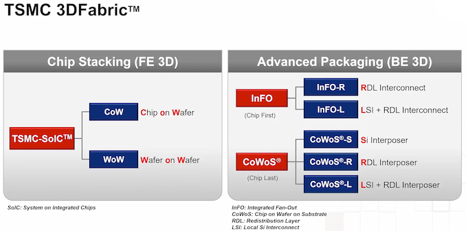
Customer demand for AI and HPC processors is driving a much greater use of advanced packaging technologies, particularly TSMC's chip-on-wafer-on-substrate (CoWoS) services. As things stand, TSMC is just barely meeting the current demand for this packaging method – never mind future demand – which is why last year the company announced plans to more than double CoWoS capacity by the end of 2024. But as it turns out, just doubling capacity once won't be enough, and the world's largest contract maker of chips is going to have to keep scaling up at a rapid pace.
At its European Technology Symposium last week TSMC announced plans to expand CoWoS capacity at a compound annual growth rate (CAGR) of over 60% till at least 2026. As a result, TSMC's CoWoS capacity will more than quadruple from 2023 levels by the end of that period. And keeping in mind that TSMC is prepping additional versions of CoWoS (namely CoWoS-L) that will enable building system-in-packages (SiPs) of up to eight reticle sizes, increasing CoWoS capacity by four-fold in three years may still not be enough. The good news is that the various third-party off-site assembly and testing (OSAT) providers are also expanding their CoWoS-like capacity, so the demand for advanced packing isn't a problem that TSMC is facing (or resolving) on their own.
And CoWoS isn't the only advanced packaging technology line whose capacity TSMC is looking to rapidly expand. The company also has its system-on-integrated chips (SoIC) 3D stacking technology which adoption is poised to grow in the coming years. To meet demand for its SoIC packaging methods TSMC will expand SoIC capacity at a 100% compound annual growth rate by the end of 2026. As a result, SoIC capacity will grow by eight-fold from 2023 levels by late 2026.
Overall, TSMC itself expects leading-edge SiPs for demanding applications like AI and HPC will adopt both CoWoS and SoIC 3D stacking technologies in the coming years, which is why it needs to increase capacity for both methods to be able to build those highly-complex processors.
Semiconductors
In addition to revealing its roadmap and plans concerning its current leading-edge process technologies, TSMC also shared progress of its N2 node as part of its Symposiums 2024. The company's first 2nm-class fabrication node, and predominantly featuring gate-all-around transistors, according to TSMC N2 has almost achieved its target performance and yield goals, which places it on track to enter high-volume manufacturing in the second half of 2025.
TSMC states that 'N2 development is well on track and N2P is next.' In particular, gate-all-around nanosheet devices currently achieve over 90% of their expected performance, whereas yields of 256 Mb SRAM (32 MB) devices already exceeds 80%, depending on the batch. All of this for a node that is over a year away from mass production.
Meanwhile, average yield of a 256 Mb SRAM was around 70% as of March, 2024, up from around 35% in April, 2023. Device performance has also been improving with higher frequencies being achieved while keeping power consumption in check.
Chip designer interest towards TSMC's first 2nm-class gate-all-around nanosheet transistor-based technology is significant, too. The number of new tape-outs (NTOs) in the first year of N2 is over two-times higher than it was for N5. Though with that said, given TSMC's close working relationship with a handful of high-volume vendors – most notably Appe – NTOs can be a very misleading figure since the first year of a new node at TSMC is capacity constrained, and consequently the bulk of that capacity goes to TSMC's priority partners.
Meanwhile, there were considerably more N5 tapeouts in its second year (some where N5P, of course) and N2 promises to have 2.6X more NTOs in its second year. So the node indeed looks quite promising. In fact, based on TSMC's slides (which we're unfortunately not able to republish), N2 is more popular than N3 in terms of NTOs both in the first and the second years of existence.
When it comes to the second year of N2, in the second half of 2026 TSMC plans to roll out its N2P technology, which promises additional performance and power benefits. N2P is expected to improve frequency by 15% - 20%, reduce power consumption by 30% - 40%, and increase chip density by over 1.15 times compared to N3E, significant benefits to move to all-new GAA nanosheet transistors.
Finally, for those companies that need the best in performance, power, and density, TSMC is poised to offer their A16 process in 2026. That node will also bring in backside power delivery, which will add costs, but is expected to greatly improve performance efficiency and scaling.
Semiconductors
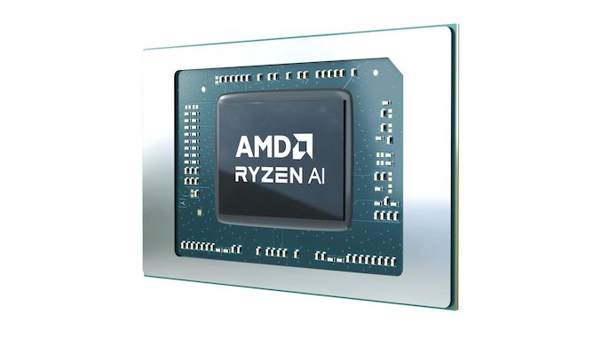
In what appears to be a mistake or a jump of the gun by ASUS, they have seemingly published a list of specifications for one of its key notebooks that all but allude to the next generation of AMD's mobile processors. While we saw AMD toy with a new nomenclature for their Phoenix silicon (Ryzen 7040 series), it seems as though AMD is once again changing things around where their naming scheme for processors is concerned.
The ASUS listing, which has now since been deleted, but as of writing is still available through Google's cache, highlights a model that is already in existence, the VivoBook S 16 OLED (M5606), but is listed with an unknown AMD Ryzen AI 9 HX 170 processor. Which, based on its specificiations, is certainly not part of the current Hawk Point (Phoenix/Phoenix 2) platform.
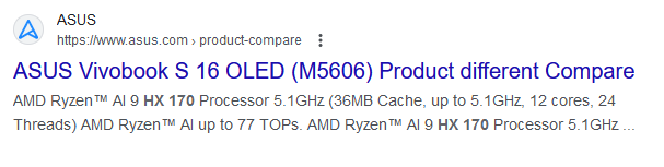
The cache on Google shows the ASUS Vivobook S 16 OLED with a Ryzen AI 9 HX 170 Processor
While it does happen in this industry occasionally, what looks like an accidental leak by ASUS on one of their product pages has unearthed an unknown processor from AMD. This first came to our attention via a post on Twitter by user @harukaze5719. While we don't speculate on rumors, we confirmed this ourselves by digging through Google's cache. Sure enough, as the image above from Google highlights, it lists a newly unannounced model of Ryzen mobile processor. Under the listing via the product compare section for the ASUS Vivobook S 16 OLED (M5606) notebook, it is listed with the AMD Ryzen AI 9 HX 170, which appears to be one of AMD's upcoming Zen 5-based mobile chips codenamed Strix Point.
So with the seemingly new nomenclature that AMD has gone with, it has a clear focus on AI, or rather Ryzen AI, by including it in the name. The Ryzen AI 9 HX 170 looks set to be a 12C/24T Zen 5 mobile variant, with their Ryzen AI NPU or similar integrated within the chip. Given that Microsoft has defined that only processors with an NPU with 45 TOPS of performance or over constitute being considered an 'AI PC', it's likely the Xilinx (now AMD Xilinx) based NPU will meet these requirements as the listing states the chip has up to 77 TOPS of AI performance available. The HX series is strikingly similar to AMD's (and Intel's) previous HX naming series for their desktop replacement SKUs for laptops, so assuming any of the details of ASUS's error are correct, then this is presumably a very high-end, high-TDP part.
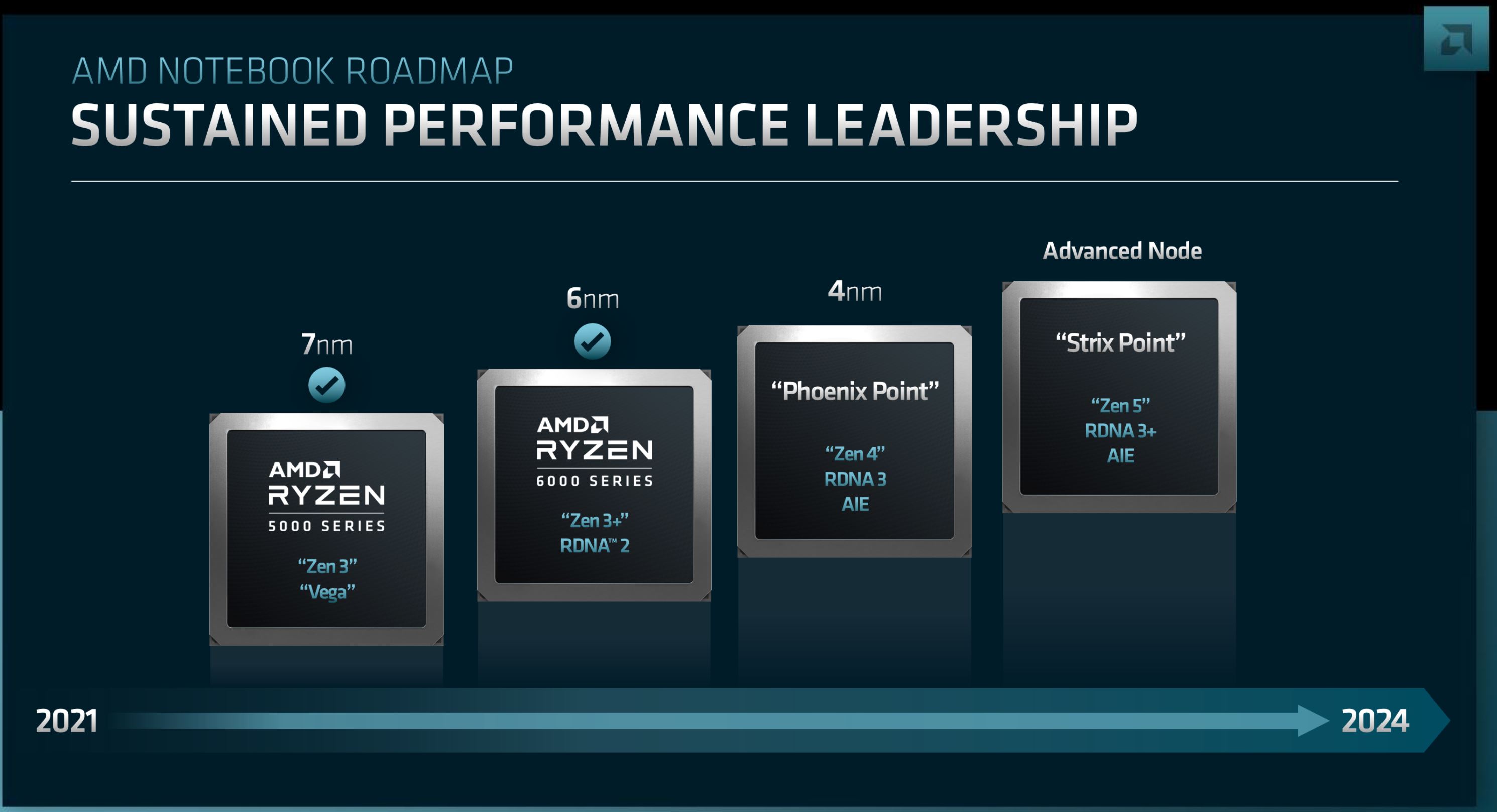
AMD Laptop Roadmap from Zen 2 in 2019 to Zen 5 on track for release in 2024
We've known for some time that AMD plans to release AMD's Zen 5-based Strix Point line-up sometime in 2024. Given the timing of Computex 2024, which is just over four weeks away, we still don't quite have the full picture of Zen 5's performance and its architectural shift over Zen 4. AMD CEO Dr. Lisa Su also confirmed that Zen 5 will come with enhanced RDNA graphics within the Strix Point SoC by stating "Strix combines our next-gen Zen 5 core with enhanced RDNA graphics and an updated Ryzen AI engine to significantly increase the performance, energy efficiency, and AI capabilities of PCs,"
While it's entirely possible as we lead up to Computex 2024 that AMD is prepared to announce more details about Zen 5, nothing is confirmed. We do know that the CEO of AMD, Dr. Lisa Su is scheduled to deliver the opening keynote of the show, Dr. Lisa Su unveiled their Zen 4 microarchitecture at Computex 2022 during AMD's keynote and even unveiled their 3D V-Cache stacking, which we know today as the Ryzen X3D CPUs back at Computex 2021.
With that in mind, AMD and Dr. Lisa Su love to announce new products and ... CPUs
Further to our last piece which we detailed Intel's issue to motherboard vendors to follow with stock power settings for Intel's 14th and 13th Gen Core series processors, Intel has now issued a follow-up statement to this. Over the last week or so, motherboard vendors quickly released firmware updates with a new profile called 'Intel Baseline', which motherboard vendors assumed would address the instability issues.
As it turns out, Intel doesn't seem to accept this as technically, these Intel Baseline profiles are not to be confused with Intel's default specifications. This means that Intel's Baseline profiles seemingly give the impression that they are operating at default settings, hence the terminology 'baseline' used, but this still opens motherboard vendors to use their interpretations of MCE or Multi-Core Enhancement.
To clarify things for consumers, Intel has sent us the following statement:
Several motherboard manufacturers have released BIOS profiles labeled ‘Intel Baseline Profile’. However, these BIOS profiles are not the same as the 'Intel Default Settings' recommendations that Intel has recently shared with its partners regarding the instability issues reported on 13th and 14th gen K SKU processors.
These ‘Intel Baseline Profile’ BIOS settings appear to be based on power delivery guidance previously provided by Intel to manufacturers describing the various power delivery options for 13th and 14th Generation K SKU processors based on motherboard capabilities.
Intel is not recommending motherboard manufacturers to use ‘baseline’ power delivery settings on boards capable of higher values.
Intel’s recommended ‘Intel Default Settings’ are a combination of thermal and power delivery features along with a selection of possible power delivery profiles based on motherboard capabilities.
Intel recommends customers to implement the highest power delivery profile compatible with each individual motherboard design as noted in the table below:
Click to Enlarge Intel's Default Settings
What Intel's statement is effectively saying to consumers, is that users shouldn't be using the Baseline Power Delivery profiles which are offered by motherboard vendors through a plethora of firmware updates. Instead, Intel is recommending users opt for Intel Default Settings, which follows what the specific processor is rated for by Intel out of the box to achieve the clock speeds advertised, without users having to worry about firmware 'over' optimization which can cause instability as there have been many reports of happening.
Not only this, but the Intel Default settings offer a combination of thermal specifications and power capabilities, including voltage and frequency curve settings that apply to the capability of the motherboard used, and the power delivery equipped on the motherboard. At least for the most part, Intel is recommending users with 14th and 13th-Gen Core series K, KF, and KS SKUs that they do not recommend users opt in using the Baseline profiles offered by motherboard vendors.
Digesting the contrast between the two statements, the key differential is that Intel's priority is reducing the current going through the processor, which for both the 14th and 13th Gen Core series processors is a maximum of 400 A, even when using the Extreme profile. We know those motherboard vendors on their Z790 and Z690 motherboards opt for an unrestricted power profile, which is essentially 'unlimited' power and current to maximize performance at the cost of power consumption and heat, which does exacerbate problems and can lead to frequent bouts of instability, especially on high-intensity workloads.
Another variable Intel is recommending is that the AC Load Line must match the design target of the processor, with a maximum value of 1.1 mOhm, and that the DC Load Line must be ... CPUs
As LPCAMM2 adoption begins, the first retail memory modules are finally starting to hit the retail market, courtesy of Micron. The memory manufacturer has begun selling their LPDDR5X-based LPCAMM2 memory modules under their in-house Crucial brand, making them available on the latter's storefront. Timed to coincide with the release of Lenovo's ThinkPad P1 Gen 7 laptop – the first retail laptop designed to use the memory modules – this marks the de facto start of the eagerly-awaited modular LPDDR5X memory era.
Micron's Low Power Compression Attached Memory Module 2 (LPCAMM2) modules are available in capacities of 32 GB and 64 GB. These are dual-channel modules that feature a 128-bit wide interface, and are based around LPDDR5X memory running at data rates up to 7500 MT/s. This gives a single LPCAMM2 a peak bandwidth of 120 GB/s. Micron is not disclosing the latencies of its LPCAMM2 memory modules, but it says that high data transfer rates of LPDDR5X compensate for the extended timings.
Micron says that LPDDR5X memory offers significantly lower power consumption, with active power per 64-bit bus being 43-58% lower than DDR5 at the same speed, and standby power up to 80% lower. Meanwhile, similar to DDR5 modules, LPCAMM2 modules include a power management IC and voltage regulating circuitry, which provides module manufacturers additional opportunities to reduce power consumption of their products.
Source: Micron LPDDR5X LPCAMM2 Technical Brief
It's worth noting, however, that at least for the first generation of LPCAMM2 modules, system vendors will need to pick between modularity and performance. While soldered-down LPDDR5X memory is available at speeds up to 8533 MT/sec – and with 9600 MT/sec on the horizon – the fastest LPCAMM2 modules planned for this year by both Micron and rival Samsung will be running at 7500 MT/sec. So vendors will have to choose between the flexibility of offering modular LPDDR5X, or the higher bandwidth (and space savings) offered by soldering down their memory.
Micron, for its part, is projecting that 9600 MT/sec LPCAMM2 modules will be available by 2026. Though it's all but certain that faster memory will also be avaialble in the same timeframe.
Micron's Crucial LPDDR5X 32 GB module costs $174.99, whereas a 64 GB module costs $329.99.
Memory
Further to our last piece which we detailed Intel's issue to motherboard vendors to follow with stock power settings for Intel's 14th and 13th Gen Core series processors, Intel has now issued a follow-up statement to this. Over the last week or so, motherboard vendors quickly released firmware updates with a new profile called 'Intel Baseline', which motherboard vendors assumed would address the instability issues.
As it turns out, Intel doesn't seem to accept this as technically, these Intel Baseline profiles are not to be confused with Intel's default specifications. This means that Intel's Baseline profiles seemingly give the impression that they are operating at default settings, hence the terminology 'baseline' used, but this still opens motherboard vendors to use their interpretations of MCE or Multi-Core Enhancement.
To clarify things for consumers, Intel has sent us the following statement:
Several motherboard manufacturers have released BIOS profiles labeled ‘Intel Baseline Profile’. However, these BIOS profiles are not the same as the 'Intel Default Settings' recommendations that Intel has recently shared with its partners regarding the instability issues reported on 13th and 14th gen K SKU processors.
These ‘Intel Baseline Profile’ BIOS settings appear to be based on power delivery guidance previously provided by Intel to manufacturers describing the various power delivery options for 13th and 14th Generation K SKU processors based on motherboard capabilities.
Intel is not recommending motherboard manufacturers to use ‘baseline’ power delivery settings on boards capable of higher values.
Intel’s recommended ‘Intel Default Settings’ are a combination of thermal and power delivery features along with a selection of possible power delivery profiles based on motherboard capabilities.
Intel recommends customers to implement the highest power delivery profile compatible with each individual motherboard design as noted in the table below:
Click to Enlarge Intel's Default Settings
What Intel's statement is effectively saying to consumers, is that users shouldn't be using the Baseline Power Delivery profiles which are offered by motherboard vendors through a plethora of firmware updates. Instead, Intel is recommending users opt for Intel Default Settings, which follows what the specific processor is rated for by Intel out of the box to achieve the clock speeds advertised, without users having to worry about firmware 'over' optimization which can cause instability as there have been many reports of happening.
Not only this, but the Intel Default settings offer a combination of thermal specifications and power capabilities, including voltage and frequency curve settings that apply to the capability of the motherboard used, and the power delivery equipped on the motherboard. At least for the most part, Intel is recommending users with 14th and 13th-Gen Core series K, KF, and KS SKUs that they do not recommend users opt in using the Baseline profiles offered by motherboard vendors.
Digesting the contrast between the two statements, the key differential is that Intel's priority is reducing the current going through the processor, which for both the 14th and 13th Gen Core series processors is a maximum of 400 A, even when using the Extreme profile. We know those motherboard vendors on their Z790 and Z690 motherboards opt for an unrestricted power profile, which is essentially 'unlimited' power and current to maximize performance at the cost of power consumption and heat, which does exacerbate problems and can lead to frequent bouts of instability, especially on high-intensity workloads.
Another variable Intel is recommending is that the AC Load Line must match the design target of the processor, with a maximum value of 1.1 mOhm, and that the DC Load Line must be ... CPUs

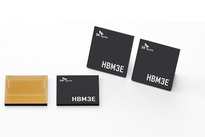
Demand for high-performance processors for AI training is skyrocketing, and consequently so is the demand for the components that go into these processors. So much so that SK hynix this week is very publicly announcing that the company's high-bandwidth memory (HBM) production capacity has already sold out for the rest of 2024, and even most of 2025 has already sold out as well.
SK hynix currently produces various types of HBM memory for customers like Amazon, AMD, Facebook, Google (Broadcom), Intel, Microsoft, and, of course, NVIDIA. The latter is an especially prolific consumer of HBM3 and HBM3E memory for its H100/H200/GH200 accelerators, as NVIDIA is also working to fill what remains an insatiable (and unmet) demand for its accelerators.
As a result, HBM memory orders, which are already placed months in advance, are now backlogging well into 2025 as chip vendors look to secure supplies of the memory stacks critical to their success.
This has made SK hynix the secnd HBM memory vendor in recent months to announce that they've sold out into 2025, following an earlier announcement from Micron regarding its HBM3E production. But of the two announcements, SK hynix's is arguably the most significant yet, as the South Korean firm's HBM production capacity is far greater than Micron's. So while things were merely "interesting" with the smallest of the Big Three memory manufacturers being sold out into 2025, things are taking a more concerning (and constrained) outlook now that SK hynix is as well.
SK hynix currently controls roughly 46% - 49% of HBM market, and its share is not expected to drop significantly in 2025, according to market tracking firm TrendForce. By contrast, Micron's share on HBM memory market is between 4% and 6%. Since HBM supply of both companies is sold out through the most of 2025, we're likely looking at a scenario where over 50% of the industry's total HBM3/HBM3E supply for the coming quarters is already sold out.
This leaves Samsung as the only member of the group not to comment on HBM demand so far. Though with memory being a highly fungible commodity product, it would be surprising if Samsung wasn't facing similar demand. And, ultimately, all of this is pointing towards the indusry entering an HBM3 memory shortage.
Separately, SK hynix said that it is sampling 12-Hi 36GB HBM3E stacks with customers and will begin volume shipments in the third quarter.
Memory

This week Samsung Electronics and Synopsys announced that Samsung has taped out its first mobile system-on-chip on Samsung Foundry's 3nm gate-all-around (GAA) process technology. The announcement, coming from electronic design automation Synopsys, further notes that Samsung used the Synopsys.ai EDA suite to place-n-route the layout and verify design of the SoC, which in turn enabled higher performance.
Samsung's unnamed high-performance mobile SoC relies on 'flagship' general-purpose CPU and GPU architectures as well as various IP blocks from Synopsys. SoC designers used Synopsys.ai EDA software, including the Synopsys DSO.ai to fine-tune design and maximize yields as well as Synopsys Fusion Compiler RTL-to-GDSII solution to achieve higher performance, lower power, and optimize area (PPA).
And while the news that Samsung has developed a high-performance SoC using the Synopsys.ai suite is important, there is another, even more important dimension to this announcement: this means that Samsung has finally taped out an advanced smartphone application processor on its cutting-edge 3nm GAAFET process.
Although Samsung Foundry has been producing chips on its GAA-equipped SF3E (3 nm-class, 'early' node) process for almost two years now, Samsung Electronics has never used this technology for its own system-on-chips for smartphones or other complex devices. To date, SF3E has been used mainly for cryptocurrency mining chips, presumably due to the inevitable early teething and yield issues that come with being the industry's first commercial GAAFET process.
For now, Samsung isn't disclosing what specific process node is being used for the SoC; the official Samsung/Synposys announcement only notes that it's for a GAA process node. Along with their first-generation 3nm-class SF3E, Samsung Foundry has a considerably more sophisticated SF3 manufacturing technology that offers numerous improvements over SF3E, and is due to be used for mass production in the coming quarters. Given the timing of the announcement, the reasonable bet is that they're using SF3.
As for Samsung's tooling partnership with Synopsys, the latter's tools are being credited for delivering some significant performance improvements to the chip's design. In particular, the two firms are crediting those tools for improving the chip's peak clockspeed by 300MHz while cutting down on dynamic power usage by 10%. To accomplish that, Samsung Electronics' SoC developers used design partitioning optimization, multi-source clock tree synthesis (MSCTS), and smart wire optimization to reduce signal interference, along with a simpler hierarchical approach. And by using Synopsys Fusion Compiler, they did all this while being able to skip weeks of 'manual' design work, according to the joint press release.
"Our longstanding collaboration has delivered leading-edge SoC designs," said Kijoon Hong, vice president of SLSI at Samsung Electronics. "This is a remarkable milestone to successfully achieve the highest performance, power and area on the most advanced mobile CPU cores and SoC designs in collaboration with Synopsys. Not only have we demonstrated that AI-driven solutions can help us achieve PPA targets for even the most advanced GAA process technologies, but through our partnership we have established an ultra-high-productivity design system that is consistently delivering impressive results."
Semiconductors
As announced last week by TSMC, later this year the company is set to start high-volume manufacturing on its N3P fabrication process, and this will be the company's most advanced node for a while. Next year things will get a bit more interesting as TSMC will have two process technologies that could actually compete against each other when they enter high-volume manufacturing (HVM) in the second half of 2025.
| Advertised PPA Improvements of New Process Technologies Data announced during conference calls, events, press briefings and press releases |
|||||||||
| Compiled by AnandTech |
TSMC | ||||||||
| N3 vs N5 |
N3E vs N5 |
N3P vs N3E |
N3X vs N3P |
N2 vs N3E |
N2P vs N3E |
N2P vs N2 |
A16 vs N2P |
||
| Power | -25% -30% |
-34% | -5% -10% |
-7%*** | -25% -30% |
-30% -40% |
-5% -10% |
-15% -20% |
|
| Performance | +10% +15% |
+18% | +5% | +5% Fmax @1.2V** |
+10% +15% |
+15% +20% |
+5 +10% |
+8% +10% |
|
| Density* | ? | 1.3x | 1.04x | 1.10x*** | 1.15x | 1.15x | ? | 1.07x 1.10x |
|
| HVM | Q4 2022 |
Q4 2023 |
H2 2024 |
H2 2025 |
H2 2025 |
H2 2026 |
H2 2026 |
H2 2026 |
|
*Chip density published by TSMC reflects 'mixed' chip density consisting of 50% logic, 30% SRAM, and 20% analog.
**At the same area.
***At the same speed.
The production nodes are N3X (3nm-class, extreme performance-focused) as well as N2 (2nm-class). TSMC says that when compared to N3P, chips made on N3X can either lower power consumption by 7% at the same frequency by lowering Vdd from 1.0V to 0.9V, increase performance by 5% at the same area, or increase transistor density by around 10% at the same frequency. Meanwhile, the key advantage of N3X compared to predecessors is its maximum voltage of 1.2V, which is important for ultra-high-performance applications, such as desktop or datacenter GPUs.
TSMC's N2 will be TSMC's first production node to use gate-all-around (GAA) nanosheet transistors and this will significantly enhance its performance, power, and are... Semiconductors
Further to our last piece which we detailed Intel's issue to motherboard vendors to follow with stock power settings for Intel's 14th and 13th Gen Core series processors, Intel has now issued a follow-up statement to this. Over the last week or so, motherboard vendors quickly released firmware updates with a new profile called 'Intel Baseline', which motherboard vendors assumed would address the instability issues.
As it turns out, Intel doesn't seem to accept this as technically, these Intel Baseline profiles are not to be confused with Intel's default specifications. This means that Intel's Baseline profiles seemingly give the impression that they are operating at default settings, hence the terminology 'baseline' used, but this still opens motherboard vendors to use their interpretations of MCE or Multi-Core Enhancement.
To clarify things for consumers, Intel has sent us the following statement:
Several motherboard manufacturers have released BIOS profiles labeled ‘Intel Baseline Profile’. However, these BIOS profiles are not the same as the 'Intel Default Settings' recommendations that Intel has recently shared with its partners regarding the instability issues reported on 13th and 14th gen K SKU processors.
These ‘Intel Baseline Profile’ BIOS settings appear to be based on power delivery guidance previously provided by Intel to manufacturers describing the various power delivery options for 13th and 14th Generation K SKU processors based on motherboard capabilities.
Intel is not recommending motherboard manufacturers to use ‘baseline’ power delivery settings on boards capable of higher values.
Intel’s recommended ‘Intel Default Settings’ are a combination of thermal and power delivery features along with a selection of possible power delivery profiles based on motherboard capabilities.
Intel recommends customers to implement the highest power delivery profile compatible with each individual motherboard design as noted in the table below:
Click to Enlarge Intel's Default Settings
What Intel's statement is effectively saying to consumers, is that users shouldn't be using the Baseline Power Delivery profiles which are offered by motherboard vendors through a plethora of firmware updates. Instead, Intel is recommending users opt for Intel Default Settings, which follows what the specific processor is rated for by Intel out of the box to achieve the clock speeds advertised, without users having to worry about firmware 'over' optimization which can cause instability as there have been many reports of happening.
Not only this, but the Intel Default settings offer a combination of thermal specifications and power capabilities, including voltage and frequency curve settings that apply to the capability of the motherboard used, and the power delivery equipped on the motherboard. At least for the most part, Intel is recommending users with 14th and 13th-Gen Core series K, KF, and KS SKUs that they do not recommend users opt in using the Baseline profiles offered by motherboard vendors.
Digesting the contrast between the two statements, the key differential is that Intel's priority is reducing the current going through the processor, which for both the 14th and 13th Gen Core series processors is a maximum of 400 A, even when using the Extreme profile. We know those motherboard vendors on their Z790 and Z690 motherboards opt for an unrestricted power profile, which is essentially 'unlimited' power and current to maximize performance at the cost of power consumption and heat, which does exacerbate problems and can lead to frequent bouts of instability, especially on high-intensity workloads.
Another variable Intel is recommending is that the AC Load Line must match the design target of the processor, with a maximum value of 1.1 mOhm, and that the DC Load Line must be ... CPUs
To say that the global foundry market is booming right now would be an understatement. Demand for leading-edge process technologies driven by AI and HPC applications is unprecedented, and with Intel joining the contract chipmaking game, this market segment is once again becoming rather competitive as well. Yet, this is exactly the market segment that Rapidus, a foundry startup backed by the Japanese government and several major Japanese companies, is going to enter in 2027, when its first fab comes online, just a few years from now.
In a fresh update on the status of bringing up the company's first leading-edge fab, Rapidus has revealed that they are intending to get in to the chip packaging game as well. Once complete, the ¥5 trillion ($32 billion) fab will be offering both chip lithography on a 2nm node, as well as packaging services for chips produced within the facility – a notable distinction in an industry where, even if packaging isn't outsourced entirely (OSAT), it's still normally handled at dedicated facilities.
Ultimately, while the company wants to serve the same clients as TSMC, Samsung, and Intel Foundry, the firm plans to do things almost completely differently than its competitors in a bid to speed up chipmaking from finishing design to getting a working chip out of the fab.
"We are very proud of being Japanese," said Henri Richard, general manager and president of Rapidus's subsidiary in the U.S. "[…] I know that some people may be looking at this thinking [that] Japan is known for quality, attention to detail, but not necessarily for speed, or flexibility. But I will tell you that Atsuyoshi Koike (the head of Rapidus) is a very special executive. That is, he has all the quality of Japan, with a lot of American thinking. So he is quite a unique guy, and certainly extraordinarily focused on creating a company that will be extremely flexible and extremely quick on its feet."
Perhaps the most significant difference between Rapidus and traditional foundries is that the company will offer only leading-edge manufacturing technologies to its clients: 2 nm in 2027 (phase 1) and then 1.4 nm in the future (phase 2). This is a stark contrast with other contract fabs, including Intel, which tend to offer their customers a full range of fabrication processes to land more clients and produce more chips. Apparently, Rapidus hopes that that there will be enough Japanese and American chip developers that are inclined to use its 2 nm fabrication process to produce their designs. With that said, the number of chip designers that are using the most advanced production node at any given time is relatively small – limited to large firms who need first-mover advantage and have the margins to justify taking the risk – so it remains to be seen whether Rapidus's business model becomes successful. The company believes it will, since the market of chips made on advanced nodes is growing rapidly.
"Until recently IDC was giving a an estimation of the 2nm and below market as about $80 billion and I think we are going to see soon a revision of the potential to $150 billion," said Richard. "[…] TSMC is the 800 pound gorilla in the space. Samsung is there and Intel is going to enter that space. But the market growth is so significant and the demand is so high, that it does not take a lot of market share for Rapidus to be successful. One of the things that gives me great comfort is that when I talk to our EDA partners, when I talk to our potential clients, it is obvious that the entire industry is looking for alternative supply from a fully independent foundry. There is a place for Samsung in this industry, there is a place for Intel in this industry, the industry is currently owned by TSMC. But another totally independent foundry is more than welcome by all of the ecosystem partners and by the customers. So, I feel really, really good about Rapidus's positioning."
Speaking of advanced process technologies, it is notable that Rapidus does not plan to use ASML's High-NA Twinscan EXE lithography scanners for 2 nm production. Instead, Rapidus is sticking to ASML's proven Low-NA scanners, which will reduce costs of Rapidus's fab, though it will entail usage of EUV double patterning, which brings up costs and lengthens the production cycle in other ways. Even with those trade-offs, SemiAnalysis analysts believe that given the cost of High-NA EUV litho tools and halved imaging field, ... Semiconductors
Further to our last piece which we detailed Intel's issue to motherboard vendors to follow with stock power settings for Intel's 14th and 13th Gen Core series processors, Intel has now issued a follow-up statement to this. Over the last week or so, motherboard vendors quickly released firmware updates with a new profile called 'Intel Baseline', which motherboard vendors assumed would address the instability issues.
As it turns out, Intel doesn't seem to accept this as technically, these Intel Baseline profiles are not to be confused with Intel's default specifications. This means that Intel's Baseline profiles seemingly give the impression that they are operating at default settings, hence the terminology 'baseline' used, but this still opens motherboard vendors to use their interpretations of MCE or Multi-Core Enhancement.
To clarify things for consumers, Intel has sent us the following statement:
Several motherboard manufacturers have released BIOS profiles labeled ‘Intel Baseline Profile’. However, these BIOS profiles are not the same as the 'Intel Default Settings' recommendations that Intel has recently shared with its partners regarding the instability issues reported on 13th and 14th gen K SKU processors.
These ‘Intel Baseline Profile’ BIOS settings appear to be based on power delivery guidance previously provided by Intel to manufacturers describing the various power delivery options for 13th and 14th Generation K SKU processors based on motherboard capabilities.
Intel is not recommending motherboard manufacturers to use ‘baseline’ power delivery settings on boards capable of higher values.
Intel’s recommended ‘Intel Default Settings’ are a combination of thermal and power delivery features along with a selection of possible power delivery profiles based on motherboard capabilities.
Intel recommends customers to implement the highest power delivery profile compatible with each individual motherboard design as noted in the table below:
Click to Enlarge Intel's Default Settings
What Intel's statement is effectively saying to consumers, is that users shouldn't be using the Baseline Power Delivery profiles which are offered by motherboard vendors through a plethora of firmware updates. Instead, Intel is recommending users opt for Intel Default Settings, which follows what the specific processor is rated for by Intel out of the box to achieve the clock speeds advertised, without users having to worry about firmware 'over' optimization which can cause instability as there have been many reports of happening.
Not only this, but the Intel Default settings offer a combination of thermal specifications and power capabilities, including voltage and frequency curve settings that apply to the capability of the motherboard used, and the power delivery equipped on the motherboard. At least for the most part, Intel is recommending users with 14th and 13th-Gen Core series K, KF, and KS SKUs that they do not recommend users opt in using the Baseline profiles offered by motherboard vendors.
Digesting the contrast between the two statements, the key differential is that Intel's priority is reducing the current going through the processor, which for both the 14th and 13th Gen Core series processors is a maximum of 400 A, even when using the Extreme profile. We know those motherboard vendors on their Z790 and Z690 motherboards opt for an unrestricted power profile, which is essentially 'unlimited' power and current to maximize performance at the cost of power consumption and heat, which does exacerbate problems and can lead to frequent bouts of instability, especially on high-intensity workloads.
Another variable Intel is recommending is that the AC Load Line must match the design target of the processor, with a maximum value of 1.1 mOhm, and that the DC Load Line must be ... CPUs
As LPCAMM2 adoption begins, the first retail memory modules are finally starting to hit the retail market, courtesy of Micron. The memory manufacturer has begun selling their LPDDR5X-based LPCAMM2 memory modules under their in-house Crucial brand, making them available on the latter's storefront. Timed to coincide with the release of Lenovo's ThinkPad P1 Gen 7 laptop – the first retail laptop designed to use the memory modules – this marks the de facto start of the eagerly-awaited modular LPDDR5X memory era.
Micron's Low Power Compression Attached Memory Module 2 (LPCAMM2) modules are available in capacities of 32 GB and 64 GB. These are dual-channel modules that feature a 128-bit wide interface, and are based around LPDDR5X memory running at data rates up to 7500 MT/s. This gives a single LPCAMM2 a peak bandwidth of 120 GB/s. Micron is not disclosing the latencies of its LPCAMM2 memory modules, but it says that high data transfer rates of LPDDR5X compensate for the extended timings.
Micron says that LPDDR5X memory offers significantly lower power consumption, with active power per 64-bit bus being 43-58% lower than DDR5 at the same speed, and standby power up to 80% lower. Meanwhile, similar to DDR5 modules, LPCAMM2 modules include a power management IC and voltage regulating circuitry, which provides module manufacturers additional opportunities to reduce power consumption of their products.
Source: Micron LPDDR5X LPCAMM2 Technical Brief
It's worth noting, however, that at least for the first generation of LPCAMM2 modules, system vendors will need to pick between modularity and performance. While soldered-down LPDDR5X memory is available at speeds up to 8533 MT/sec – and with 9600 MT/sec on the horizon – the fastest LPCAMM2 modules planned for this year by both Micron and rival Samsung will be running at 7500 MT/sec. So vendors will have to choose between the flexibility of offering modular LPDDR5X, or the higher bandwidth (and space savings) offered by soldering down their memory.
Micron, for its part, is projecting that 9600 MT/sec LPCAMM2 modules will be available by 2026. Though it's all but certain that faster memory will also be avaialble in the same timeframe.
Micron's Crucial LPDDR5X 32 GB module costs $174.99, whereas a 64 GB module costs $329.99.
Memory
Demand for high-performance processors for AI training is skyrocketing, and consequently so is the demand for the components that go into these processors. So much so that SK hynix this week is very publicly announcing that the company's high-bandwidth memory (HBM) production capacity has already sold out for the rest of 2024, and even most of 2025 has already sold out as well.
SK hynix currently produces various types of HBM memory for customers like Amazon, AMD, Facebook, Google (Broadcom), Intel, Microsoft, and, of course, NVIDIA. The latter is an especially prolific consumer of HBM3 and HBM3E memory for its H100/H200/GH200 accelerators, as NVIDIA is also working to fill what remains an insatiable (and unmet) demand for its accelerators.
As a result, HBM memory orders, which are already placed months in advance, are now backlogging well into 2025 as chip vendors look to secure supplies of the memory stacks critical to their success.
This has made SK hynix the secnd HBM memory vendor in recent months to announce that they've sold out into 2025, following an earlier announcement from Micron regarding its HBM3E production. But of the two announcements, SK hynix's is arguably the most significant yet, as the South Korean firm's HBM production capacity is far greater than Micron's. So while things were merely "interesting" with the smallest of the Big Three memory manufacturers being sold out into 2025, things are taking a more concerning (and constrained) outlook now that SK hynix is as well.
SK hynix currently controls roughly 46% - 49% of HBM market, and its share is not expected to drop significantly in 2025, according to market tracking firm TrendForce. By contrast, Micron's share on HBM memory market is between 4% and 6%. Since HBM supply of both companies is sold out through the most of 2025, we're likely looking at a scenario where over 50% of the industry's total HBM3/HBM3E supply for the coming quarters is already sold out.
This leaves Samsung as the only member of the group not to comment on HBM demand so far. Though with memory being a highly fungible commodity product, it would be surprising if Samsung wasn't facing similar demand. And, ultimately, all of this is pointing towards the indusry entering an HBM3 memory shortage.
Separately, SK hynix said that it is sampling 12-Hi 36GB HBM3E stacks with customers and will begin volume shipments in the third quarter.
Memory
Demand for high-performance processors for AI training is skyrocketing, and consequently so is the demand for the components that go into these processors. So much so that SK hynix this week is very publicly announcing that the company's high-bandwidth memory (HBM) production capacity has already sold out for the rest of 2024, and even most of 2025 has already sold out as well.
SK hynix currently produces various types of HBM memory for customers like Amazon, AMD, Facebook, Google (Broadcom), Intel, Microsoft, and, of course, NVIDIA. The latter is an especially prolific consumer of HBM3 and HBM3E memory for its H100/H200/GH200 accelerators, as NVIDIA is also working to fill what remains an insatiable (and unmet) demand for its accelerators.
As a result, HBM memory orders, which are already placed months in advance, are now backlogging well into 2025 as chip vendors look to secure supplies of the memory stacks critical to their success.
This has made SK hynix the secnd HBM memory vendor in recent months to announce that they've sold out into 2025, following an earlier announcement from Micron regarding its HBM3E production. But of the two announcements, SK hynix's is arguably the most significant yet, as the South Korean firm's HBM production capacity is far greater than Micron's. So while things were merely "interesting" with the smallest of the Big Three memory manufacturers being sold out into 2025, things are taking a more concerning (and constrained) outlook now that SK hynix is as well.
SK hynix currently controls roughly 46% - 49% of HBM market, and its share is not expected to drop significantly in 2025, according to market tracking firm TrendForce. By contrast, Micron's share on HBM memory market is between 4% and 6%. Since HBM supply of both companies is sold out through the most of 2025, we're likely looking at a scenario where over 50% of the industry's total HBM3/HBM3E supply for the coming quarters is already sold out.
This leaves Samsung as the only member of the group not to comment on HBM demand so far. Though with memory being a highly fungible commodity product, it would be surprising if Samsung wasn't facing similar demand. And, ultimately, all of this is pointing towards the indusry entering an HBM3 memory shortage.
Separately, SK hynix said that it is sampling 12-Hi 36GB HBM3E stacks with customers and will begin volume shipments in the third quarter.
Memory
As announced last week by TSMC, later this year the company is set to start high-volume manufacturing on its N3P fabrication process, and this will be the company's most advanced node for a while. Next year things will get a bit more interesting as TSMC will have two process technologies that could actually compete against each other when they enter high-volume manufacturing (HVM) in the second half of 2025.
| Advertised PPA Improvements of New Process Technologies Data announced during conference calls, events, press briefings and press releases |
|||||||||
| Compiled by AnandTech |
TSMC | ||||||||
| N3 vs N5 |
N3E vs N5 |
N3P vs N3E |
N3X vs N3P |
N2 vs N3E |
N2P vs N3E |
N2P vs N2 |
A16 vs N2P |
||
| Power | -25% -30% |
-34% | -5% -10% |
-7%*** | -25% -30% |
-30% -40% |
-5% -10% |
-15% -20% |
|
| Performance | +10% +15% |
+18% | +5% | +5% Fmax @1.2V** |
+10% +15% |
+15% +20% |
+5 +10% |
+8% +10% |
|
| Density* | ? | 1.3x | 1.04x | 1.10x*** | 1.15x | 1.15x | ? | 1.07x 1.10x |
|
| HVM | Q4 2022 |
Q4 2023 |
H2 2024 |
H2 2025 |
H2 2025 |
H2 2026 |
H2 2026 |
H2 2026 |
|
*Chip density published by TSMC reflects 'mixed' chip density consisting of 50% logic, 30% SRAM, and 20% analog.
**At the same area.
***At the same speed.
The production nodes are N3X (3nm-class, extreme performance-focused) as well as N2 (2nm-class). TSMC says that when compared to N3P, chips made on N3X can either lower power consumption by 7% at the same frequency by lowering Vdd from 1.0V to 0.9V, increase performance by 5% at the same area, or increase transistor density by around 10% at the same frequency. Meanwhile, the key advantage of N3X compared to predecessors is its maximum voltage of 1.2V, which is important for ultra-high-performance applications, such as desktop or datacenter GPUs.
TSMC's N2 will be TSMC's first production node to use gate-all-around (GAA) nanosheet transistors and this will significantly enhance its performance, power, and are... Semiconductors

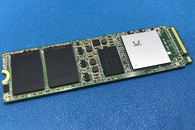
While Realtek is best known in the enthusiast space for for its peripheral controllers such as audio codecs and network controllers, the company also has a small-but-respectable SSD controller business that tends to fly under the radar due to its focus on entry-level and mainstream drives. But Realtek's stature in the SSD space is on the rise, as the company is not only planning new PCIe Gen5 SSD controllers, but also their first high-end, DRAM-equipped SSD controller.
For this year's Computex trade show, Realtek laid out a new SSD controller roadmap that calls for the company to release a trio of new SSD controllers over the next couple of years. First up is a new four-channel entry-level PCIe 4.0 controller, the RTS5776DL, which will be joined a bit later by a PCIe 5.0 variant, the RTS5781DL. But most interesting on Realtek's new roadmap is the final chip being planned: the eight-channel, DRAM-equipped RTS5782, which would be the company's first high-end SSD controller, capable of hitting sequential read rates as high as 14GB/second.
| Realtek NVMe SSD Controller Comparison | |||||||||
| RTS5782 | RTS5781DL | RTS5776DL | RTS5772DL | RTS5766DL | |||||
| Market Segment | High-End | Mainstream | Entry-Level | ||||||
| Error Correction | 4K LDPC | 2K LDPC | |||||||
| DRAM | DDR4, LPDDR4(X) | No | No | No | No | ||||
| Host Interface | PCIe 5.0 x4 | PCIe 5.0 x4 | PCIe 4.0 x4 | PCIe 4.0 x4 | PCIe 3.0 x4 | ||||
| NVMe Version | NVMe 2.0 | NVMe 2.0 | NVMe 2.0 | NVMe 1.4 | NVMe 1.4 | ||||
| NAND Channels, Interface Speed | 8 ch, 3600 MT/s |
4 ch, 3600 MT/s |
4 ch, 3600 MT/s |
8 ch, 1600 MT/s |
4 ch, 1200 MT/s |
||||
| Sequential Read | 14 GB/s | 10 GB/s | 7.4 GB/s | 6 GB/s | 3.2 GB/s | ||||
| Sequential Write | 12 GB/s | 10 GB/s | 7.4 GB/s | 6 GB/s | 2.2 GB/s | ||||
| 4KB Random Read IOPS | 2500k | 1400k | 1200k | - | - | ||||
| 4KB Random Write IOPS | 2500k | 1400k | 1200k | - | - | ||||
Diving a bit deeper into Realtek's roadmap, the RTS5776DL is traditional DRAM-less PCIe Gen4 x4 controller with four NAND chann... SSDs

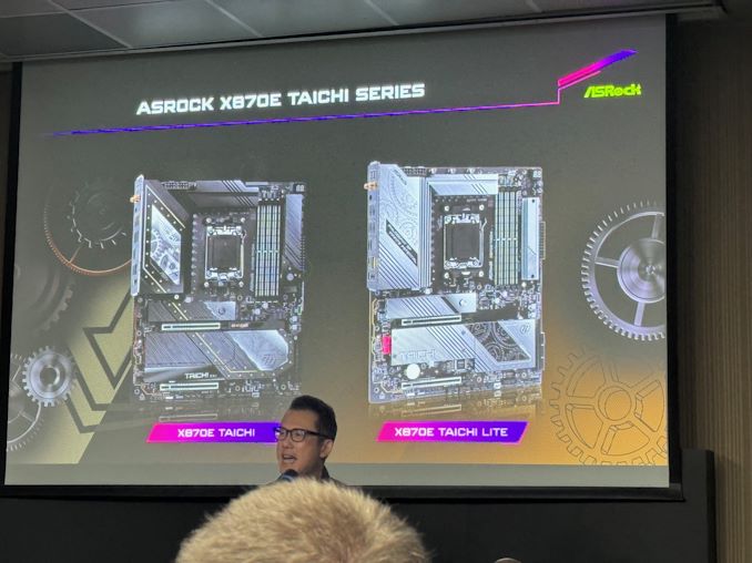
During Computex 2024, ASRock held an event to unveil some of its upcoming X870E motherboards, designed for AMD's Zen 5-based Ryzen 9000 series processors. ASRock's announcement includes a pair of Taichi-branded boards, the X870E Taichi and the lighter X870E Taichi lite, which uses AMD's X870E (Promontory 21) chipset for AM5.
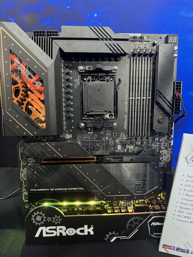
The current flagship model announced from ASRock's X870E line-up for Ryzen 9000 is the ASRock X870E Taichi. ASRock is advertising a large 27-phase power delivery through 110A SPS, suggesting this board is designed for overclockers and all-around power users. Two PCIe 5.0 x16 slots (operating in either x16/x0 or x8/x8) provide high-speed bandwidth for cutting-edge graphics cards and other devices. Meanwhile, ASRock has gone with 4 DIMM slots on this board, so system builders will be able to max out the board's memory capacity at the cost of bandwidth.
The storage offering is impressive; besides the obligatory PCIe Gen5 x4 M.2 slot (Blazing M.2), ASRock has outfit the board with another three PCIe Gen4 x4 (Hyper) M.2 slots. Also present are two USB4 Type-C ports for high-bandwidth external I/O, while networking support is a solid pairing of a discrete Wi-Fi 7 controller with a Realtek 5Gb Ethernet controller (and the first AM5 board we've come across with something faster than a 2.5GbE controller).
The audio setup includes a Realtek ALC4082 codec and ESS SABRE9218 DAC supporting high-fidelity sound. The BIOS flashback feature is also a nice touch, and we believe this should be a feature on all mid-range to high-end motherboards, which provides an easy way to update the firmware without installing a CPU. And, as no high-end board would be complete without it, ASRock has put RGB lighting on the X870E Taichi as well.
Ultimately, as ASRock's high-end X870E board, the X870E Taichi comes with pretty much every last cutting-edge technology that ASRock can fit on the board.
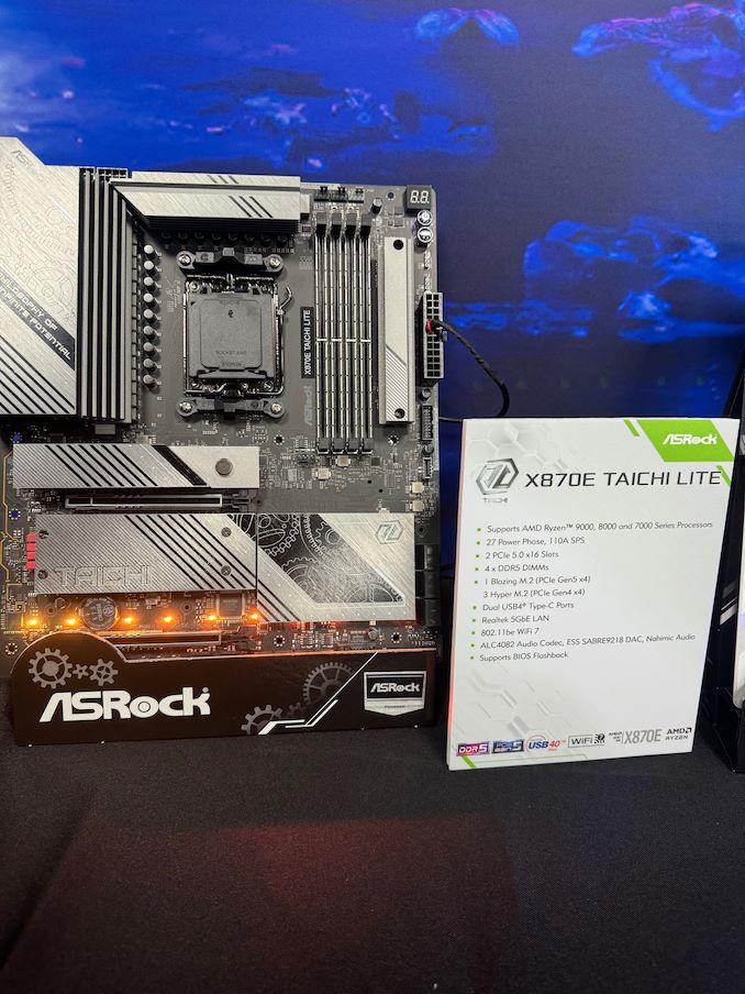
Comparatively, the ASRock X870E Taichi Lite is a more streamlined and functional version of the X870E Taichi. The Lite retaining all of the latter's key features, including the 27-phase power delivery with 110A smart power stages, dual PCIe 5.0 x16 slots operating at x16 or x8/x8, four DDR5 DIMM slots, and four M.2 slots (1x Gen5 + 3x Gen4). The only significant difference is aesthetics: the Taichi Lite features a simpler silver-themed design without the RGB lighting, while the standard Taichi has a more intricate gold-accented and fanciful aesthetics.
In terms of availability, ASRock is not disclosing a release date for the board at the show. And, checking around with other tech journalists, Andreas Schilling from HawrdwareLUXX has heard that X870E and X870 motherboards aren't expected to be available in time for the Ryzen 9000 series launch. We will investigate this and contact the motherboard vendors to confirm the situation. Though as X870E/X870 boards barely differ from the current crop of X670E/B650E boards to begin with, the Ryzen 9000 series won't be fazed by a lack of slightly newer motherboards.
Motherboards
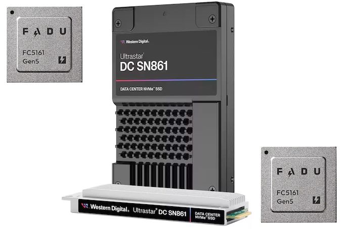
When Western Digital introduced its Ultrastar DC SN861 SSDs earlier this year, the company did not disclose which controller it used for these drives, which made many observers presume that WD was using an in-house controller. But a recent teardown of the drive shows that is not the case; instead, the company is using a controller from Fadu, a South Korean company founded in 2015 that specializes on enterprise-grade turnkey SSD solutions.
The Western Digital Ultrastar DC SN861 SSD is aimed at performance-hungry hyperscale datacenters and enterprise customers which are adopting PCIe Gen5 storage devices these days. And, as uncovered in photos from a recent Storage Review article, the drive is based on Fadu's FC5161 NVMe 2.0-compliant controller. The FC5161 utilizes 16 NAND channels supporting an ONFi 5.0 2400 MT/s interface, and features a combination of enterprise-grade capabilities (OCP Cloud Spec 2.0, SR-IOV, up to 512 name spaces for ZNS support, flexible data placement, NVMe-MI 1.2, advanced security, telemetry, power loss protection) not available on other off-the-shelf controllers – or on any previous Western Digital controllers.
The Ultrastar DC SN861 SSD offers sequential read speeds up to 13.7 GB/s as well as sequential write speeds up to 7.5 GB/s. As for random performance, it boasts with an up to 3.3 million random 4K read IOPS and up to 0.8 million random 4K write IOPS. The drives are available in capacities between 1.6 TB and 7.68 TB with one or three drive writes per day (DWPD) over five years rating as well as in U.2 and E1.S form-factors.
While the two form factors of the SN861 share a similar technical design, Western Digital has tailored each version for distinct workloads: the E1.S supports FDP and performance enhancements specifically for cloud environments. By contrast, the U.2 model is geared towards high-performance enterprise tasks and emerging applications like AI.
Without any doubts, Western Digital's Ultrastar DC SN861 is a feature-rich high-performance enterprise-grade SSD. It has another distinctive feature: a 5W idle power consumption, which is rather low by the standards of enterprise-grade drives (e.g., it is 1W lower compared to the SN840). While the difference with predecessors may be just 1W, hyperscalers deploy thousands of drives and for their TCO every watt counts.
Western Digital's Ultrastar DC SN861 SSDs are now available for purchase to select customers (such as Meta) and to interested parties. Prices are unknown, but they will depend on such factors as volumes.
Sources: Fadu, Storage Review
Storage
While Realtek is best known in the enthusiast space for for its peripheral controllers such as audio codecs and network controllers, the company also has a small-but-respectable SSD controller business that tends to fly under the radar due to its focus on entry-level and mainstream drives. But Realtek's stature in the SSD space is on the rise, as the company is not only planning new PCIe Gen5 SSD controllers, but also their first high-end, DRAM-equipped SSD controller.
For this year's Computex trade show, Realtek laid out a new SSD controller roadmap that calls for the company to release a trio of new SSD controllers over the next couple of years. First up is a new four-channel entry-level PCIe 4.0 controller, the RTS5776DL, which will be joined a bit later by a PCIe 5.0 variant, the RTS5781DL. But most interesting on Realtek's new roadmap is the final chip being planned: the eight-channel, DRAM-equipped RTS5782, which would be the company's first high-end SSD controller, capable of hitting sequential read rates as high as 14GB/second.
| Realtek NVMe SSD Controller Comparison | |||||||||
| RTS5782 | RTS5781DL | RTS5776DL | RTS5772DL | RTS5766DL | |||||
| Market Segment | High-End | Mainstream | Entry-Level | ||||||
| Error Correction | 4K LDPC | 2K LDPC | |||||||
| DRAM | DDR4, LPDDR4(X) | No | No | No | No | ||||
| Host Interface | PCIe 5.0 x4 | PCIe 5.0 x4 | PCIe 4.0 x4 | PCIe 4.0 x4 | PCIe 3.0 x4 | ||||
| NVMe Version | NVMe 2.0 | NVMe 2.0 | NVMe 2.0 | NVMe 1.4 | NVMe 1.4 | ||||
| NAND Channels, Interface Speed | 8 ch, 3600 MT/s |
4 ch, 3600 MT/s |
4 ch, 3600 MT/s |
8 ch, 1600 MT/s |
4 ch, 1200 MT/s |
||||
| Sequential Read | 14 GB/s | 10 GB/s | 7.4 GB/s | 6 GB/s | 3.2 GB/s | ||||
| Sequential Write | 12 GB/s | 10 GB/s | 7.4 GB/s | 6 GB/s | 2.2 GB/s | ||||
| 4KB Random Read IOPS | 2500k | 1400k | 1200k | - | - | ||||
| 4KB Random Write IOPS | 2500k | 1400k | 1200k | - | - | ||||
Diving a bit deeper into Realtek's roadmap, the RTS5776DL is traditional DRAM-less PCIe Gen4 x4 controller with four NAND chann... SSDs
During Computex 2024, ASRock held an event to unveil some of its upcoming X870E motherboards, designed for AMD's Zen 5-based Ryzen 9000 series processors. ASRock's announcement includes a pair of Taichi-branded boards, the X870E Taichi and the lighter X870E Taichi lite, which uses AMD's X870E (Promontory 21) chipset for AM5.
The current flagship model announced from ASRock's X870E line-up for Ryzen 9000 is the ASRock X870E Taichi. ASRock is advertising a large 27-phase power delivery through 110A SPS, suggesting this board is designed for overclockers and all-around power users. Two PCIe 5.0 x16 slots (operating in either x16/x0 or x8/x8) provide high-speed bandwidth for cutting-edge graphics cards and other devices. Meanwhile, ASRock has gone with 4 DIMM slots on this board, so system builders will be able to max out the board's memory capacity at the cost of bandwidth.
The storage offering is impressive; besides the obligatory PCIe Gen5 x4 M.2 slot (Blazing M.2), ASRock has outfit the board with another three PCIe Gen4 x4 (Hyper) M.2 slots. Also present are two USB4 Type-C ports for high-bandwidth external I/O, while networking support is a solid pairing of a discrete Wi-Fi 7 controller with a Realtek 5Gb Ethernet controller (and the first AM5 board we've come across with something faster than a 2.5GbE controller).
The audio setup includes a Realtek ALC4082 codec and ESS SABRE9218 DAC supporting high-fidelity sound. The BIOS flashback feature is also a nice touch, and we believe this should be a feature on all mid-range to high-end motherboards, which provides an easy way to update the firmware without installing a CPU. And, as no high-end board would be complete without it, ASRock has put RGB lighting on the X870E Taichi as well.
Ultimately, as ASRock's high-end X870E board, the X870E Taichi comes with pretty much every last cutting-edge technology that ASRock can fit on the board.
Comparatively, the ASRock X870E Taichi Lite is a more streamlined and functional version of the X870E Taichi. The Lite retaining all of the latter's key features, including the 27-phase power delivery with 110A smart power stages, dual PCIe 5.0 x16 slots operating at x16 or x8/x8, four DDR5 DIMM slots, and four M.2 slots (1x Gen5 + 3x Gen4). The only significant difference is aesthetics: the Taichi Lite features a simpler silver-themed design without the RGB lighting, while the standard Taichi has a more intricate gold-accented and fanciful aesthetics.
In terms of availability, ASRock is not disclosing a release date for the board at the show. And, checking around with other tech journalists, Andreas Schilling from HawrdwareLUXX has heard that X870E and X870 motherboards aren't expected to be available in time for the Ryzen 9000 series launch. We will investigate this and contact the motherboard vendors to confirm the situation. Though as X870E/X870 boards barely differ from the current crop of X670E/B650E boards to begin with, the Ryzen 9000 series won't be fazed by a lack of slightly newer motherboards.
Motherboards
When Western Digital introduced its Ultrastar DC SN861 SSDs earlier this year, the company did not disclose which controller it used for these drives, which made many observers presume that WD was using an in-house controller. But a recent teardown of the drive shows that is not the case; instead, the company is using a controller from Fadu, a South Korean company founded in 2015 that specializes on enterprise-grade turnkey SSD solutions.
The Western Digital Ultrastar DC SN861 SSD is aimed at performance-hungry hyperscale datacenters and enterprise customers which are adopting PCIe Gen5 storage devices these days. And, as uncovered in photos from a recent Storage Review article, the drive is based on Fadu's FC5161 NVMe 2.0-compliant controller. The FC5161 utilizes 16 NAND channels supporting an ONFi 5.0 2400 MT/s interface, and features a combination of enterprise-grade capabilities (OCP Cloud Spec 2.0, SR-IOV, up to 512 name spaces for ZNS support, flexible data placement, NVMe-MI 1.2, advanced security, telemetry, power loss protection) not available on other off-the-shelf controllers – or on any previous Western Digital controllers.
The Ultrastar DC SN861 SSD offers sequential read speeds up to 13.7 GB/s as well as sequential write speeds up to 7.5 GB/s. As for random performance, it boasts with an up to 3.3 million random 4K read IOPS and up to 0.8 million random 4K write IOPS. The drives are available in capacities between 1.6 TB and 7.68 TB with one or three drive writes per day (DWPD) over five years rating as well as in U.2 and E1.S form-factors.
While the two form factors of the SN861 share a similar technical design, Western Digital has tailored each version for distinct workloads: the E1.S supports FDP and performance enhancements specifically for cloud environments. By contrast, the U.2 model is geared towards high-performance enterprise tasks and emerging applications like AI.
Without any doubts, Western Digital's Ultrastar DC SN861 is a feature-rich high-performance enterprise-grade SSD. It has another distinctive feature: a 5W idle power consumption, which is rather low by the standards of enterprise-grade drives (e.g., it is 1W lower compared to the SN840). While the difference with predecessors may be just 1W, hyperscalers deploy thousands of drives and for their TCO every watt counts.
Western Digital's Ultrastar DC SN861 SSDs are now available for purchase to select customers (such as Meta) and to interested parties. Prices are unknown, but they will depend on such factors as volumes.
Sources: Fadu, Storage Review
Storage
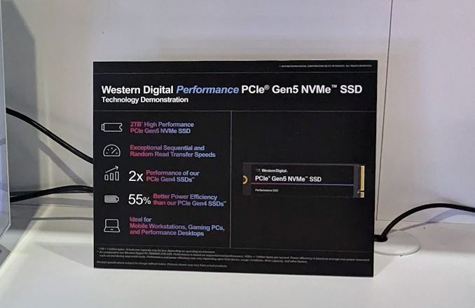
Western Digital's FMS 2024 demonstrations included a preview of their upcoming PCIe 5.0 x4 M.2 2280 NVMe SSDs for mobile workstations and consumer desktops. The Gen 5 client SSD market has been dominated by solutions based on Phison's E26 controller. The first generation products launched with slower NAND flash, while the more recent ones have exceeded the 14 GBps barrier by utilizing Micron's 2400 MT/s 232L 3D TLC. Western Digital has been conservative over the last year or so by focusing more on the mainstream / mid-range market in terms of new product introductions (such as the WD Blue SN5000, WD_BLACK SN770M, and the WD Blue SN580). Their SSD lineup is due for an update with Gen 5 drives being sorely missed. The SSDs being demonstrated at FMS 2024 will end up doing just that.
Western Digital's technology demonstrations in this segment involved two different M.2 2280 SSDs - one for the performance segment, and another for the mainstream market. They both utilize in-house controllers - while the performance segment drive uses a 8-channel controller with DRAM for the flash translation layer, the mainstream one utilizes a 4-channel DRAM-less controller. Both drives being benchmarked live were equipped with BiCS8 218-layer 3D TLC.
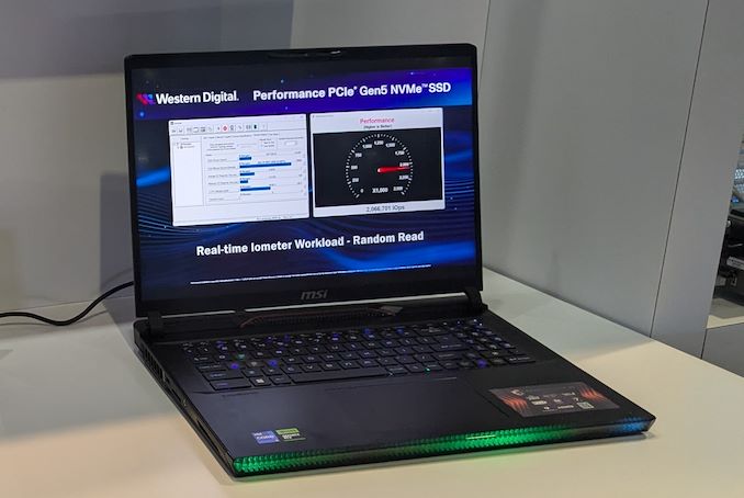
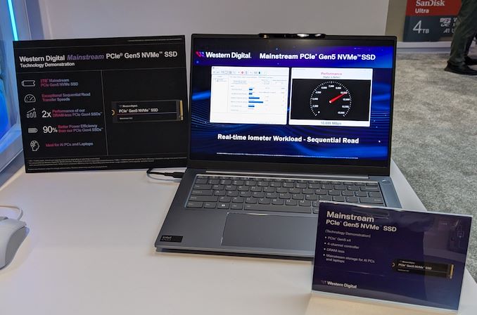
Western Digital is touting the power efficiency of their platform as a key differentiator, promising south of 7W (performance drive) and 5W (mainstream DRAM-less drive) for the complete SSD under stressful traffic. This makes it suitable for use in mobile workstations, but a good fit for desktops as well.
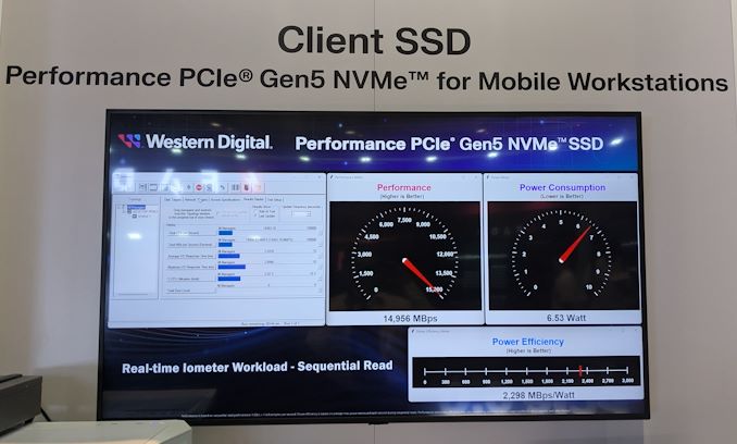
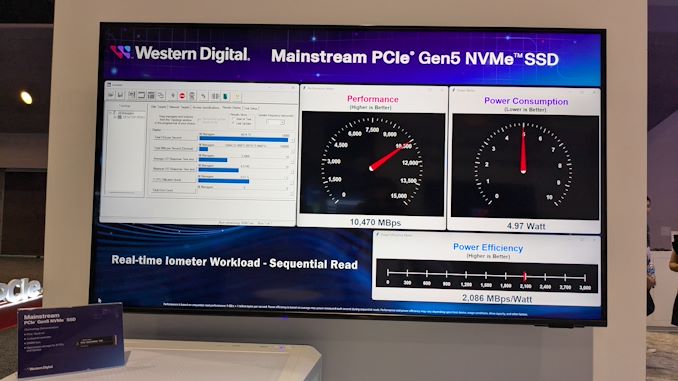
Demonstrated performance numbers indicate almost 15 GBps sequential reads and 2M+ random read IOPS for the performance drive, and 10.7 GBps sequential reads for the mainstream version. Western Digital might have missed the Gen 5 bus as it started out slowly. However, the technology demonstrations with the in-house controller and NAND indicate that WD has caught up just as the Gen 5 market is about to take off.|
Storage
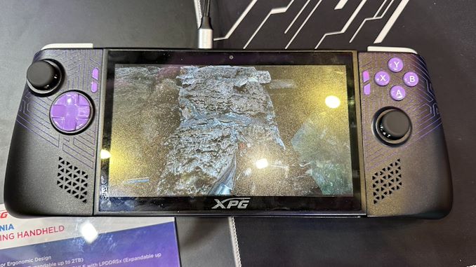
With the rise of the handheld gaming PC market, we've seen PC vendors and their partners toy with a number of tricks and tweaks to improve improve framerates in games, with some of their latest efforts on display at this year's Computex trade show. Perhaps the most interesting find thus far comes from ADATA sub-brand XPG, who is demoing their prototype "Nia" handheld PC, which uses eye tracking and dynamic foveated rendering to further improve their rendering performance.
For those unfamiliar, dynamic foveated rendering is a graphics technique that is sometimes used to boost performance in virtual reality (VR) and augmented reality (AR) applications by taking advantage of how human vision works. Typically, humans can only perceive detailed imagery in the relatively small central area of our vision called the fovea, while our peripheral vision is much less detailed. Dynamic foveated rendering, in turn, exploits this by using real-time eye tracking to determine where the user is looking, and then rendering just that area in high/full resolution, while rendering the peripheral areas in lower resolution. The net result is that only a fraction of the screen is rendered at full detail, which cuts down on the total amount of rendering work required and boosting framerates on performance-limited devices.
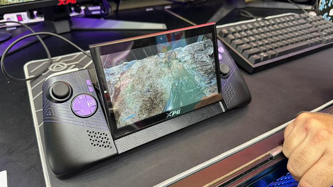
As stated before, this technology is sometimes used in high-end AR/VR headsets, where high resolution displays are placed mere inches from one's face. This ends up being an ideal use case for the technique, since at those distances, only a small fraction of the screen is within the fovea.
Using dynamic foveated rendering for a handheld, on the other hand, is a more novel application. All of the same visual principles apply, but the resolutions at play are lower, and the screen is farther from the users' eyes. This makes a handheld device a less ideal use case, at least on paper, as a larger portion of the screen is going to be in the fovea, and thus will need to be rendered at full resolution. None the less, it will be interesting to see how XPG's efforts pan out, and if dynamic foveated rendering is beneficial enough for handheld PCs. As we sometimes see with trade show demos, not everything makes it out of the prototype stage.
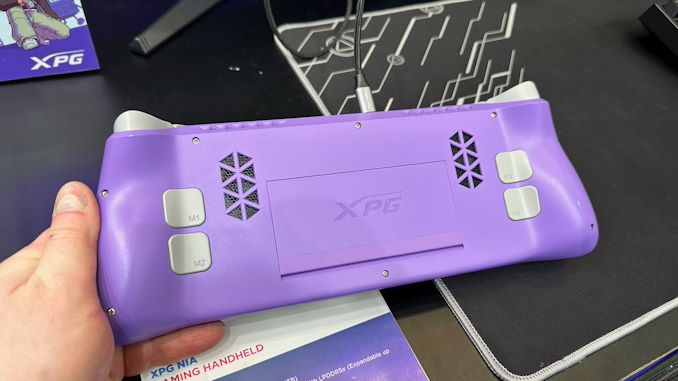
According to a press release put out by ADATA ahead of the trade show, the eye tracking technology is being provided by AMD collaborator Eyeware. Notably, their software-based approach runs on top of standard webcams, rather than requiring IR cameras. So the camera hardware itself should be pretty straight-forward.
Foveated rendering aside, XPG is making sure that the Nia won't be a one-trick pony. The handheld's other major claim to fame is its hardware swappability. The prototype handheld not only features a removable M.2-2230 SSD, but the company is also taking advantage of the recently-introduced LPCAMM2 memory module standard to introduce removable DRAM. Via a hatch in the back of the handheld, device owners would be able to swap out LPCAMM2 LPDDR5X modules for higher capacity versions. This would give the handheld an additional degree of future-proofness over current handhelds, which use non-replaceable soldered-down memory.
Rounding out the package, the current prototype is based on an AMD's Zen 4 Phoenix APU, which is used across both of the company's current mobile lines (Ryzen Mobile 7000/8000 and Ryzen Z1). Meanwhile, the unit's display is adjustable, allowing it to be angled away from the body of the handheld.
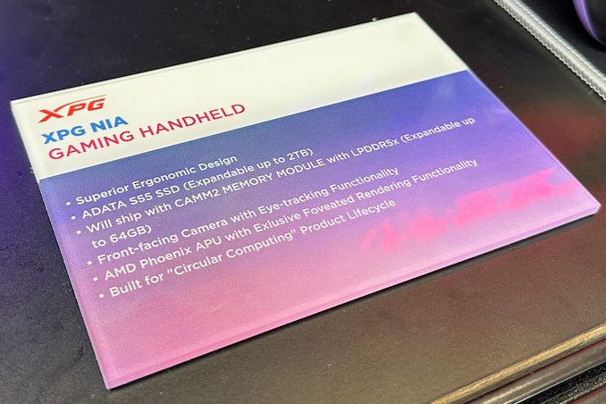
Assuming all goes well with the prototype, XPG aims to release a finished product in 2025.
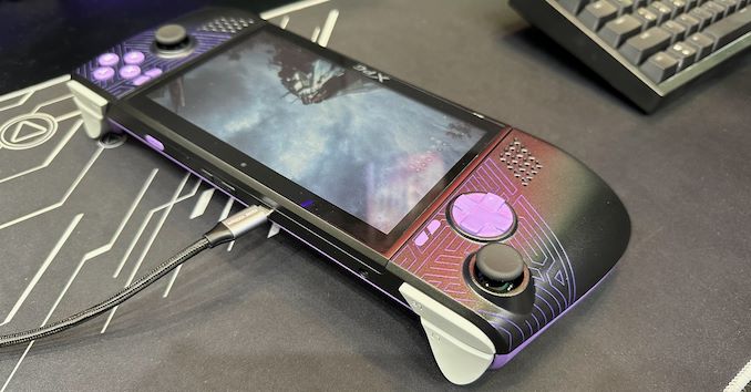
In addition to revealing its roadmap and plans concerning its current leading-edge process technologies, TSMC also shared progress of its N2 node as part of its Symposiums 2024. The company's first 2nm-class fabrication node, and predominantly featuring gate-all-around transistors, according to TSMC N2 has almost achieved its target performance and yield goals, which places it on track to enter high-volume manufacturing in the second half of 2025.
TSMC states that 'N2 development is well on track and N2P is next.' In particular, gate-all-around nanosheet devices currently achieve over 90% of their expected performance, whereas yields of 256 Mb SRAM (32 MB) devices already exceeds 80%, depending on the batch. All of this for a node that is over a year away from mass production.
Meanwhile, average yield of a 256 Mb SRAM was around 70% as of March, 2024, up from around 35% in April, 2023. Device performance has also been improving with higher frequencies being achieved while keeping power consumption in check.
Chip designer interest towards TSMC's first 2nm-class gate-all-around nanosheet transistor-based technology is significant, too. The number of new tape-outs (NTOs) in the first year of N2 is over two-times higher than it was for N5. Though with that said, given TSMC's close working relationship with a handful of high-volume vendors – most notably Appe – NTOs can be a very misleading figure since the first year of a new node at TSMC is capacity constrained, and consequently the bulk of that capacity goes to TSMC's priority partners.
Meanwhile, there were considerably more N5 tapeouts in its second year (some where N5P, of course) and N2 promises to have 2.6X more NTOs in its second year. So the node indeed looks quite promising. In fact, based on TSMC's slides (which we're unfortunately not able to republish), N2 is more popular than N3 in terms of NTOs both in the first and the second years of existence.
When it comes to the second year of N2, in the second half of 2026 TSMC plans to roll out its N2P technology, which promises additional performance and power benefits. N2P is expected to improve frequency by 15% - 20%, reduce power consumption by 30% - 40%, and increase chip density by over 1.15 times compared to N3E, significant benefits to move to all-new GAA nanosheet transistors.
Finally, for those companies that need the best in performance, power, and density, TSMC is poised to offer their A16 process in 2026. That node will also bring in backside power delivery, which will add costs, but is expected to greatly improve performance efficiency and scaling.
Semiconductors
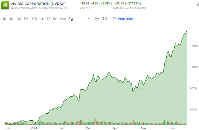
Thanks to the success of the burgeoning market for AI accelerators, NVIDIA has been on a tear this year. And the only place that’s even more apparent than the company’s rapidly growing revenues is in the company’s stock price and market capitalization. After breaking into the top 5 most valuable companies only earlier this year, NVIDIA has reached the apex of Wall Street, closing out today as the world’s most valuable company.
With a closing price of $135.58 on a day that saw NVIDIA’s stock pop up another 3.5%, NVIDIA has topped both Microsoft and Apple in valuation, reaching a market capitalization of $3.335 trillion. This follows a rapid rise in the company’s stock price, which has increased by 47% in the last month alone – particularly on the back of NVIDIA’s most recent estimates-beating earnings report – as well as a recent 10-for-1 stock split. And looking at the company’s performance over a longer time period, NVIDIA’s stock jumped a staggering 218% over the last year, or a mere 3,474% over the last 5 years.
NVIDIA’s ascension continues a trend over the last several years of tech companies all holding the top spots in the market capitalization rankings. Though this is the first time in quite a while that the traditional tech leaders of Apple and Microsoft have been pushed aside.
| Market Capitalization Rankings | ||
| Market Cap | Stock Price | |
| NVIDIA | $3.335T | $135.58 |
| Microsoft | $3.317T | $446.34 |
| Apple | $3.285T | $214.29 |
| Alphabet | $2.170T | $176.45 |
| Amazon | $1.902T | $182.81 |
Driving the rapid growth of NVIDIA and its market capitalization has been demand for AI accelerators from NVIDIA, particularly the company’s server-grade H100, H200, and GH200 accelerators for AI training. As the demand for these products has spiked, NVIDIA has been scaling up accordingly, repeatedly beating market expectations for how many of the accelerators they can ship – and what price they can charge. And despite all that growth, orders for NVIDIA’s high-end accelerators are still backlogged, underscoring how NVIDIA still isn’t meeting the full demands of hyperscalers and other enterprises.
Consequently, NVIDIA’s stock price and market capitalization have been on a tear on the basis of these future expectations. With a price-to-earnings (P/E) ratio of 76.7 – more than twice that of Microsoft or Apple – NVIDIA is priced more like a start-up than a 30-year-old tech company. But then it goes without saying that most 30-year-old tech companies aren’t tripling their revenue in a single year, placing NVIDIA in a rather unique situation at this time.
Like the stock market itself, market capitalizations are highly volatile. And historically speaking, it’s far from guaranteed that NVIDIA will be able to hold the top spot for long, never mind day-to-day fluctuations. NVIDIA, Apple, and Microsoft’s valuations are all within $50 billion (1.%) of each other, so for the moment at least, it’s still a tight race between all three companies. But no matter what happens from here, NVIDIA gets the exceptionally rare claim of having been the most valuable company in the world at some point.
(Carousel image courtesy MSN Money)
GPUs
Lorem Ipsum is simply dummy text of the printing and typesetting industry. Lorem Ipsum has been the industry's.
While Realtek is best known in the enthusiast space for for its peripheral controllers such as audio codecs and network controllers, the company also has a small-but-respectable SSD controller business that tends to fly under the radar due to its focus on entry-level and mainstream drives. But Realtek's stature in the SSD space is on the rise, as the company is not only planning new PCIe Gen5 SSD controllers, but also their first high-end, DRAM-equipped SSD controller.
For this year's Computex trade show, Realtek laid out a new SSD controller roadmap that calls for the company to release a trio of new SSD controllers over the next couple of years. First up is a new four-channel entry-level PCIe 4.0 controller, the RTS5776DL, which will be joined a bit later by a PCIe 5.0 variant, the RTS5781DL. But most interesting on Realtek's new roadmap is the final chip being planned: the eight-channel, DRAM-equipped RTS5782, which would be the company's first high-end SSD controller, capable of hitting sequential read rates as high as 14GB/second.
| Realtek NVMe SSD Controller Comparison | |||||||||
| RTS5782 | RTS5781DL | RTS5776DL | RTS5772DL | RTS5766DL | |||||
| Market Segment | High-End | Mainstream | Entry-Level | ||||||
| Error Correction | 4K LDPC | 2K LDPC | |||||||
| DRAM | DDR4, LPDDR4(X) | No | No | No | No | ||||
| Host Interface | PCIe 5.0 x4 | PCIe 5.0 x4 | PCIe 4.0 x4 | PCIe 4.0 x4 | PCIe 3.0 x4 | ||||
| NVMe Version | NVMe 2.0 | NVMe 2.0 | NVMe 2.0 | NVMe 1.4 | NVMe 1.4 | ||||
| NAND Channels, Interface Speed | 8 ch, 3600 MT/s |
4 ch, 3600 MT/s |
4 ch, 3600 MT/s |
8 ch, 1600 MT/s |
4 ch, 1200 MT/s |
||||
| Sequential Read | 14 GB/s | 10 GB/s | 7.4 GB/s | 6 GB/s | 3.2 GB/s | ||||
| Sequential Write | 12 GB/s | 10 GB/s | 7.4 GB/s | 6 GB/s | 2.2 GB/s | ||||
| 4KB Random Read IOPS | 2500k | 1400k | 1200k | - | - | ||||
| 4KB Random Write IOPS | 2500k | 1400k | 1200k | - | - | ||||
Diving a bit deeper into Realtek's roadmap, the RTS5776DL is traditional DRAM-less PCIe Gen4 x4 controller with four NAND chann... SSDs
During Computex 2024, ASRock held an event to unveil some of its upcoming X870E motherboards, designed for AMD's Zen 5-based Ryzen 9000 series processors. ASRock's announcement includes a pair of Taichi-branded boards, the X870E Taichi and the lighter X870E Taichi lite, which uses AMD's X870E (Promontory 21) chipset for AM5.
The current flagship model announced from ASRock's X870E line-up for Ryzen 9000 is the ASRock X870E Taichi. ASRock is advertising a large 27-phase power delivery through 110A SPS, suggesting this board is designed for overclockers and all-around power users. Two PCIe 5.0 x16 slots (operating in either x16/x0 or x8/x8) provide high-speed bandwidth for cutting-edge graphics cards and other devices. Meanwhile, ASRock has gone with 4 DIMM slots on this board, so system builders will be able to max out the board's memory capacity at the cost of bandwidth.
The storage offering is impressive; besides the obligatory PCIe Gen5 x4 M.2 slot (Blazing M.2), ASRock has outfit the board with another three PCIe Gen4 x4 (Hyper) M.2 slots. Also present are two USB4 Type-C ports for high-bandwidth external I/O, while networking support is a solid pairing of a discrete Wi-Fi 7 controller with a Realtek 5Gb Ethernet controller (and the first AM5 board we've come across with something faster than a 2.5GbE controller).
The audio setup includes a Realtek ALC4082 codec and ESS SABRE9218 DAC supporting high-fidelity sound. The BIOS flashback feature is also a nice touch, and we believe this should be a feature on all mid-range to high-end motherboards, which provides an easy way to update the firmware without installing a CPU. And, as no high-end board would be complete without it, ASRock has put RGB lighting on the X870E Taichi as well.
Ultimately, as ASRock's high-end X870E board, the X870E Taichi comes with pretty much every last cutting-edge technology that ASRock can fit on the board.
Comparatively, the ASRock X870E Taichi Lite is a more streamlined and functional version of the X870E Taichi. The Lite retaining all of the latter's key features, including the 27-phase power delivery with 110A smart power stages, dual PCIe 5.0 x16 slots operating at x16 or x8/x8, four DDR5 DIMM slots, and four M.2 slots (1x Gen5 + 3x Gen4). The only significant difference is aesthetics: the Taichi Lite features a simpler silver-themed design without the RGB lighting, while the standard Taichi has a more intricate gold-accented and fanciful aesthetics.
In terms of availability, ASRock is not disclosing a release date for the board at the show. And, checking around with other tech journalists, Andreas Schilling from HawrdwareLUXX has heard that X870E and X870 motherboards aren't expected to be available in time for the Ryzen 9000 series launch. We will investigate this and contact the motherboard vendors to confirm the situation. Though as X870E/X870 boards barely differ from the current crop of X670E/B650E boards to begin with, the Ryzen 9000 series won't be fazed by a lack of slightly newer motherboards.
Motherboards
![TSMC to Expand Specialty Capacity by 50%, Introduce 4nm N4e Low-Power Node <p align="center"><a href="https://www.anandtech.com/show/21397/tsmc-to-expand-specialty-capacity-by-50-introduce-4nm-lowpower-node"><img src="https://images.anandtech.com/doci/21397/tsmc-semiconductor-fab-wafer-1-678_575px.jpg" alt="" /></a></p><p><p>With all the new fabs being built in Germany and Japan, as well as the expansion of production capacity in China, TSMC is planning to extend its production capacity for specialty technologies by 50% by 2027. As disclosed by the company during its European Technology Symposium this week, TSMC expects to need to not only convert existing capacity to meet demands for specialty processes, but even build new (greenfield) fab space just for this purpose. One of the big drivers for this demand, in turn, will be TSMC's next specialty node: N4e, a 4nm-class ultra-low-power production node.</p>
<p>"In the past, we always did the review phase [for upcoming fabs], but for the first time in a long time at TSMC, we started building greenfield fab that will address the future specialty technology requirements," said Dr. Kevin Zhang, Senior Vice President, Business Development and Overseas Operations Office, at the event. "In the next four to five years, we actually going to grow our specialty capacity by up to 1.5x. In doing so we actually expanding the footprint of our manufacturing network to improve the resiliency of the overall fab supply chain."</p>
<p>On top of its well-known major logic nodes like N5 and N3E, TSMC also offers a suite of specialty nodes for applications such as power semiconductors, mixed analog I/O, and ultra-low-power applications (e.g. IoT). These are typically based on the company's trailing manufacturing processes, but regardless of the underlying technology, the capacity demand for these nodes is growing right alongside the demand for TSMC's major logic nodes. All of which has required TSMC to reevaluate how they go about planning for capacity on their specialty nodes.</p>
<p>TSMC's expansion strategy in the recent years has pursued several goals. One of them has been to build new fabs outside of Taiwan; another has been to generally expand production capacity to meet future demand for all types of process technologies – which is why the company is building up capacity for specialty nodes.</p>
<p>At present, TSMC's most advanced specialty node is N6e, an N7/N6 variant that supports operating voltages between 0.4V and 0.9V. With N4e, TSMC is looking at voltages below 0.4V. Though for now, TSMC is not disclosing much in the way of technical details for the planned node; given the company's history here, we expect they'll have more to talk about next year once the new process is ready.</p>
</p> Semiconductors](https://lh3.googleusercontent.com/blogger_img_proxy/AEn0k_uCNTjzPf6LLWUzn68ZvW6nu4BDBeodCBkLSuCK7XAIIldYQ_l2xUFhcQnL7EzC-XzhQ_E--OJG7ELVff4f5VDBcL9YKS5bheRyWsA8USSKqxw7J8SzXxqM8izHSmhIrcxB_mhXncHKdAMozDi1g1O6vGsEO7UF0A=w72-h72-p-k-no-nu)
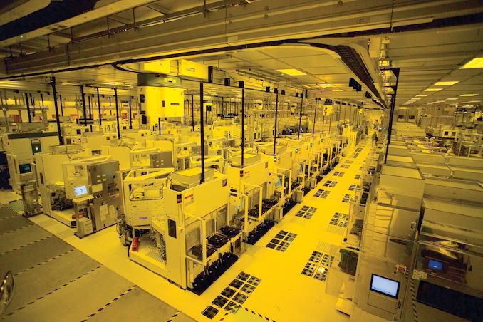

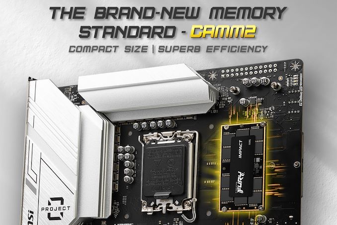
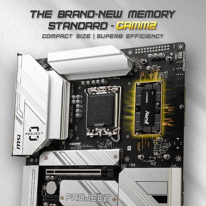

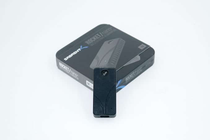



Social Plugin