
The compute market has always been hungry for memory bandwidth, particularly for high-performance applications in servers and datacenters. In recent years, the explosion in core counts per socket has further accentuated this need. Despite progress in DDR speeds, the available bandwidth per core has unfortunately not seen a corresponding scaling.

The stakeholders in the industry have been attempting to address this by building additional technology on top of existing widely-adopted memory standards. With DDR5, there are currently two technologies attempting to increase the peak bandwidth beyond the official speeds. In late 2022, SK hynix introduced MCR-DIMMs meant for operating with specific Intel server platforms. On the other hand, JEDEC - the standards-setting body - also developed specifications for MR-DIMMs with a similar approach. Both of them build upon existing DDR5 technologies by attempting to combine multiple ranks to improve peak bandwidth and latency.
The MR-DIMM standard is conceptually simple - there are multiple ranks of memory modules operating at standard DDR5 speeds with a data buffer in front. The buffer operates at 2x the speed on the host interface side, allowing for essentially double the transfer rates. The challenges obviously lie in being able to operate the logic in the host memory controller at the higher speed and keeping the power consumption / thermals in check.
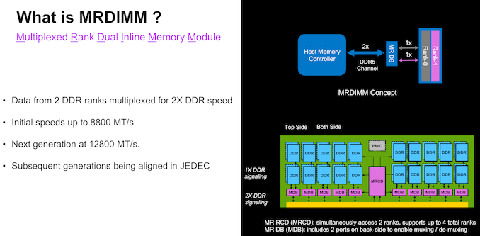
The first version of the JEDEC MR-DIMM standard specifies speeds of 8800 MT/s, with the next generation at 12800 MT/s. JEDEC also has a clear roadmap for this technology, keeping it in sync with the the improvements in the DDR5 standard.
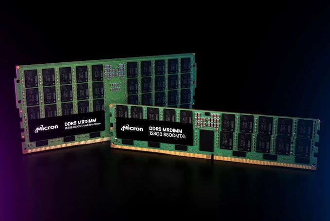
Micron and Intel have been working closely in the last few quarters to bring their former's first-generation MR-DIMM lineup to the market. Intel's Xeon 6 Family with P-Cores (Granite Rapids) is the first platform to bring MR-DIMM support at 8800 MT/s on the host side. Micron's standard-sized MR-DIMMs (suitable for 1U servers) and TFF (tall form-factor) MR-DIMMs (for 2U+ servers) have been qualified for use with the same.
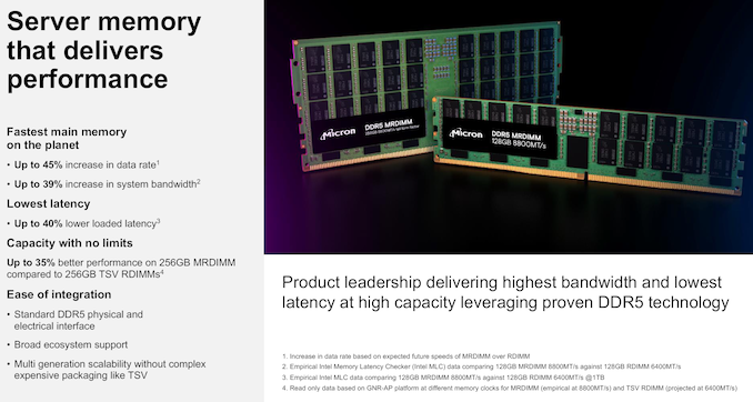
The benefits offered by MR-DIMMs are evident from the JEDEC specifications, allowing for increased data rates and system bandwidth, with improvements in latency. On the capacity side, allowing for additional ranks on the modules has enabled Micron to offer a 256 GB capacity point. It must be noted that some vendors are also using TSV (through-silicon vias) technology to to increase the per-package capacity at standard DDR5 speeds, but this adds additional cost and complexity that are largely absent in the MR-DIMM manufacturing process.
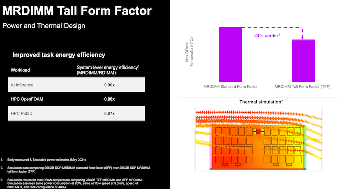
The tall form-factor (TFF) MR-DIMMs have a larger surface area compared to the standard-sized ones. For the same airflow configuration, this allows the DIMM to have a better thermal profile. This provides benefits for energy efficiency as well by reducing the possibility of thermal throttling.
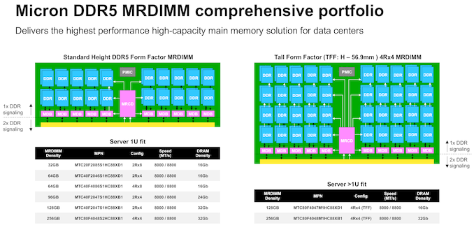
Micron is launching a comprehensive lineup of MR-DIMMs in both standard and tall form-factors today, with multiple DRAM densities and speed options as noted above.
Micron and Intel hosted a media / analyst briefing recently to demonstrate the benefits of MR-DIMMs for Xeon 6 with P-Cores (Granite Rapids). Using a 2P configuration with 96-core Xeon 6 processors, benchmarks for different ... Memory

While Realtek is best known in the enthusiast space for for its peripheral controllers such as audio codecs and network controllers, the company also has a small-but-respectable SSD controller business that tends to fly under the radar due to its focus on entry-level and mainstream drives. But Realtek's stature in the SSD space is on the rise, as the company is not only planning new PCIe Gen5 SSD controllers, but also their first high-end, DRAM-equipped SSD controller.
For this year's Computex trade show, Realtek laid out a new SSD controller roadmap that calls for the company to release a trio of new SSD controllers over the next couple of years. First up is a new four-channel entry-level PCIe 4.0 controller, the RTS5776DL, which will be joined a bit later by a PCIe 5.0 variant, the RTS5781DL. But most interesting on Realtek's new roadmap is the final chip being planned: the eight-channel, DRAM-equipped RTS5782, which would be the company's first high-end SSD controller, capable of hitting sequential read rates as high as 14GB/second.
| Realtek NVMe SSD Controller Comparison | |||||||||
| RTS5782 | RTS5781DL | RTS5776DL | RTS5772DL | RTS5766DL | |||||
| Market Segment | High-End | Mainstream | Entry-Level | ||||||
| Error Correction | 4K LDPC | 2K LDPC | |||||||
| DRAM | DDR4, LPDDR4(X) | No | No | No | No | ||||
| Host Interface | PCIe 5.0 x4 | PCIe 5.0 x4 | PCIe 4.0 x4 | PCIe 4.0 x4 | PCIe 3.0 x4 | ||||
| NVMe Version | NVMe 2.0 | NVMe 2.0 | NVMe 2.0 | NVMe 1.4 | NVMe 1.4 | ||||
| NAND Channels, Interface Speed | 8 ch, 3600 MT/s |
4 ch, 3600 MT/s |
4 ch, 3600 MT/s |
8 ch, 1600 MT/s |
4 ch, 1200 MT/s |
||||
| Sequential Read | 14 GB/s | 10 GB/s | 7.4 GB/s | 6 GB/s | 3.2 GB/s | ||||
| Sequential Write | 12 GB/s | 10 GB/s | 7.4 GB/s | 6 GB/s | 2.2 GB/s | ||||
| 4KB Random Read IOPS | 2500k | 1400k | 1200k | - | - | ||||
| 4KB Random Write IOPS | 2500k | 1400k | 1200k | - | - | ||||
Diving a bit deeper into Realtek's roadmap, the RTS5776DL is traditional DRAM-less PCIe Gen4 x4 controller with four NAND chann... SSDs

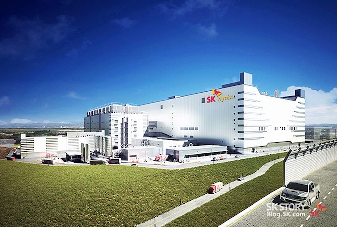
When a major industry slowdown occurs, big companies tend to slowdown their mid-term and long-term capacity related investments. This is exactly what happened to SK hynix's Yongin Semiconductor Cluster, a major project announced in April 2021 and valued at $106 billion. While development of the site has been largely completed, only 35% of the initial shell building has been constructed, according to the Korean Ministry of Trade, Industry, and Energy.
"Approximately 35% of Fab 1 has been completed so far and site renovation is in smooth progress," a statement by the Korean Ministry of Trade, Industry, and Energy reads. "By 2046, over KRW 120 trillion ($90 billion today, $106 billion in 2021) in investment will be poured to complete Fabs 1 through 4, and construction of Fab 1's production line will commence in March next year. Once completed, the infrastructure will rank as the world's largest three-story fab."
The new semiconductor fabrication cluster by SK hynix announced almost exactly three years ago is primarily meant to be used to make DRAM for PCs, mobile devices, and servers using advanced extreme ultraviolet lithography (EUV) process technologies. The cluster, located near Yongin, South Korea, is intended to consist of four large fabs situated on a 4.15 million m2 site. With a planned capacity of approximately 800,000 wafer starts per month (WSPMs), it is set to be one of the world's largest semiconductor production hubs.
With that said, SK hynix's construction progress has been slower than the company first projected. The first fab in the complex was originally meant to come online in 2025, with construction starting in the fourth quarter of 2021. However, SK hynix began to cut its capital expenditures in the second half of 2022, and the Yongin Semiconductor Cluster project fell a victim of that cut. To be sure, the site continues to be developed, just at a slower pace; which is why some 35% of the first fab shell has been built at this point.
If completed as planned in 2021, the first phase of SK hynix Yongin operations would have been a major memory production facility costing $25 billion, equipped with EUV tools, and capable of 200,000-WSPM, according to reports from 2021.
Sources: Korean Ministry of Trade, Industry, and Energy; ComputerBase
Memory
In what started last year as a handful of reports about instability with Intel's Raptor Lake desktop chips has, over the last several months, grown into a much larger saga. Facing their biggest client chip instability impediment in decades, Intel has been under increasing pressure to figure out the root cause of the issue and fix it, as claims of damaged chips have stacked up and rumors have swirled amidst the silence from Intel. But, at long last, it looks like Intel's latest saga is about to reach its end, as today the company has announced that they've found the cause of the issue, and will be rolling out a microcode fix next month to resolve it.
Officially, Intel has been working to identify the cause of desktop Raptor Lake’s instability issues since at least February of this year, if not sooner. In the interim they have discovered a couple of correlating factors – telling motherboard vendors to stop using ridiculous power settings for their out-of-the-box configurations, and finding a voltage-related bug in Enhanced Thermal Velocity Boost (eTVB) – but neither factor was the smoking gun that set all of this into motion. All of which had left Intel to continue searching for the root cause in private, and lots of awkward silence to fill the gaps in the public.
But it looks like Intel’s search has finally come to an end – even if Intel isn’t putting the smoking gun on public display quite yet. According to a fresh update posted to the company’s community website, Intel has determined the root cause at last, and has a fix in the works.
Per the company’s announcement, Intel has tracked down the cause of the instability issue to “elevated operating voltages”, that at its heart, stems from a flawed algorithm in Intel’s microcode that requested the wrong voltage. Consequently, Intel will be able to resolve the issue through a new microcode update, which pending validation, is expected to be released in the middle of August.
And while there’s nothing good for Intel about Raptor Lake’s instability issues or the need to fix them, that the problem can be ascribed to (or at least fixed by) microcode is about the best possible outcome the company could hope for. Across the full spectrum of potential causes, microcode is the easiest to fix at scale – microcode updates are already distributed through OS updates, and all chips of a given stepping (millions in all) run the same microcode. Even a motherboard BIOS-related issue would be much harder to fix given the vast number of different boards out there, never mind a true hardware flaw that would require Intel to replace even more chips than they already have.
Still, we’d also be remiss if we didn’t note that microcode is regularly used to paper over issues further down in the processor, as we’ve most famously seen with the Meltdown/Spectre fixes several years ago. So while Intel is publicly attributing the issue to microcode bugs, there are several more layers to the onion that is modern CPUs that could be playing a part. In that respect, a microcode fix grants the least amoun... CPUs

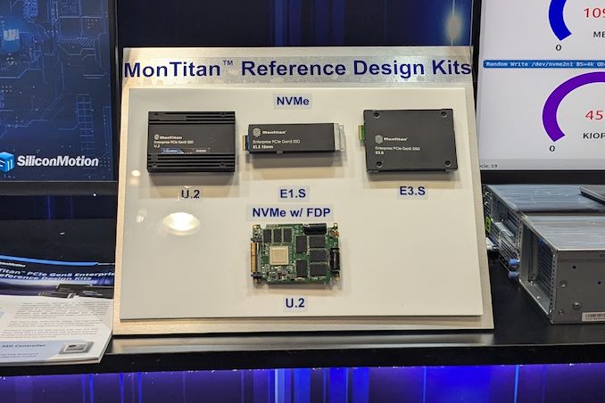
At FMS 2024, the technological requirements from the storage and memory subsystem took center stage. Both SSD and controller vendors had various demonstrations touting their suitability for different stages of the AI data pipeline - ingestion, preparation, training, checkpointing, and inference. Vendors like Solidigm have different types of SSDs optimized for different stages of the pipeline. At the same time, controller vendors have taken advantage of one of the features introduced recently in the NVM Express standard - Flexible Data Placement (FDP).
FDP involves the host providing information / hints about the areas where the controller could place the incoming write data in order to reduce the write amplification. These hints are generated based on specific block sizes advertised by the device. The feature is completely backwards-compatible, with non-FDP hosts working just as before with FDP-enabled SSDs, and vice-versa.
Silicon Motion's MonTitan Gen 5 Enterprise SSD Platform was announced back in 2022. Since then, Silicon Motion has been touting the flexibility of the platform, allowing its customers to incorporate their own features as part of the customization process. This approach is common in the enterprise space, as we have seen with Marvell's Bravera SC5 SSD controller in the DapuStor SSDs and Microchip's Flashtec controllers in the Longsys FORESEE enterprise SSDs.
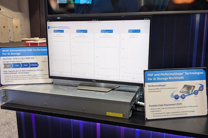
At FMS 2024, the company was demonstrating the advantages of flexible data placement by allowing a single QLC SSD based on their MonTitan platform to take part in different stages of the AI data pipeline while maintaining the required quality of service (minimum bandwidth) for each process. The company even has a trademarked name (PerformaShape) for the firmware feature in the controller that allows the isolation of different concurrent SSD accesses (from different stages in the AI data pipeline) to guarantee this QoS. Silicon Motion claims that this scheme will enable its customers to get the maximum write performance possible from QLC SSDs without negatively impacting the performance of other types of accesses.
Silicon Motion and Phison have market leadership in the client SSD controller market with similar approaches. However, their enterprise SSD controller marketing couldn't be more different. While Phison has gone in for a turnkey solution with their Gen 5 SSD platform (to the extent of not adopting the white label route for this generation, and instead opting to get the SSDs qualified with different cloud service providers themselves), Silicon Motion is opting for a different approach. The flexibility and customization possibilities can make platforms like the MonTitan appeal to flash array vendors.
Storage
While Realtek is best known in the enthusiast space for for its peripheral controllers such as audio codecs and network controllers, the company also has a small-but-respectable SSD controller business that tends to fly under the radar due to its focus on entry-level and mainstream drives. But Realtek's stature in the SSD space is on the rise, as the company is not only planning new PCIe Gen5 SSD controllers, but also their first high-end, DRAM-equipped SSD controller.
For this year's Computex trade show, Realtek laid out a new SSD controller roadmap that calls for the company to release a trio of new SSD controllers over the next couple of years. First up is a new four-channel entry-level PCIe 4.0 controller, the RTS5776DL, which will be joined a bit later by a PCIe 5.0 variant, the RTS5781DL. But most interesting on Realtek's new roadmap is the final chip being planned: the eight-channel, DRAM-equipped RTS5782, which would be the company's first high-end SSD controller, capable of hitting sequential read rates as high as 14GB/second.
| Realtek NVMe SSD Controller Comparison | |||||||||
| RTS5782 | RTS5781DL | RTS5776DL | RTS5772DL | RTS5766DL | |||||
| Market Segment | High-End | Mainstream | Entry-Level | ||||||
| Error Correction | 4K LDPC | 2K LDPC | |||||||
| DRAM | DDR4, LPDDR4(X) | No | No | No | No | ||||
| Host Interface | PCIe 5.0 x4 | PCIe 5.0 x4 | PCIe 4.0 x4 | PCIe 4.0 x4 | PCIe 3.0 x4 | ||||
| NVMe Version | NVMe 2.0 | NVMe 2.0 | NVMe 2.0 | NVMe 1.4 | NVMe 1.4 | ||||
| NAND Channels, Interface Speed | 8 ch, 3600 MT/s |
4 ch, 3600 MT/s |
4 ch, 3600 MT/s |
8 ch, 1600 MT/s |
4 ch, 1200 MT/s |
||||
| Sequential Read | 14 GB/s | 10 GB/s | 7.4 GB/s | 6 GB/s | 3.2 GB/s | ||||
| Sequential Write | 12 GB/s | 10 GB/s | 7.4 GB/s | 6 GB/s | 2.2 GB/s | ||||
| 4KB Random Read IOPS | 2500k | 1400k | 1200k | - | - | ||||
| 4KB Random Write IOPS | 2500k | 1400k | 1200k | - | - | ||||
Diving a bit deeper into Realtek's roadmap, the RTS5776DL is traditional DRAM-less PCIe Gen4 x4 controller with four NAND chann... SSDs
When a major industry slowdown occurs, big companies tend to slowdown their mid-term and long-term capacity related investments. This is exactly what happened to SK hynix's Yongin Semiconductor Cluster, a major project announced in April 2021 and valued at $106 billion. While development of the site has been largely completed, only 35% of the initial shell building has been constructed, according to the Korean Ministry of Trade, Industry, and Energy.
"Approximately 35% of Fab 1 has been completed so far and site renovation is in smooth progress," a statement by the Korean Ministry of Trade, Industry, and Energy reads. "By 2046, over KRW 120 trillion ($90 billion today, $106 billion in 2021) in investment will be poured to complete Fabs 1 through 4, and construction of Fab 1's production line will commence in March next year. Once completed, the infrastructure will rank as the world's largest three-story fab."
The new semiconductor fabrication cluster by SK hynix announced almost exactly three years ago is primarily meant to be used to make DRAM for PCs, mobile devices, and servers using advanced extreme ultraviolet lithography (EUV) process technologies. The cluster, located near Yongin, South Korea, is intended to consist of four large fabs situated on a 4.15 million m2 site. With a planned capacity of approximately 800,000 wafer starts per month (WSPMs), it is set to be one of the world's largest semiconductor production hubs.
With that said, SK hynix's construction progress has been slower than the company first projected. The first fab in the complex was originally meant to come online in 2025, with construction starting in the fourth quarter of 2021. However, SK hynix began to cut its capital expenditures in the second half of 2022, and the Yongin Semiconductor Cluster project fell a victim of that cut. To be sure, the site continues to be developed, just at a slower pace; which is why some 35% of the first fab shell has been built at this point.
If completed as planned in 2021, the first phase of SK hynix Yongin operations would have been a major memory production facility costing $25 billion, equipped with EUV tools, and capable of 200,000-WSPM, according to reports from 2021.
Sources: Korean Ministry of Trade, Industry, and Energy; ComputerBase
Memory
In what started last year as a handful of reports about instability with Intel's Raptor Lake desktop chips has, over the last several months, grown into a much larger saga. Facing their biggest client chip instability impediment in decades, Intel has been under increasing pressure to figure out the root cause of the issue and fix it, as claims of damaged chips have stacked up and rumors have swirled amidst the silence from Intel. But, at long last, it looks like Intel's latest saga is about to reach its end, as today the company has announced that they've found the cause of the issue, and will be rolling out a microcode fix next month to resolve it.
Officially, Intel has been working to identify the cause of desktop Raptor Lake’s instability issues since at least February of this year, if not sooner. In the interim they have discovered a couple of correlating factors – telling motherboard vendors to stop using ridiculous power settings for their out-of-the-box configurations, and finding a voltage-related bug in Enhanced Thermal Velocity Boost (eTVB) – but neither factor was the smoking gun that set all of this into motion. All of which had left Intel to continue searching for the root cause in private, and lots of awkward silence to fill the gaps in the public.
But it looks like Intel’s search has finally come to an end – even if Intel isn’t putting the smoking gun on public display quite yet. According to a fresh update posted to the company’s community website, Intel has determined the root cause at last, and has a fix in the works.
Per the company’s announcement, Intel has tracked down the cause of the instability issue to “elevated operating voltages”, that at its heart, stems from a flawed algorithm in Intel’s microcode that requested the wrong voltage. Consequently, Intel will be able to resolve the issue through a new microcode update, which pending validation, is expected to be released in the middle of August.
And while there’s nothing good for Intel about Raptor Lake’s instability issues or the need to fix them, that the problem can be ascribed to (or at least fixed by) microcode is about the best possible outcome the company could hope for. Across the full spectrum of potential causes, microcode is the easiest to fix at scale – microcode updates are already distributed through OS updates, and all chips of a given stepping (millions in all) run the same microcode. Even a motherboard BIOS-related issue would be much harder to fix given the vast number of different boards out there, never mind a true hardware flaw that would require Intel to replace even more chips than they already have.
Still, we’d also be remiss if we didn’t note that microcode is regularly used to paper over issues further down in the processor, as we’ve most famously seen with the Meltdown/Spectre fixes several years ago. So while Intel is publicly attributing the issue to microcode bugs, there are several more layers to the onion that is modern CPUs that could be playing a part. In that respect, a microcode fix grants the least amoun... CPUs
At FMS 2024, the technological requirements from the storage and memory subsystem took center stage. Both SSD and controller vendors had various demonstrations touting their suitability for different stages of the AI data pipeline - ingestion, preparation, training, checkpointing, and inference. Vendors like Solidigm have different types of SSDs optimized for different stages of the pipeline. At the same time, controller vendors have taken advantage of one of the features introduced recently in the NVM Express standard - Flexible Data Placement (FDP).
FDP involves the host providing information / hints about the areas where the controller could place the incoming write data in order to reduce the write amplification. These hints are generated based on specific block sizes advertised by the device. The feature is completely backwards-compatible, with non-FDP hosts working just as before with FDP-enabled SSDs, and vice-versa.
Silicon Motion's MonTitan Gen 5 Enterprise SSD Platform was announced back in 2022. Since then, Silicon Motion has been touting the flexibility of the platform, allowing its customers to incorporate their own features as part of the customization process. This approach is common in the enterprise space, as we have seen with Marvell's Bravera SC5 SSD controller in the DapuStor SSDs and Microchip's Flashtec controllers in the Longsys FORESEE enterprise SSDs.
At FMS 2024, the company was demonstrating the advantages of flexible data placement by allowing a single QLC SSD based on their MonTitan platform to take part in different stages of the AI data pipeline while maintaining the required quality of service (minimum bandwidth) for each process. The company even has a trademarked name (PerformaShape) for the firmware feature in the controller that allows the isolation of different concurrent SSD accesses (from different stages in the AI data pipeline) to guarantee this QoS. Silicon Motion claims that this scheme will enable its customers to get the maximum write performance possible from QLC SSDs without negatively impacting the performance of other types of accesses.
Silicon Motion and Phison have market leadership in the client SSD controller market with similar approaches. However, their enterprise SSD controller marketing couldn't be more different. While Phison has gone in for a turnkey solution with their Gen 5 SSD platform (to the extent of not adopting the white label route for this generation, and instead opting to get the SSDs qualified with different cloud service providers themselves), Silicon Motion is opting for a different approach. The flexibility and customization possibilities can make platforms like the MonTitan appeal to flash array vendors.
Storage

Samsung had quietly launched its BM1743 enterprise QLC SSD last month with a hefty 61.44 TB SKU. At FMS 2024, the company had the even larger 122.88 TB version of that SSD on display, alongside a few recorded benchmarking sessions. Compared to the previous generation, the BM1743 comes with a 4.1x improvement in I/O performance, improvement in data retention, and a 45% improvement in power efficiency for sequential writes.

The 128 TB-class QLC SSD boasts of sequential read speeds of 7.5 GBps and write speeds of 3 GBps. Random reads come in at 1.6 M IOPS, while 16 KB random writes clock in at 45K IOPS. Based on the quoted random write access granularity, it appears that Samsung is using a 16 KB indirection unit (IU) to optimize flash management. This is similar to the strategy adopted by Solidigm with IUs larger than 4K in their high-capacity SSDs.
A recorded benchmark session on the company's PM9D3a 8-channel Gen 5 SSD was also on display.

The SSD family is being promoted as a mainstream option for datacenters, and boasts of sequential reads up to 12 GBps and writes up to 6.8 GBps. Random reads clock in at 2 M IOPS, and random writes at 400 K IOPS.

Available in multiple form-factors up to 32 TB (M.2 tops out at 2 TB), the drive's firmware includes optional support for flexible data placement (FDP) to help address the write amplification aspect.
The PM1753 is the current enterprise SSD flagship in Samsung's lineup. With support for 16 NAND channels and capacities up to 32 TB, this U.2 / E3.S SSD has advertised sequential read and write speeds of 14.8 GBps and 11 GBps respectively. Random reads and writes for 4 KB accesses are listed at 3.4 M and 600 K IOPS.

Samsung claims a 1.7x performance improvement and a 1.7x power efficiency improvement over the previous generation (PM1743), making this TLC SSD suitable for AI servers.
The 9th Gen. V-NAND wafer was also available for viewing, though photography was prohibited. Mass production of this flash memory began in April 2024.
Storage

When Western Digital introduced its Ultrastar DC SN861 SSDs earlier this year, the company did not disclose which controller it used for these drives, which made many observers presume that WD was using an in-house controller. But a recent teardown of the drive shows that is not the case; instead, the company is using a controller from Fadu, a South Korean company founded in 2015 that specializes on enterprise-grade turnkey SSD solutions.
The Western Digital Ultrastar DC SN861 SSD is aimed at performance-hungry hyperscale datacenters and enterprise customers which are adopting PCIe Gen5 storage devices these days. And, as uncovered in photos from a recent Storage Review article, the drive is based on Fadu's FC5161 NVMe 2.0-compliant controller. The FC5161 utilizes 16 NAND channels supporting an ONFi 5.0 2400 MT/s interface, and features a combination of enterprise-grade capabilities (OCP Cloud Spec 2.0, SR-IOV, up to 512 name spaces for ZNS support, flexible data placement, NVMe-MI 1.2, advanced security, telemetry, power loss protection) not available on other off-the-shelf controllers – or on any previous Western Digital controllers.
The Ultrastar DC SN861 SSD offers sequential read speeds up to 13.7 GB/s as well as sequential write speeds up to 7.5 GB/s. As for random performance, it boasts with an up to 3.3 million random 4K read IOPS and up to 0.8 million random 4K write IOPS. The drives are available in capacities between 1.6 TB and 7.68 TB with one or three drive writes per day (DWPD) over five years rating as well as in U.2 and E1.S form-factors.
While the two form factors of the SN861 share a similar technical design, Western Digital has tailored each version for distinct workloads: the E1.S supports FDP and performance enhancements specifically for cloud environments. By contrast, the U.2 model is geared towards high-performance enterprise tasks and emerging applications like AI.
Without any doubts, Western Digital's Ultrastar DC SN861 is a feature-rich high-performance enterprise-grade SSD. It has another distinctive feature: a 5W idle power consumption, which is rather low by the standards of enterprise-grade drives (e.g., it is 1W lower compared to the SN840). While the difference with predecessors may be just 1W, hyperscalers deploy thousands of drives and for their TCO every watt counts.
Western Digital's Ultrastar DC SN861 SSDs are now available for purchase to select customers (such as Meta) and to interested parties. Prices are unknown, but they will depend on such factors as volumes.
Sources: Fadu, Storage Review
Storage
For our second keynote of the day for Computex, we have the 4th Musketeer of the great PC powers, Qualcomm. Slated to be the most PC-focused of the four keynotes, company CEO Cristiano Amon will be presenting a keynote entitled “The PC Reborn.” And while Amon is no stranger to giving keynotes, this is slated to be his most PC-centric keynote yet, giving Computex attendees a clearer idea of how focused Qualcomm will be on the PC market with their new Windows-on-Arm SoCs.
The big focus for today's keynote is expected to be the Snapdragon X Elite and X Plus SoCs, which Qualcomm announced over half a year ago, and has been touting ever since. Now, the first consumer devices based on these chips are just a couple of weeks away from shipping, so Qualcomm is in their final promotional push for their new Windows-on-Arm platform. As a result, Qualcomm should have a lot more hardware to show off, with final silicon and shipping SKUs already defined.
While Snapdragon X is not Qualcomm’s first effort to ship an Arm-based SoC for Windows devices – there are 3 generations of 8cx Gen 3 platforms that everyone is happy never to mention again – the Snapdragon X is Qualcomm’s most serious effort yet. At its core is the new, high-performance/high-efficiency Oryon CPU core, which combined with the rest of Qualcomm’s tried-and-true mobile hardware experience, the company is hoping to mold into a revolutionary Arm-based SoC for Windows laptops. The company is also counting on a decade of software development on Microsoft’s part to make the Windows-on-Arm ecosystem whole, not to mention as frictionless as possible.
Besides energy efficiency, Qualcomm’s other big push is on the burgeoning field of NPUs. The Snapdragon X NPU is rated to deliver 45 TOPS of INT8 performance, which makes it the first PC NPU to meet Microsoft’s hardware requirement for Windows 11 Copilot+ AI functionality. So Qualcomm is looking to leverage this time-limited opportunity to be the first to offer new functionality in the Windows space – a privilege normally reserved for Intel or AMD.
Come join us at 10:30pm PT / 01:30am ET / 05:30 UTC to get all the details.
Live Blog
At FMS 2024, the technological requirements from the storage and memory subsystem took center stage. Both SSD and controller vendors had various demonstrations touting their suitability for different stages of the AI data pipeline - ingestion, preparation, training, checkpointing, and inference. Vendors like Solidigm have different types of SSDs optimized for different stages of the pipeline. At the same time, controller vendors have taken advantage of one of the features introduced recently in the NVM Express standard - Flexible Data Placement (FDP).
FDP involves the host providing information / hints about the areas where the controller could place the incoming write data in order to reduce the write amplification. These hints are generated based on specific block sizes advertised by the device. The feature is completely backwards-compatible, with non-FDP hosts working just as before with FDP-enabled SSDs, and vice-versa.
Silicon Motion's MonTitan Gen 5 Enterprise SSD Platform was announced back in 2022. Since then, Silicon Motion has been touting the flexibility of the platform, allowing its customers to incorporate their own features as part of the customization process. This approach is common in the enterprise space, as we have seen with Marvell's Bravera SC5 SSD controller in the DapuStor SSDs and Microchip's Flashtec controllers in the Longsys FORESEE enterprise SSDs.
At FMS 2024, the company was demonstrating the advantages of flexible data placement by allowing a single QLC SSD based on their MonTitan platform to take part in different stages of the AI data pipeline while maintaining the required quality of service (minimum bandwidth) for each process. The company even has a trademarked name (PerformaShape) for the firmware feature in the controller that allows the isolation of different concurrent SSD accesses (from different stages in the AI data pipeline) to guarantee this QoS. Silicon Motion claims that this scheme will enable its customers to get the maximum write performance possible from QLC SSDs without negatively impacting the performance of other types of accesses.
Silicon Motion and Phison have market leadership in the client SSD controller market with similar approaches. However, their enterprise SSD controller marketing couldn't be more different. While Phison has gone in for a turnkey solution with their Gen 5 SSD platform (to the extent of not adopting the white label route for this generation, and instead opting to get the SSDs qualified with different cloud service providers themselves), Silicon Motion is opting for a different approach. The flexibility and customization possibilities can make platforms like the MonTitan appeal to flash array vendors.
Storage
Lorem Ipsum is simply dummy text of the printing and typesetting industry. Lorem Ipsum has been the industry's.
While Realtek is best known in the enthusiast space for for its peripheral controllers such as audio codecs and network controllers, the company also has a small-but-respectable SSD controller business that tends to fly under the radar due to its focus on entry-level and mainstream drives. But Realtek's stature in the SSD space is on the rise, as the company is not only planning new PCIe Gen5 SSD controllers, but also their first high-end, DRAM-equipped SSD controller.
For this year's Computex trade show, Realtek laid out a new SSD controller roadmap that calls for the company to release a trio of new SSD controllers over the next couple of years. First up is a new four-channel entry-level PCIe 4.0 controller, the RTS5776DL, which will be joined a bit later by a PCIe 5.0 variant, the RTS5781DL. But most interesting on Realtek's new roadmap is the final chip being planned: the eight-channel, DRAM-equipped RTS5782, which would be the company's first high-end SSD controller, capable of hitting sequential read rates as high as 14GB/second.
| Realtek NVMe SSD Controller Comparison | |||||||||
| RTS5782 | RTS5781DL | RTS5776DL | RTS5772DL | RTS5766DL | |||||
| Market Segment | High-End | Mainstream | Entry-Level | ||||||
| Error Correction | 4K LDPC | 2K LDPC | |||||||
| DRAM | DDR4, LPDDR4(X) | No | No | No | No | ||||
| Host Interface | PCIe 5.0 x4 | PCIe 5.0 x4 | PCIe 4.0 x4 | PCIe 4.0 x4 | PCIe 3.0 x4 | ||||
| NVMe Version | NVMe 2.0 | NVMe 2.0 | NVMe 2.0 | NVMe 1.4 | NVMe 1.4 | ||||
| NAND Channels, Interface Speed | 8 ch, 3600 MT/s |
4 ch, 3600 MT/s |
4 ch, 3600 MT/s |
8 ch, 1600 MT/s |
4 ch, 1200 MT/s |
||||
| Sequential Read | 14 GB/s | 10 GB/s | 7.4 GB/s | 6 GB/s | 3.2 GB/s | ||||
| Sequential Write | 12 GB/s | 10 GB/s | 7.4 GB/s | 6 GB/s | 2.2 GB/s | ||||
| 4KB Random Read IOPS | 2500k | 1400k | 1200k | - | - | ||||
| 4KB Random Write IOPS | 2500k | 1400k | 1200k | - | - | ||||
Diving a bit deeper into Realtek's roadmap, the RTS5776DL is traditional DRAM-less PCIe Gen4 x4 controller with four NAND chann... SSDs
When a major industry slowdown occurs, big companies tend to slowdown their mid-term and long-term capacity related investments. This is exactly what happened to SK hynix's Yongin Semiconductor Cluster, a major project announced in April 2021 and valued at $106 billion. While development of the site has been largely completed, only 35% of the initial shell building has been constructed, according to the Korean Ministry of Trade, Industry, and Energy.
"Approximately 35% of Fab 1 has been completed so far and site renovation is in smooth progress," a statement by the Korean Ministry of Trade, Industry, and Energy reads. "By 2046, over KRW 120 trillion ($90 billion today, $106 billion in 2021) in investment will be poured to complete Fabs 1 through 4, and construction of Fab 1's production line will commence in March next year. Once completed, the infrastructure will rank as the world's largest three-story fab."
The new semiconductor fabrication cluster by SK hynix announced almost exactly three years ago is primarily meant to be used to make DRAM for PCs, mobile devices, and servers using advanced extreme ultraviolet lithography (EUV) process technologies. The cluster, located near Yongin, South Korea, is intended to consist of four large fabs situated on a 4.15 million m2 site. With a planned capacity of approximately 800,000 wafer starts per month (WSPMs), it is set to be one of the world's largest semiconductor production hubs.
With that said, SK hynix's construction progress has been slower than the company first projected. The first fab in the complex was originally meant to come online in 2025, with construction starting in the fourth quarter of 2021. However, SK hynix began to cut its capital expenditures in the second half of 2022, and the Yongin Semiconductor Cluster project fell a victim of that cut. To be sure, the site continues to be developed, just at a slower pace; which is why some 35% of the first fab shell has been built at this point.
If completed as planned in 2021, the first phase of SK hynix Yongin operations would have been a major memory production facility costing $25 billion, equipped with EUV tools, and capable of 200,000-WSPM, according to reports from 2021.
Sources: Korean Ministry of Trade, Industry, and Energy; ComputerBase
Memory
In what started last year as a handful of reports about instability with Intel's Raptor Lake desktop chips has, over the last several months, grown into a much larger saga. Facing their biggest client chip instability impediment in decades, Intel has been under increasing pressure to figure out the root cause of the issue and fix it, as claims of damaged chips have stacked up and rumors have swirled amidst the silence from Intel. But, at long last, it looks like Intel's latest saga is about to reach its end, as today the company has announced that they've found the cause of the issue, and will be rolling out a microcode fix next month to resolve it.
Officially, Intel has been working to identify the cause of desktop Raptor Lake’s instability issues since at least February of this year, if not sooner. In the interim they have discovered a couple of correlating factors – telling motherboard vendors to stop using ridiculous power settings for their out-of-the-box configurations, and finding a voltage-related bug in Enhanced Thermal Velocity Boost (eTVB) – but neither factor was the smoking gun that set all of this into motion. All of which had left Intel to continue searching for the root cause in private, and lots of awkward silence to fill the gaps in the public.
But it looks like Intel’s search has finally come to an end – even if Intel isn’t putting the smoking gun on public display quite yet. According to a fresh update posted to the company’s community website, Intel has determined the root cause at last, and has a fix in the works.
Per the company’s announcement, Intel has tracked down the cause of the instability issue to “elevated operating voltages”, that at its heart, stems from a flawed algorithm in Intel’s microcode that requested the wrong voltage. Consequently, Intel will be able to resolve the issue through a new microcode update, which pending validation, is expected to be released in the middle of August.
And while there’s nothing good for Intel about Raptor Lake’s instability issues or the need to fix them, that the problem can be ascribed to (or at least fixed by) microcode is about the best possible outcome the company could hope for. Across the full spectrum of potential causes, microcode is the easiest to fix at scale – microcode updates are already distributed through OS updates, and all chips of a given stepping (millions in all) run the same microcode. Even a motherboard BIOS-related issue would be much harder to fix given the vast number of different boards out there, never mind a true hardware flaw that would require Intel to replace even more chips than they already have.
Still, we’d also be remiss if we didn’t note that microcode is regularly used to paper over issues further down in the processor, as we’ve most famously seen with the Meltdown/Spectre fixes several years ago. So while Intel is publicly attributing the issue to microcode bugs, there are several more layers to the onion that is modern CPUs that could be playing a part. In that respect, a microcode fix grants the least amoun... CPUs
 is the first platform to bring MR-DIMM support at 8800 MT/s on the host side. Micron's standard-sized MR-DIMMs (suitable for 1U servers) and TFF (tall form-factor) MR-DIMMs (for 2U+ servers) have been qualified for use with the same.</p>
<p align="center"><a href="https://www.anandtech.com/show/21470/micron-mrdimm-lineup-expands-datacenter-dram-portfolio"><img alt="" src="https://images.anandtech.com/doci/21470/micron-mrdimm-lineup-intro_575px.png" /></a></p>
<p>The benefits offered by MR-DIMMs are evident from the JEDEC specifications, allowing for increased data rates and system bandwidth, with improvements in latency. On the capacity side, allowing for additional ranks on the modules has enabled Micron to offer a 256 GB capacity point. It must be noted that some vendors are also using TSV (through-silicon vias) technology to to increase the per-package capacity at standard DDR5 speeds, but this adds additional cost and complexity that are largely absent in the MR-DIMM manufacturing process.</p>
<p align="center"><a href="https://www.anandtech.com/show/21470/micron-mrdimm-lineup-expands-datacenter-dram-portfolio"><img alt="" src="https://images.anandtech.com/doci/21470/micron-mrdimm-tff-benefits_575px.png" /></a></p>
<p>The tall form-factor (TFF) MR-DIMMs have a larger surface area compared to the standard-sized ones. For the same airflow configuration, this allows the DIMM to have a better thermal profile. This provides benefits for energy efficiency as well by reducing the possibility of thermal throttling.</p>
<p align="center"><a href="https://www.anandtech.com/show/21470/micron-mrdimm-lineup-expands-datacenter-dram-portfolio"><img alt="" src="https://images.anandtech.com/doci/21470/micron-mrdimm-lineup-skus_575px.png" /></a></p>
<p>Micron is launching a comprehensive lineup of MR-DIMMs in both standard and tall form-factors today, with multiple DRAM densities and speed options as noted above.</p>
<h3>MRDIMM Benefits - Intel Granite Rapids Gets a Performance Boost</h3>
<p>Micron and Intel hosted a media / analyst briefing recently to demonstrate the benefits of MR-DIMMs for Xeon 6 with P-Cores (Granite Rapids). Using a 2P configuration with 96-core Xeon 6 processors, benchmarks for different ... Memory)
 is the first platform to bring MR-DIMM support at 8800 MT/s on the host side. Micron's standard-sized MR-DIMMs (suitable for 1U servers) and TFF (tall form-factor) MR-DIMMs (for 2U+ servers) have been qualified for use with the same.</p>
<p align="center"><a href="https://www.anandtech.com/show/21470/micron-mrdimm-lineup-expands-datacenter-dram-portfolio"><img alt="" src="https://images.anandtech.com/doci/21470/micron-mrdimm-lineup-intro_575px.png" /></a></p>
<p>The benefits offered by MR-DIMMs are evident from the JEDEC specifications, allowing for increased data rates and system bandwidth, with improvements in latency. On the capacity side, allowing for additional ranks on the modules has enabled Micron to offer a 256 GB capacity point. It must be noted that some vendors are also using TSV (through-silicon vias) technology to to increase the per-package capacity at standard DDR5 speeds, but this adds additional cost and complexity that are largely absent in the MR-DIMM manufacturing process.</p>
<p align="center"><a href="https://www.anandtech.com/show/21470/micron-mrdimm-lineup-expands-datacenter-dram-portfolio"><img alt="" src="https://images.anandtech.com/doci/21470/micron-mrdimm-tff-benefits_575px.png" /></a></p>
<p>The tall form-factor (TFF) MR-DIMMs have a larger surface area compared to the standard-sized ones. For the same airflow configuration, this allows the DIMM to have a better thermal profile. This provides benefits for energy efficiency as well by reducing the possibility of thermal throttling.</p>
<p align="center"><a href="https://www.anandtech.com/show/21470/micron-mrdimm-lineup-expands-datacenter-dram-portfolio"><img alt="" src="https://images.anandtech.com/doci/21470/micron-mrdimm-lineup-skus_575px.png" /></a></p>
<p>Micron is launching a comprehensive lineup of MR-DIMMs in both standard and tall form-factors today, with multiple DRAM densities and speed options as noted above.</p>
<h3>MRDIMM Benefits - Intel Granite Rapids Gets a Performance Boost</h3>
<p>Micron and Intel hosted a media / analyst briefing recently to demonstrate the benefits of MR-DIMMs for Xeon 6 with P-Cores (Granite Rapids). Using a 2P configuration with 96-core Xeon 6 processors, benchmarks for different ... Memory | https://compbuddey.blogspot.com/2024/08/micron-expands-datacenter-dram_4.html)
 is the first platform to bring MR-DIMM support at 8800 MT/s on the host side. Micron's standard-sized MR-DIMMs (suitable for 1U servers) and TFF (tall form-factor) MR-DIMMs (for 2U+ servers) have been qualified for use with the same.</p>
<p align="center"><a href="https://www.anandtech.com/show/21470/micron-mrdimm-lineup-expands-datacenter-dram-portfolio"><img alt="" src="https://images.anandtech.com/doci/21470/micron-mrdimm-lineup-intro_575px.png" /></a></p>
<p>The benefits offered by MR-DIMMs are evident from the JEDEC specifications, allowing for increased data rates and system bandwidth, with improvements in latency. On the capacity side, allowing for additional ranks on the modules has enabled Micron to offer a 256 GB capacity point. It must be noted that some vendors are also using TSV (through-silicon vias) technology to to increase the per-package capacity at standard DDR5 speeds, but this adds additional cost and complexity that are largely absent in the MR-DIMM manufacturing process.</p>
<p align="center"><a href="https://www.anandtech.com/show/21470/micron-mrdimm-lineup-expands-datacenter-dram-portfolio"><img alt="" src="https://images.anandtech.com/doci/21470/micron-mrdimm-tff-benefits_575px.png" /></a></p>
<p>The tall form-factor (TFF) MR-DIMMs have a larger surface area compared to the standard-sized ones. For the same airflow configuration, this allows the DIMM to have a better thermal profile. This provides benefits for energy efficiency as well by reducing the possibility of thermal throttling.</p>
<p align="center"><a href="https://www.anandtech.com/show/21470/micron-mrdimm-lineup-expands-datacenter-dram-portfolio"><img alt="" src="https://images.anandtech.com/doci/21470/micron-mrdimm-lineup-skus_575px.png" /></a></p>
<p>Micron is launching a comprehensive lineup of MR-DIMMs in both standard and tall form-factors today, with multiple DRAM densities and speed options as noted above.</p>
<h3>MRDIMM Benefits - Intel Granite Rapids Gets a Performance Boost</h3>
<p>Micron and Intel hosted a media / analyst briefing recently to demonstrate the benefits of MR-DIMMs for Xeon 6 with P-Cores (Granite Rapids). Using a 2P configuration with 96-core Xeon 6 processors, benchmarks for different ... Memory&body=https://compbuddey.blogspot.com/2024/08/micron-expands-datacenter-dram_4.html)
0 Comments