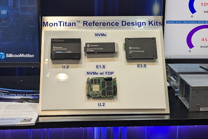

At FMS 2024, the technological requirements from the storage and memory subsystem took center stage. Both SSD and controller vendors had various demonstrations touting their suitability for different stages of the AI data pipeline - ingestion, preparation, training, checkpointing, and inference. Vendors like Solidigm have different types of SSDs optimized for different stages of the pipeline. At the same time, controller vendors have taken advantage of one of the features introduced recently in the NVM Express standard - Flexible Data Placement (FDP).
FDP involves the host providing information / hints about the areas where the controller could place the incoming write data in order to reduce the write amplification. These hints are generated based on specific block sizes advertised by the device. The feature is completely backwards-compatible, with non-FDP hosts working just as before with FDP-enabled SSDs, and vice-versa.
Silicon Motion's MonTitan Gen 5 Enterprise SSD Platform was announced back in 2022. Since then, Silicon Motion has been touting the flexibility of the platform, allowing its customers to incorporate their own features as part of the customization process. This approach is common in the enterprise space, as we have seen with Marvell's Bravera SC5 SSD controller in the DapuStor SSDs and Microchip's Flashtec controllers in the Longsys FORESEE enterprise SSDs.
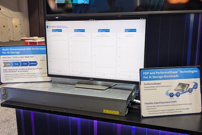
At FMS 2024, the company was demonstrating the advantages of flexible data placement by allowing a single QLC SSD based on their MonTitan platform to take part in different stages of the AI data pipeline while maintaining the required quality of service (minimum bandwidth) for each process. The company even has a trademarked name (PerformaShape) for the firmware feature in the controller that allows the isolation of different concurrent SSD accesses (from different stages in the AI data pipeline) to guarantee this QoS. Silicon Motion claims that this scheme will enable its customers to get the maximum write performance possible from QLC SSDs without negatively impacting the performance of other types of accesses.
Silicon Motion and Phison have market leadership in the client SSD controller market with similar approaches. However, their enterprise SSD controller marketing couldn't be more different. While Phison has gone in for a turnkey solution with their Gen 5 SSD platform (to the extent of not adopting the white label route for this generation, and instead opting to get the SSDs qualified with different cloud service providers themselves), Silicon Motion is opting for a different approach. The flexibility and customization possibilities can make platforms like the MonTitan appeal to flash array vendors.
Storage

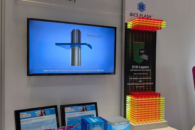
Kioxia's booth at FMS 2024 was a busy one with multiple technology demonstrations keeping visitors occupied. A walk-through of the BiCS 8 manufacturing process was the first to grab my attention. Kioxia and Western Digital announced the sampling of BiCS 8 in March 2023. We had touched briefly upon its CMOS Bonded Array (CBA) scheme in our coverage of Kioxial's 2Tb QLC NAND device and coverage of Western Digital's 128 TB QLC enterprise SSD proof-of-concept demonstration. At Kioxia's booth, we got more insights.
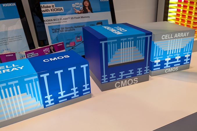
Traditionally, fabrication of flash chips involved placement of the associate logic circuitry (CMOS process) around the periphery of the flash array. The process then moved on to putting the CMOS under the cell array, but the wafer development process was serialized with the CMOS logic getting fabricated first followed by the cell array on top. However, this has some challenges because the cell array requires a high-temperature processing step to ensure higher reliability that can be detrimental to the health of the CMOS logic. Thanks to recent advancements in wafer bonding techniques, the new CBA process allows the CMOS wafer and cell array wafer to be processed independently in parallel and then pieced together, as shown in the models above.
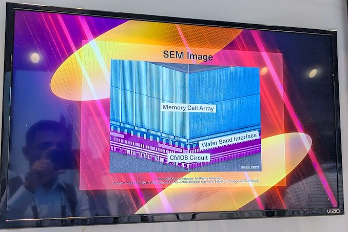
The BiCS 8 3D NAND incorporates 218 layers, compared to 112 layers in BiCS 5 and 162 layers in BiCS 6. The company decided to skip over BiCS 7 (or, rather, it was probably a short-lived generation meant as an internal test vehicle). The generation retains the four-plane charge trap structure of BiCS 6. In its TLC avatar, it is available as a 1 Tbit device. The QLC version is available in two capacities - 1 Tbit and 2 Tbit.
Kioxia also noted that while the number of layers (218) doesn't compare favorably with the latest layer counts from the competition, its lateral scaling / cell shrinkage has enabled it to be competitive in terms of bit density as well as operating speeds (3200 MT/s). For reference, the latest shipping NAND from Micron - the G9 - has 276 layers with a bit density in TLC mode of 21 Gbit/mm2, and operates at up to 3600 MT/s. However, its 232L NAND operates only up to 2400 MT/s and has a bit density of 14.6 Gbit/mm2.
It must be noted that the CBA hybrid bonding process has advantages over the current processes used by other vendors - including Micron's CMOS under array (CuA) and SK hynix's 4D PUC (periphery-under-chip) developed in the late 2010s. It is expected that other NAND vendors will also move eventually to some variant of the hybrid bonding scheme used by Kioxia.
Storage
Under the CHIPS & Science Act, the U.S. government provided tens of billions of dollars in grants and loans to the world's leading maker of chips, such as Intel, Samsung, and TSMC, which will significantly expand the country's semiconductor production industry in the coming years. However, most chips are typically tested, assembled, and packaged in Asia, which has left the American supply chain incomplete. Addressing this last gap in the government's domestic chip production plans, these past couple of weeks the U.S. government signed memorandums of understanding worth about $1.5 billion with Amkor and SK hynix to support their efforts to build chip packaging facilities in the U.S.
Amkor plans to build a $2 billion advanced packaging facility near Peoria, Arizona, to test and assemble chips produced by TSMC at its Fab 21 near Phoenix, Arizona. The company signed a MOU that offers $400 million in direct funding and access to $200 million in loans under the CHIPS & Science Act. In addition, the company plans to take advantage of a 25% investment tax credit on eligible capital expenditures.
Set to be strategically positioned near TSMC's upcoming Fab 21 complex in Arizona, Amkor's Peoria facility will occupy 55 acres and, when fully completed, will feature over 500,000 square feet (46,451 square meters) of cleanroom space, more than twice the size of Amkor's advanced packaging site in Vietnam. Although the company has not disclosed the exact capacity or the specific technologies the facility will support, it is expected to cater to a wide range of industries, including automotive, high-performance computing, and mobile technologies. This suggests the new plant will offer diverse packaging solutions, including traditional, 2.5D, and 3D technologies.
Amkor has collaborated extensively with Apple on the vision and initial setup of the Peoria facility, as Apple is slated to be the facility's first and largest customer, marking a significant commitment from the tech giant. This partnership highlights the importance of the new facility in reinforcing the U.S. semiconductor supply chain and positioning Amkor as a key partner for companies relying on TSMC's manufacturing capabilities. The project is expected to generate around 2,000 jobs and is scheduled to begin operations in 2027.
This week SK hynix also signed a preliminary agreement with the U.S. government to receive up to $450 million in direct funding and $500 million in loans to build an advanced memory packaging facility in West Lafayette, Indiana.
The proposed facility is scheduled to begin operations in 2028, which means that it will assemble HBM4 or HBM4E memory. Meanwhile, DRAM devices for high bandwidth memory (HBM) stacks will still be produced in South Korea. Nonetheless, packing finished HBM4/HBM4E in the U.S. and possibly integrating these memory modules with high-end processors is a big deal.
In addition to building its packaging plant, SK hynix plans to collaborate with Purdue University and other local research institutions to advance semiconductor technology and packaging innovations. This partnership is intended to bolster research and development in the region, positioning the facility as a hub for AI technology and skilled employment.
Semiconductors
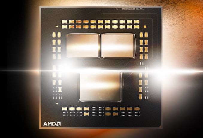
During their opening keynote at Computex 2024, AMD announced their intention to launch a pair of new Ryzen 5000 processors for their legacy AM4 platform. The new chips, both getting the XT suffix, will be the Ryzen 9 5900XT, a 16 core Zen 3 part, while the Ryzen 7 5800XT will be an 8 core Zen 3.
The new chips are intended to underscore AMD's ongoing commitment to supporting their consumer platforms over several years. And while the specification changes are rather minor overall – the Zen 3 CPU architecture has long since been taken as far as it can reasonable go – it does give AMD a chance to refresh the platform by slinging hardware at new price points. AMD did something very similar for the Ryzen 3000 generation with the late-model Ryzen 3000 XT chips.
| AMD Ryzen 5000XT Series Processors (Zen 3) |
||||||
| AnandTech | Cores / Threads |
Base Freq |
Turbo Freq |
L2 Cache |
L3 Cache |
TDP |
| Ryzen 9 5950X | 16C / 32T | 3.4 GHz | 4.9 GHz | 8 MB | 64 MB | 105 W |
| Ryzen 9 5900XT | 16C / 32T | 3.3 GHz | 4.8 GHz | 8 MB | 64 MB | 105 W |
| Ryzen 9 5900X | 12C / 24T | 3.7 GHz | 4.8 GHz | 6 MB | 64 MB | 105 W |
| Ryzen 7 5800XT | 8C / 16T | 3.8 GHz | 4.8 GHz | 4 MB | 32 MB | 105 W |
| Ryzen 7 5800X | 8C / 16T | 3.8 GHz | 4.7 GHz | 4 MB | 32 MB | 105 W |
We've dedicated many column inches covering Zen 3 and the Ryzen 5000 series since they launched in late 2020, so there isn't anything new to add here. Zen 3 is no longer AMD's latest and greatest, but the platform as a whole is quite cheap to produce, making it a viable budget offering for new builds, or offering one last upgrade for old builds.
The Ryzen 9 5900XT is a 16 core part, and isn't to be confused with the Ryzen 9 5900X, which is a 12 core part. It ships with a peak turbo clockspeed of 4.8GHz, 100 MHz lower than the top-tier Ryzen 9 5950X. This makes it's XT designation somewhat of a misnomer compared to previous generations of XT chips, although it's clear that AMD has boxed themselves into a corner with their naming scheme, as they both need a way to designate that this is a new chip, and yet still place it below the 5950X.
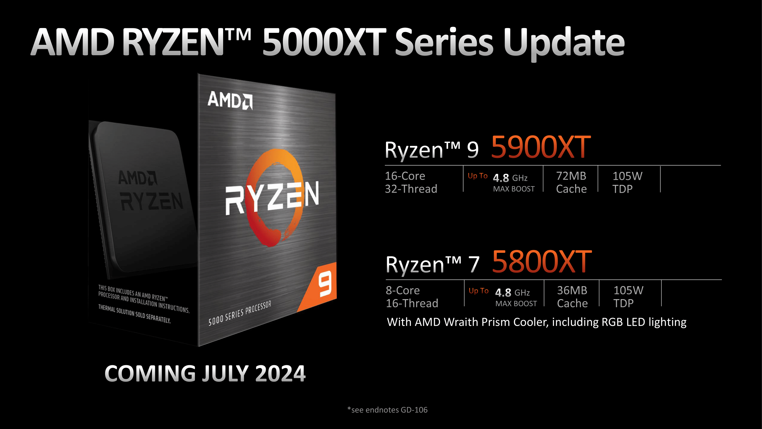
Looking at the second chip, we have the Ryzen 7 5800XT. This is an 8 core part that does improve on its predecessor, offering a 4.8GHz max turbo clock that is 100MHz higher than the Ryzen 7 5800X's. Both chips otherwise share the same characteristics, including 6 MB of L2 cache and 32 MB of L3 cache, and all four of the chips – including the two new XT series and the corresponding X series chips – all come with a 105 Watt TDP.
In terms of motherboard compatibility, all of the AM4 motherboards that currently support the Ryzen 5000 series are also compatible with the Ryzen 5000XT series, although users are likely to need to perform a firmware update to ensure maximum compatibility; they are the same chips, but the microcodes are likely different.
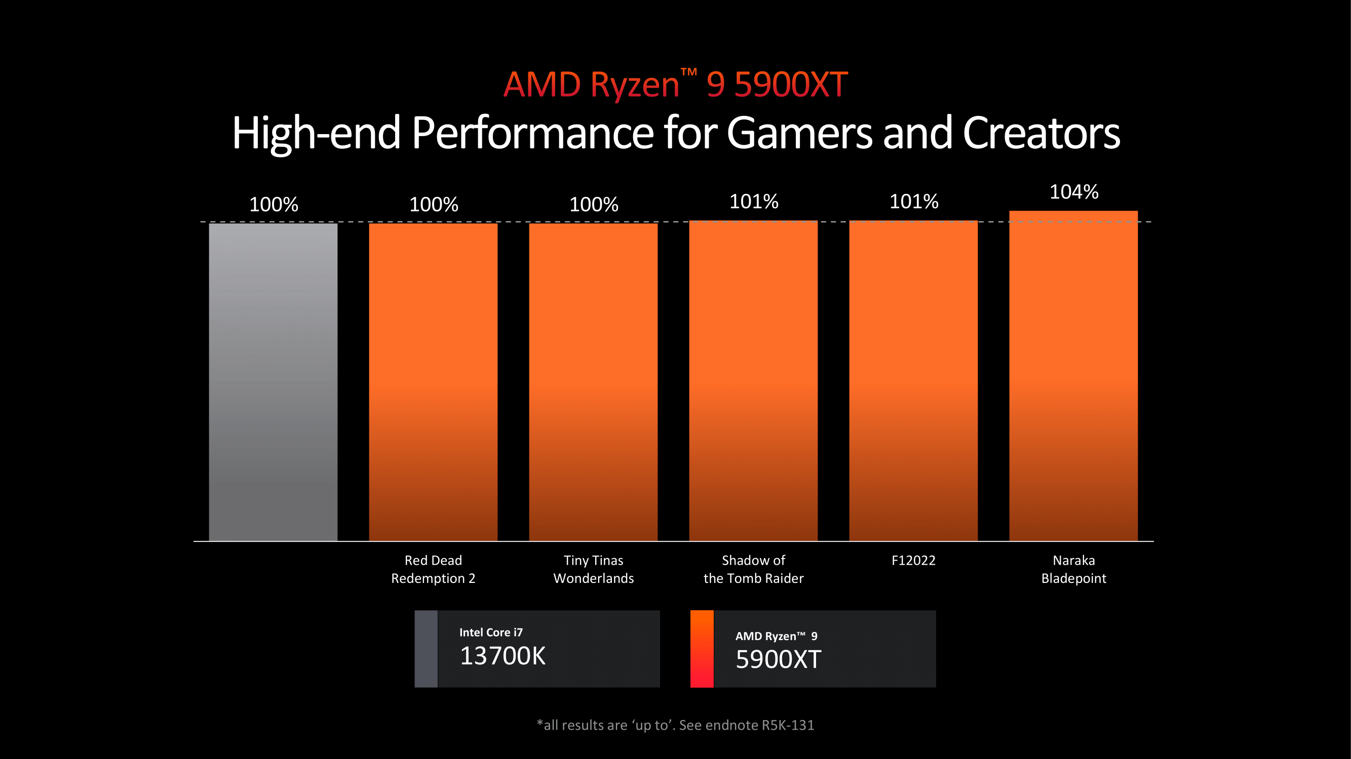
AMD has provided some gaming performance figures comparing the Ryzen 9 5900XT to Intel's 13th Gen Core i7-13700K. It does offer very modest yet marginal gains in games by up to 4%; it's not mind-blowing, but the... CPUs

Lorem Ipsum is simply dummy text of the printing and typesetting industry. Lorem Ipsum has been the industry's.



.</p>
<p>FDP involves the host providing information / hints about the areas where the controller could place the incoming write data in order to reduce the write amplification. These hints are generated based on specific block sizes advertised by the device. The feature is completely backwards-compatible, with non-FDP hosts working just as before with FDP-enabled SSDs, and vice-versa.</p>
<p>Silicon Motion's <a href="https://www.anandtech.com/show/17512/silicon-motion-sm8366-montitan-ssd-platform">MonTitan Gen 5 Enterprise SSD Platform</a> was announced back in 2022. Since then, Silicon Motion has been touting the flexibility of the platform, allowing its customers to incorporate their own features as part of the customization process. This approach is common in the enterprise space, as we have seen with Marvell's Bravera SC5 SSD controller in the DapuStor SSDs and Microchip's Flashtec controllers in the Longsys FORESEE enterprise SSDs.</p>
<p align="center"><a href="https://www.anandtech.com/show/21522/silicon-motion-demonstrates-flexible-data-placement-on-montitan-gen-5-enterprise-ssd-platform"><img alt="" src="https://images.anandtech.com/doci/21522/mid-page_575px.jpg" /></a></p>
<p>At FMS 2024, the company was demonstrating the advantages of flexible data placement by allowing a single QLC SSD based on their MonTitan platform to take part in different stages of the AI data pipeline while maintaining the required quality of service (minimum bandwidth) for each process. The company even has a trademarked name (PerformaShape) for the firmware feature in the controller that allows the isolation of different concurrent SSD accesses (from different stages in the AI data pipeline) to guarantee this QoS. Silicon Motion claims that this scheme will enable its customers to get the maximum write performance possible from QLC SSDs without negatively impacting the performance of other types of accesses.</p>
<p>Silicon Motion and Phison have market leadership in the client SSD controller market with similar approaches. However, their enterprise SSD controller marketing couldn't be more different. While Phison has gone in for a turnkey solution with their Gen 5 SSD platform (to the extent of not adopting the white label route for this generation, and instead opting to get the SSDs qualified with different cloud service providers themselves), Silicon Motion is opting for a different approach. The flexibility and customization possibilities can make platforms like the MonTitan appeal to flash array vendors.</p>
</p> Storage)
.</p>
<p>FDP involves the host providing information / hints about the areas where the controller could place the incoming write data in order to reduce the write amplification. These hints are generated based on specific block sizes advertised by the device. The feature is completely backwards-compatible, with non-FDP hosts working just as before with FDP-enabled SSDs, and vice-versa.</p>
<p>Silicon Motion's <a href="https://www.anandtech.com/show/17512/silicon-motion-sm8366-montitan-ssd-platform">MonTitan Gen 5 Enterprise SSD Platform</a> was announced back in 2022. Since then, Silicon Motion has been touting the flexibility of the platform, allowing its customers to incorporate their own features as part of the customization process. This approach is common in the enterprise space, as we have seen with Marvell's Bravera SC5 SSD controller in the DapuStor SSDs and Microchip's Flashtec controllers in the Longsys FORESEE enterprise SSDs.</p>
<p align="center"><a href="https://www.anandtech.com/show/21522/silicon-motion-demonstrates-flexible-data-placement-on-montitan-gen-5-enterprise-ssd-platform"><img alt="" src="https://images.anandtech.com/doci/21522/mid-page_575px.jpg" /></a></p>
<p>At FMS 2024, the company was demonstrating the advantages of flexible data placement by allowing a single QLC SSD based on their MonTitan platform to take part in different stages of the AI data pipeline while maintaining the required quality of service (minimum bandwidth) for each process. The company even has a trademarked name (PerformaShape) for the firmware feature in the controller that allows the isolation of different concurrent SSD accesses (from different stages in the AI data pipeline) to guarantee this QoS. Silicon Motion claims that this scheme will enable its customers to get the maximum write performance possible from QLC SSDs without negatively impacting the performance of other types of accesses.</p>
<p>Silicon Motion and Phison have market leadership in the client SSD controller market with similar approaches. However, their enterprise SSD controller marketing couldn't be more different. While Phison has gone in for a turnkey solution with their Gen 5 SSD platform (to the extent of not adopting the white label route for this generation, and instead opting to get the SSDs qualified with different cloud service providers themselves), Silicon Motion is opting for a different approach. The flexibility and customization possibilities can make platforms like the MonTitan appeal to flash array vendors.</p>
</p> Storage)
.</p>
<p>FDP involves the host providing information / hints about the areas where the controller could place the incoming write data in order to reduce the write amplification. These hints are generated based on specific block sizes advertised by the device. The feature is completely backwards-compatible, with non-FDP hosts working just as before with FDP-enabled SSDs, and vice-versa.</p>
<p>Silicon Motion's <a href="https://www.anandtech.com/show/17512/silicon-motion-sm8366-montitan-ssd-platform">MonTitan Gen 5 Enterprise SSD Platform</a> was announced back in 2022. Since then, Silicon Motion has been touting the flexibility of the platform, allowing its customers to incorporate their own features as part of the customization process. This approach is common in the enterprise space, as we have seen with Marvell's Bravera SC5 SSD controller in the DapuStor SSDs and Microchip's Flashtec controllers in the Longsys FORESEE enterprise SSDs.</p>
<p align="center"><a href="https://www.anandtech.com/show/21522/silicon-motion-demonstrates-flexible-data-placement-on-montitan-gen-5-enterprise-ssd-platform"><img alt="" src="https://images.anandtech.com/doci/21522/mid-page_575px.jpg" /></a></p>
<p>At FMS 2024, the company was demonstrating the advantages of flexible data placement by allowing a single QLC SSD based on their MonTitan platform to take part in different stages of the AI data pipeline while maintaining the required quality of service (minimum bandwidth) for each process. The company even has a trademarked name (PerformaShape) for the firmware feature in the controller that allows the isolation of different concurrent SSD accesses (from different stages in the AI data pipeline) to guarantee this QoS. Silicon Motion claims that this scheme will enable its customers to get the maximum write performance possible from QLC SSDs without negatively impacting the performance of other types of accesses.</p>
<p>Silicon Motion and Phison have market leadership in the client SSD controller market with similar approaches. However, their enterprise SSD controller marketing couldn't be more different. While Phison has gone in for a turnkey solution with their Gen 5 SSD platform (to the extent of not adopting the white label route for this generation, and instead opting to get the SSDs qualified with different cloud service providers themselves), Silicon Motion is opting for a different approach. The flexibility and customization possibilities can make platforms like the MonTitan appeal to flash array vendors.</p>
</p> Storage | https://compbuddey.blogspot.com/2025/07/silicon-motion-demonstrates-flexible_29.html)
.</p>
<p>FDP involves the host providing information / hints about the areas where the controller could place the incoming write data in order to reduce the write amplification. These hints are generated based on specific block sizes advertised by the device. The feature is completely backwards-compatible, with non-FDP hosts working just as before with FDP-enabled SSDs, and vice-versa.</p>
<p>Silicon Motion's <a href="https://www.anandtech.com/show/17512/silicon-motion-sm8366-montitan-ssd-platform">MonTitan Gen 5 Enterprise SSD Platform</a> was announced back in 2022. Since then, Silicon Motion has been touting the flexibility of the platform, allowing its customers to incorporate their own features as part of the customization process. This approach is common in the enterprise space, as we have seen with Marvell's Bravera SC5 SSD controller in the DapuStor SSDs and Microchip's Flashtec controllers in the Longsys FORESEE enterprise SSDs.</p>
<p align="center"><a href="https://www.anandtech.com/show/21522/silicon-motion-demonstrates-flexible-data-placement-on-montitan-gen-5-enterprise-ssd-platform"><img alt="" src="https://images.anandtech.com/doci/21522/mid-page_575px.jpg" /></a></p>
<p>At FMS 2024, the company was demonstrating the advantages of flexible data placement by allowing a single QLC SSD based on their MonTitan platform to take part in different stages of the AI data pipeline while maintaining the required quality of service (minimum bandwidth) for each process. The company even has a trademarked name (PerformaShape) for the firmware feature in the controller that allows the isolation of different concurrent SSD accesses (from different stages in the AI data pipeline) to guarantee this QoS. Silicon Motion claims that this scheme will enable its customers to get the maximum write performance possible from QLC SSDs without negatively impacting the performance of other types of accesses.</p>
<p>Silicon Motion and Phison have market leadership in the client SSD controller market with similar approaches. However, their enterprise SSD controller marketing couldn't be more different. While Phison has gone in for a turnkey solution with their Gen 5 SSD platform (to the extent of not adopting the white label route for this generation, and instead opting to get the SSDs qualified with different cloud service providers themselves), Silicon Motion is opting for a different approach. The flexibility and customization possibilities can make platforms like the MonTitan appeal to flash array vendors.</p>
</p> Storage&body=https://compbuddey.blogspot.com/2025/07/silicon-motion-demonstrates-flexible_29.html)


0 Comments