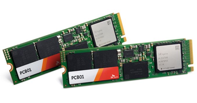

SK hynix early in Friday announced that the company has finished the development of it's PCB01 PCIe Gen5 SSD, the company's forthcoming high-end SSD for OEMs. Based on the company's new Alistar platform, the PCB01 is designed to deliver chart-topping performance for client machines. And, as a sign of the times, SK hynix is positioning the PCB01 for AI PCs, looking to synergize with the overall industry interest in anything and everything AI.
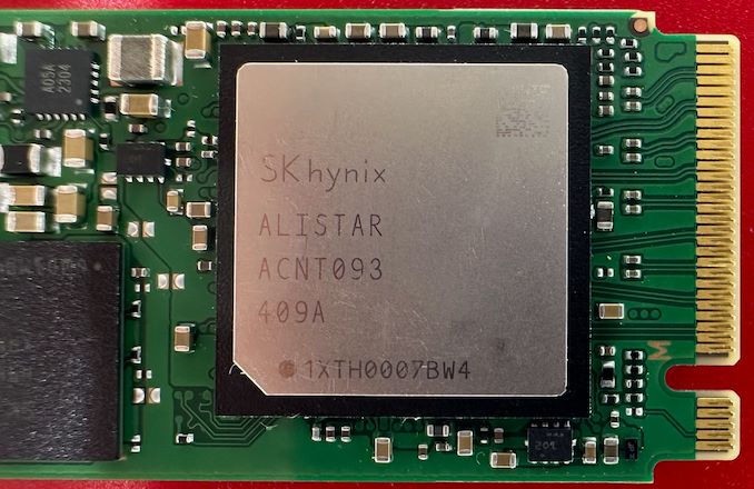
The bare, OEM-focused drives have previously been shown off by SK hynix, and make no attempt to hide what's under the hood. The PCB01 relies on SK hynix's Alistar controller, which features a PCIe Gen5 x4 host interface on the front end and eight NAND channels on the back end, placing it solidly in the realm of high-end SSDs. Paired with the Alistar controller is the company's latest 238-layer TLC NAND (H25T1TD48C & H25T2TD88C), which offers a maximum transfer speed of 2400 MT/second. Being that this is a high-end client SSD, there's also a DRAM chip on board, though the company isn't disclosing its capacity.
As with other high-end PCIe 5.0 client SSDs, SK hynix is planning on hitting peak read speeds of up to 14GB/second on the drive, while peak sequential write speeds should top 12GB/second (with pSLC caching, of course) – performance figures well within the realm of possibility for an 8 channel drive. As for random performance, at Computex the company was telling attendees that the drives should be able to sustain 4K random read and write rates of 2 million IOPS, which is very high as well. The SSDs are also said to consume up to 30% less power than 'predecessors,' according to SK hynix, though the company didn't elaborate on that figure. Typically in the storage industry, energy figures are based on iso-performance (rather than peak performance) – essentially measuring energy efficiency per bit rather than toal power consumption – and that is likely the case here as well.
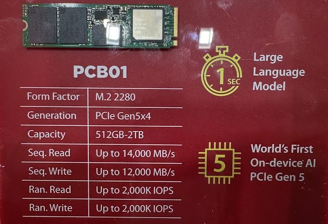
At least initially, SK Hynix plans to release its PCB01 in three capacities – 512 GB, 1 TB, and 2 TB. The company has previously disclosed that their 238L TLC NAND has a capacity of 512Gbit, so these are typical capacity figures for single-sided drives. And while the focus of the company's press release this week was on OEM drives, this is the same controller and NAND that is also going into the company's previously-teased retail Platinum P51 SSD, so this week's reveal offers a bit more detail into what to expect from that drive family as well.
Specs aside, Ahn Hyun, the Head of the N-S Committee at SK hynix, said that multiple global CPU providers for on-device AI PCs are seeking collaboration for the compatibility validation process, which is underway, so expect PCB01 drives inside PCs in this back-to-school and holiday seasons.
"We will work towards enhancing our leadership as the global top AI memory provider also in the NAND solution space by successfully completing the customer validation and mass production of PCB01, which will be in the limelight," Ahn Hyun said.
SSDs

Kioxia's booth at FMS 2024 was a busy one with multiple technology demonstrations keeping visitors occupied. A walk-through of the BiCS 8 manufacturing process was the first to grab my attention. Kioxia and Western Digital announced the sampling of BiCS 8 in March 2023. We had touched briefly upon its CMOS Bonded Array (CBA) scheme in our coverage of Kioxial's 2Tb QLC NAND device and coverage of Western Digital's 128 TB QLC enterprise SSD proof-of-concept demonstration. At Kioxia's booth, we got more insights.

Traditionally, fabrication of flash chips involved placement of the associate logic circuitry (CMOS process) around the periphery of the flash array. The process then moved on to putting the CMOS under the cell array, but the wafer development process was serialized with the CMOS logic getting fabricated first followed by the cell array on top. However, this has some challenges because the cell array requires a high-temperature processing step to ensure higher reliability that can be detrimental to the health of the CMOS logic. Thanks to recent advancements in wafer bonding techniques, the new CBA process allows the CMOS wafer and cell array wafer to be processed independently in parallel and then pieced together, as shown in the models above.

The BiCS 8 3D NAND incorporates 218 layers, compared to 112 layers in BiCS 5 and 162 layers in BiCS 6. The company decided to skip over BiCS 7 (or, rather, it was probably a short-lived generation meant as an internal test vehicle). The generation retains the four-plane charge trap structure of BiCS 6. In its TLC avatar, it is available as a 1 Tbit device. The QLC version is available in two capacities - 1 Tbit and 2 Tbit.
Kioxia also noted that while the number of layers (218) doesn't compare favorably with the latest layer counts from the competition, its lateral scaling / cell shrinkage has enabled it to be competitive in terms of bit density as well as operating speeds (3200 MT/s). For reference, the latest shipping NAND from Micron - the G9 - has 276 layers with a bit density in TLC mode of 21 Gbit/mm2, and operates at up to 3600 MT/s. However, its 232L NAND operates only up to 2400 MT/s and has a bit density of 14.6 Gbit/mm2.
It must be noted that the CBA hybrid bonding process has advantages over the current processes used by other vendors - including Micron's CMOS under array (CuA) and SK hynix's 4D PUC (periphery-under-chip) developed in the late 2010s. It is expected that other NAND vendors will also move eventually to some variant of the hybrid bonding scheme used by Kioxia.
Storage
SK hynix early in Friday announced that the company has finished the development of it's PCB01 PCIe Gen5 SSD, the company's forthcoming high-end SSD for OEMs. Based on the company's new Alistar platform, the PCB01 is designed to deliver chart-topping performance for client machines. And, as a sign of the times, SK hynix is positioning the PCB01 for AI PCs, looking to synergize with the overall industry interest in anything and everything AI.
The bare, OEM-focused drives have previously been shown off by SK hynix, and make no attempt to hide what's under the hood. The PCB01 relies on SK hynix's Alistar controller, which features a PCIe Gen5 x4 host interface on the front end and eight NAND channels on the back end, placing it solidly in the realm of high-end SSDs. Paired with the Alistar controller is the company's latest 238-layer TLC NAND (H25T1TD48C & H25T2TD88C), which offers a maximum transfer speed of 2400 MT/second. Being that this is a high-end client SSD, there's also a DRAM chip on board, though the company isn't disclosing its capacity.
As with other high-end PCIe 5.0 client SSDs, SK hynix is planning on hitting peak read speeds of up to 14GB/second on the drive, while peak sequential write speeds should top 12GB/second (with pSLC caching, of course) – performance figures well within the realm of possibility for an 8 channel drive. As for random performance, at Computex the company was telling attendees that the drives should be able to sustain 4K random read and write rates of 2 million IOPS, which is very high as well. The SSDs are also said to consume up to 30% less power than 'predecessors,' according to SK hynix, though the company didn't elaborate on that figure. Typically in the storage industry, energy figures are based on iso-performance (rather than peak performance) – essentially measuring energy efficiency per bit rather than toal power consumption – and that is likely the case here as well.
At least initially, SK Hynix plans to release its PCB01 in three capacities – 512 GB, 1 TB, and 2 TB. The company has previously disclosed that their 238L TLC NAND has a capacity of 512Gbit, so these are typical capacity figures for single-sided drives. And while the focus of the company's press release this week was on OEM drives, this is the same controller and NAND that is also going into the company's previously-teased retail Platinum P51 SSD, so this week's reveal offers a bit more detail into what to expect from that drive family as well.
Specs aside, Ahn Hyun, the Head of the N-S Committee at SK hynix, said that multiple global CPU providers for on-device AI PCs are seeking collaboration for the compatibility validation process, which is underway, so expect PCB01 drives inside PCs in this back-to-school and holiday seasons.
"We will work towards enhancing our leadership as the global top AI memory provider also in the NAND solution space by successfully completing the customer validation and mass production of PCB01, which will be in the limelight," Ahn Hyun said.
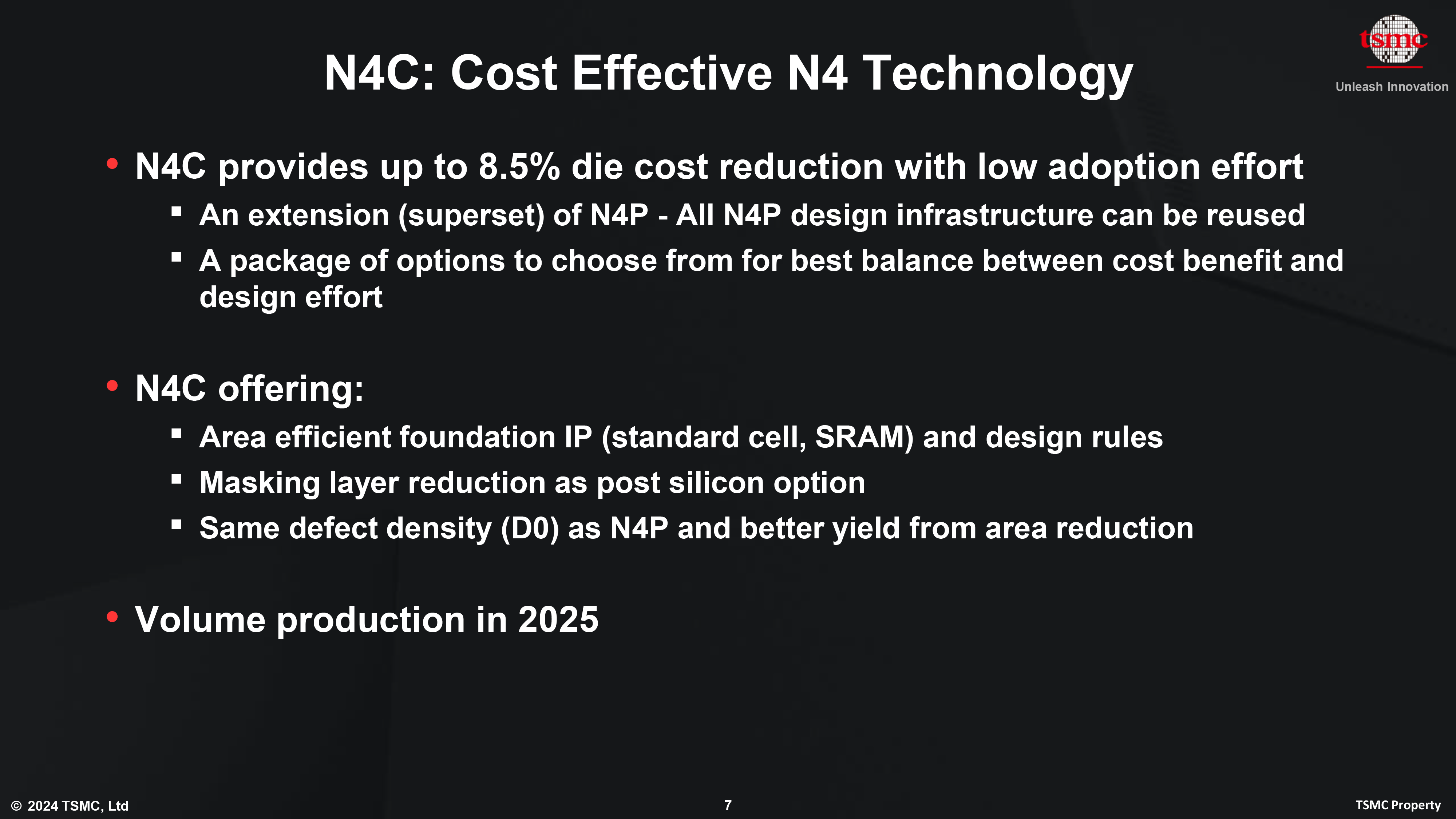
SSDs![TSMC Preps Cheaper 4nm N4C Process For 2025, Aiming For 8.5% Cost Reduction <p align="center"><a href="https://www.anandtech.com/show/21371/tsmc-preps-lower-cost-4nm-n4c-process-for-2025"><img src="https://images.anandtech.com/doci/21371/tsmc_semiconductor_fab12_1_678x452_575px.jpg" alt="" /></a></p><p><p>While the bulk of attention on TSMC is aimed at its leading-edge nodes, such as N3E and N2, loads of chips will continue to be made using more mature and proven process technologies for years to come. Which is why TSMC has continued to refine its existing nodes, including its current-generation 5nm-class offerings. To that end, at its North American Technology Symposium 2024, the company introduced a new, optimized 5nm-class node: N4C.</p>
<p>TSMC's N4C process belongs to the company's 5nm-class family of fab nodes and is a superset of N4P, the most advanced technology in that family. In a bid to further bring down 5nm manufacturing costs, for TSMC is implementing several changes for N4C, including rearchitecting their standard cell and SRAM cell, changing some design rules, and reducing the number of masking layers. As a result of these improvements, the company expects N4C to achieve both smaller die sizes as well as a reduction in production complexity, which in turn will bring die costs down by up to 8.5%. Furthermore, with the same wafer-level defect density rate as N4P, N4C stands to offer even higher functional yields thanks to its die area reduction.</p>
<p>"So, we are not done with our 5nm and 4nm [technologies]," said Kevin Zhang, Vice President of Business Development at TSMC. "From N5 to N4, we have achieved 4% density improvement optical shrink, and we continue to enhance the transistor performance. Now we bring in N4C to our 4 nm technology portfolio. N4C allows our customers to reduce their costs by remove some of the masks and to also improve on the original IP design like a standard cell and SRAM to further reduce the overall product level cost of ownership."</p>
<p style="text-align: center;"><a href="https://www.anandtech.com/show/21371/tsmc-preps-lower-cost-4nm-n4c-process-for-2025"><img alt="" src="https://images.anandtech.com/doci/21371/tsmc-n4c.png" style="width: 100%;" /></a></p>
<p>TSMC says that N4C can use the same design infrastructure as N4P, though it is unclear whether N5 and N4P IP can be re-used for N4C-based chips. Meanwhile, TSMC indicates that it offers various options for chipmakers to find the right balance between cost benefits and design effort, so companies interested in adopting a 4nm-class process technologies could well adopt N4C.</p>
<p>The development of N4C comes as many of TSMC's chip design customers are preparing to launch chips based on the company's final generation of FinFET process technology, the 3nm N3 series. While N3 is expected to be a successful family, the high costs of N3B have been an issue, and the generation is marked by diminishing performance and transistor density returns altogether. Consequently, N4C could well become a major, long-lived node at TSMC, serving as a good fit for customers who want to stick to a more cost-effective FinFET node.</p>
<p>"This is a very significant enhancement, we are working with our customer, basically to extract more value from their 4 nm investment," Zhang said.</p>
<p>TSMC expects to start volume production of N4C chips some time next year. And with TSMC having produced 5nm-class for nearly half a decade at that point, N4C should be able to hit the ground running in terms of volume and yields.</p>
<h3><strong>Related Reading</strong></h3>
<ul>
<li><a href="https://www.anandtech.com/show/21369/tsmcs-16nm-technology-announced-for-late-2026-a16-with-super-power-rail-bspdn">TSMC's 1.6nm Technology Announced for Late 2026: A16 with "Super Power Rail" Backside Power</a></li>
<li><a href="https://www.anandtech.com/show/21370/tsmc-2nm-update-n2-in-2025-n2p-loses-bspdn-nanoflex-optimizations">TSMC 2nm Update: N2 In 2025, N2P Loses Backside Power, and NanoFlex Brings Optimal Cells</a></li>
<li><a href="https://www.anandtech.com/show/21372/tsmcs-system-on-wafer-platform-goes-3d-cow-sow">TSMC's System-on-Wafer Platform Goes 3D: CoW-SoW Stacks Up the Chips</a></li>
<li><a href="https://www.anandtech.com/show/21373/tsmc-adds-silicon-photonics-coupe-roadmap-128tbps-on-package">TSMC Jumps Into Silicon Photonics, Lays Out Roadmap For 12.8 Tbps COUPE On-Package Interconnect</a></li>
</ul>
</p> Semiconductors](https://lh3.googleusercontent.com/blogger_img_proxy/AEn0k_tAC0LBiPcuIyhyc5gLa6JN90l65tc8HDJQRPgQUhXdS5Juw-G4Pmbg3bAP8U_YMLa4CXbf5M1umUmhAl6K6YqfBMr1X4--hNS5gS7pisRI0TERftFjt92lPiOJHtRYFLOIhycoG-2IZt_8IexHhsxyBXUZ5EWyTQ=w72-h72-p-k-no-nu)
While the bulk of attention on TSMC is aimed at its leading-edge nodes, such as N3E and N2, loads of chips will continue to be made using more mature and proven process technologies for years to come. Which is why TSMC has continued to refine its existing nodes, including its current-generation 5nm-class offerings. To that end, at its North American Technology Symposium 2024, the company introduced a new, optimized 5nm-class node: N4C.
TSMC's N4C process belongs to the company's 5nm-class family of fab nodes and is a superset of N4P, the most advanced technology in that family. In a bid to further bring down 5nm manufacturing costs, for TSMC is implementing several changes for N4C, including rearchitecting their standard cell and SRAM cell, changing some design rules, and reducing the number of masking layers. As a result of these improvements, the company expects N4C to achieve both smaller die sizes as well as a reduction in production complexity, which in turn will bring die costs down by up to 8.5%. Furthermore, with the same wafer-level defect density rate as N4P, N4C stands to offer even higher functional yields thanks to its die area reduction.
"So, we are not done with our 5nm and 4nm [technologies]," said Kevin Zhang, Vice President of Business Development at TSMC. "From N5 to N4, we have achieved 4% density improvement optical shrink, and we continue to enhance the transistor performance. Now we bring in N4C to our 4 nm technology portfolio. N4C allows our customers to reduce their costs by remove some of the masks and to also improve on the original IP design like a standard cell and SRAM to further reduce the overall product level cost of ownership."
TSMC says that N4C can use the same design infrastructure as N4P, though it is unclear whether N5 and N4P IP can be re-used for N4C-based chips. Meanwhile, TSMC indicates that it offers various options for chipmakers to find the right balance between cost benefits and design effort, so companies interested in adopting a 4nm-class process technologies could well adopt N4C.
The development of N4C comes as many of TSMC's chip design customers are preparing to launch chips based on the company's final generation of FinFET process technology, the 3nm N3 series. While N3 is expected to be a successful family, the high costs of N3B have been an issue, and the generation is marked by diminishing performance and transistor density returns altogether. Consequently, N4C could well become a major, long-lived node at TSMC, serving as a good fit for customers who want to stick to a more cost-effective FinFET node.
"This is a very significant enhancement, we are working with our customer, basically to extract more value from their 4 nm investment," Zhang said.
TSMC expects to start volume production of N4C chips some time next year. And with TSMC having produced 5nm-class for nearly half a decade at that point, N4C should be able to hit the ground running in terms of volume and yields.
Kioxia's booth at FMS 2024 was a busy one with multiple technology demonstrations keeping visitors occupied. A walk-through of the BiCS 8 manufacturing process was the first to grab my attention. Kioxia and Western Digital announced the sampling of BiCS 8 in March 2023. We had touched briefly upon its CMOS Bonded Array (CBA) scheme in our coverage of Kioxial's 2Tb QLC NAND device and coverage of Western Digital's 128 TB QLC enterprise SSD proof-of-concept demonstration. At Kioxia's booth, we got more insights.
Traditionally, fabrication of flash chips involved placement of the associate logic circuitry (CMOS process) around the periphery of the flash array. The process then moved on to putting the CMOS under the cell array, but the wafer development process was serialized with the CMOS logic getting fabricated first followed by the cell array on top. However, this has some challenges because the cell array requires a high-temperature processing step to ensure higher reliability that can be detrimental to the health of the CMOS logic. Thanks to recent advancements in wafer bonding techniques, the new CBA process allows the CMOS wafer and cell array wafer to be processed independently in parallel and then pieced together, as shown in the models above.
The BiCS 8 3D NAND incorporates 218 layers, compared to 112 layers in BiCS 5 and 162 layers in BiCS 6. The company decided to skip over BiCS 7 (or, rather, it was probably a short-lived generation meant as an internal test vehicle). The generation retains the four-plane charge trap structure of BiCS 6. In its TLC avatar, it is available as a 1 Tbit device. The QLC version is available in two capacities - 1 Tbit and 2 Tbit.
Kioxia also noted that while the number of layers (218) doesn't compare favorably with the latest layer counts from the competition, its lateral scaling / cell shrinkage has enabled it to be competitive in terms of bit density as well as operating speeds (3200 MT/s). For reference, the latest shipping NAND from Micron - the G9 - has 276 layers with a bit density in TLC mode of 21 Gbit/mm2, and operates at up to 3600 MT/s. However, its 232L NAND operates only up to 2400 MT/s and has a bit density of 14.6 Gbit/mm2.
It must be noted that the CBA hybrid bonding process has advantages over the current processes used by other vendors - including Micron's CMOS under array (CuA) and SK hynix's 4D PUC (periphery-under-chip) developed in the late 2010s. It is expected that other NAND vendors will also move eventually to some variant of the hybrid bonding scheme used by Kioxia.
Storage
SK hynix early in Friday announced that the company has finished the development of it's PCB01 PCIe Gen5 SSD, the company's forthcoming high-end SSD for OEMs. Based on the company's new Alistar platform, the PCB01 is designed to deliver chart-topping performance for client machines. And, as a sign of the times, SK hynix is positioning the PCB01 for AI PCs, looking to synergize with the overall industry interest in anything and everything AI.
The bare, OEM-focused drives have previously been shown off by SK hynix, and make no attempt to hide what's under the hood. The PCB01 relies on SK hynix's Alistar controller, which features a PCIe Gen5 x4 host interface on the front end and eight NAND channels on the back end, placing it solidly in the realm of high-end SSDs. Paired with the Alistar controller is the company's latest 238-layer TLC NAND (H25T1TD48C & H25T2TD88C), which offers a maximum transfer speed of 2400 MT/second. Being that this is a high-end client SSD, there's also a DRAM chip on board, though the company isn't disclosing its capacity.
As with other high-end PCIe 5.0 client SSDs, SK hynix is planning on hitting peak read speeds of up to 14GB/second on the drive, while peak sequential write speeds should top 12GB/second (with pSLC caching, of course) – performance figures well within the realm of possibility for an 8 channel drive. As for random performance, at Computex the company was telling attendees that the drives should be able to sustain 4K random read and write rates of 2 million IOPS, which is very high as well. The SSDs are also said to consume up to 30% less power than 'predecessors,' according to SK hynix, though the company didn't elaborate on that figure. Typically in the storage industry, energy figures are based on iso-performance (rather than peak performance) – essentially measuring energy efficiency per bit rather than toal power consumption – and that is likely the case here as well.
At least initially, SK Hynix plans to release its PCB01 in three capacities – 512 GB, 1 TB, and 2 TB. The company has previously disclosed that their 238L TLC NAND has a capacity of 512Gbit, so these are typical capacity figures for single-sided drives. And while the focus of the company's press release this week was on OEM drives, this is the same controller and NAND that is also going into the company's previously-teased retail Platinum P51 SSD, so this week's reveal offers a bit more detail into what to expect from that drive family as well.
Specs aside, Ahn Hyun, the Head of the N-S Committee at SK hynix, said that multiple global CPU providers for on-device AI PCs are seeking collaboration for the compatibility validation process, which is underway, so expect PCB01 drives inside PCs in this back-to-school and holiday seasons.
"We will work towards enhancing our leadership as the global top AI memory provider also in the NAND solution space by successfully completing the customer validation and mass production of PCB01, which will be in the limelight," Ahn Hyun said.
SSDs
While the bulk of attention on TSMC is aimed at its leading-edge nodes, such as N3E and N2, loads of chips will continue to be made using more mature and proven process technologies for years to come. Which is why TSMC has continued to refine its existing nodes, including its current-generation 5nm-class offerings. To that end, at its North American Technology Symposium 2024, the company introduced a new, optimized 5nm-class node: N4C.
TSMC's N4C process belongs to the company's 5nm-class family of fab nodes and is a superset of N4P, the most advanced technology in that family. In a bid to further bring down 5nm manufacturing costs, for TSMC is implementing several changes for N4C, including rearchitecting their standard cell and SRAM cell, changing some design rules, and reducing the number of masking layers. As a result of these improvements, the company expects N4C to achieve both smaller die sizes as well as a reduction in production complexity, which in turn will bring die costs down by up to 8.5%. Furthermore, with the same wafer-level defect density rate as N4P, N4C stands to offer even higher functional yields thanks to its die area reduction.
"So, we are not done with our 5nm and 4nm [technologies]," said Kevin Zhang, Vice President of Business Development at TSMC. "From N5 to N4, we have achieved 4% density improvement optical shrink, and we continue to enhance the transistor performance. Now we bring in N4C to our 4 nm technology portfolio. N4C allows our customers to reduce their costs by remove some of the masks and to also improve on the original IP design like a standard cell and SRAM to further reduce the overall product level cost of ownership."
TSMC says that N4C can use the same design infrastructure as N4P, though it is unclear whether N5 and N4P IP can be re-used for N4C-based chips. Meanwhile, TSMC indicates that it offers various options for chipmakers to find the right balance between cost benefits and design effort, so companies interested in adopting a 4nm-class process technologies could well adopt N4C.
The development of N4C comes as many of TSMC's chip design customers are preparing to launch chips based on the company's final generation of FinFET process technology, the 3nm N3 series. While N3 is expected to be a successful family, the high costs of N3B have been an issue, and the generation is marked by diminishing performance and transistor density returns altogether. Consequently, N4C could well become a major, long-lived node at TSMC, serving as a good fit for customers who want to stick to a more cost-effective FinFET node.
"This is a very significant enhancement, we are working with our customer, basically to extract more value from their 4 nm investment," Zhang said.
TSMC expects to start volume production of N4C chips some time next year. And with TSMC having produced 5nm-class for nearly half a decade at that point, N4C should be able to hit the ground running in terms of volume and yields.


When Western Digital introduced its Ultrastar DC SN861 SSDs earlier this year, the company did not disclose which controller it used for these drives, which made many observers presume that WD was using an in-house controller. But a recent teardown of the drive shows that is not the case; instead, the company is using a controller from Fadu, a South Korean company founded in 2015 that specializes on enterprise-grade turnkey SSD solutions.
The Western Digital Ultrastar DC SN861 SSD is aimed at performance-hungry hyperscale datacenters and enterprise customers which are adopting PCIe Gen5 storage devices these days. And, as uncovered in photos from a recent Storage Review article, the drive is based on Fadu's FC5161 NVMe 2.0-compliant controller. The FC5161 utilizes 16 NAND channels supporting an ONFi 5.0 2400 MT/s interface, and features a combination of enterprise-grade capabilities (OCP Cloud Spec 2.0, SR-IOV, up to 512 name spaces for ZNS support, flexible data placement, NVMe-MI 1.2, advanced security, telemetry, power loss protection) not available on other off-the-shelf controllers – or on any previous Western Digital controllers.
The Ultrastar DC SN861 SSD offers sequential read speeds up to 13.7 GB/s as well as sequential write speeds up to 7.5 GB/s. As for random performance, it boasts with an up to 3.3 million random 4K read IOPS and up to 0.8 million random 4K write IOPS. The drives are available in capacities between 1.6 TB and 7.68 TB with one or three drive writes per day (DWPD) over five years rating as well as in U.2 and E1.S form-factors.
While the two form factors of the SN861 share a similar technical design, Western Digital has tailored each version for distinct workloads: the E1.S supports FDP and performance enhancements specifically for cloud environments. By contrast, the U.2 model is geared towards high-performance enterprise tasks and emerging applications like AI.
Without any doubts, Western Digital's Ultrastar DC SN861 is a feature-rich high-performance enterprise-grade SSD. It has another distinctive feature: a 5W idle power consumption, which is rather low by the standards of enterprise-grade drives (e.g., it is 1W lower compared to the SN840). While the difference with predecessors may be just 1W, hyperscalers deploy thousands of drives and for their TCO every watt counts.
Western Digital's Ultrastar DC SN861 SSDs are now available for purchase to select customers (such as Meta) and to interested parties. Prices are unknown, but they will depend on such factors as volumes.
Sources: Fadu, Storage Review
Storage
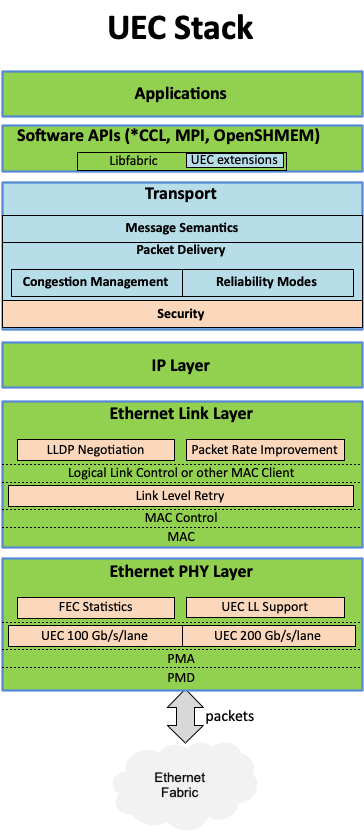
The Ultra Ethernet Consortium (UEC) has announced this week that the next-generation interconnection consortium has grown to 55 members. And as the group works towards developing the initial version of their ultra-fast Ethernet standard, they have released some of the first technical details on the upcoming standard.
Formed in the summer of 2023, the UEC aims to develop a new standard for interconnection for AI and HPC datacenter needs, serving as a de-facto (if not de-jure) alternative to InfiniBand, which is largely under the control of NVIDIA these days. The UEC began to accept new members back in November, and just in five months' time it gained 45 new members, which highlights massive interest for the new technology. The consortium now boasts 55 members and 715 industry experts, who are working across eight technical groups.
There is a lot of work at hand for the UEC, as the group has laid out in their latest development blog post, as the consortium works to to build a unified Ethernet-based communication stack for high-performance networking supporting artificial intelligence and high-performance computing clusters. The consortium's technical objectives include developing specifications, APIs, and source code for Ultra Ethernet communications, updating existing protocols, and introducing new mechanisms for telemetry, signaling, security, and congestion management. In particular, Ultra Ethernet introduces the UEC Transport (UET) for higher network utilization and lower tail latency to speed up RDMA (Remote Direct Memory Access) operation over Ethernet. Key features include multi-path packet spraying, flexible ordering, and advanced congestion control, ensuring efficient and reliable data transfer.
These enhancements are designed to address the needs of large AI and HPC clusters — with separate profiles for each type of deployment — though everything is done in a surgical manner to enhance the technology, but reuse as much of the existing Ethernet as possible to maintain cost efficiency and interoperability.
The consortium's founding members include AMD, Arista, Broadcom, Cisco, Eviden (an Atos Business), HPE, Intel, Meta, and Microsoft. After the Ultra Ethernet Consortium (UEC) began to accept new members in October, 2023, numerous industry heavyweights have joined the group, including Baidu, Dell, Huawei, IBM, Nokia, Lenovo, Supermicro, and Tencent.
The consortium currently plans to release the initial 1.0 version of the UEC specification publicly sometime in the third quarter of 2024.
"There was always a recognition that UEC was meeting a need in the industry," said J Metz, Chair of the UEC Steering Committee. "There is a strong desire to have an open, accessible, Ethernet-based network specifically designed to accommodate AI and HPC workload requirements. This level of involvement is encouraging; it helps us achieve the goal of broad interoperability and stability."
While it is evident that then Ultra Ethernet Consortium is gaining support across the industry, it is still unclear where other industry behemoths like AWS and Google stand. While the hardware companies involved can design Ultra Ethernet support into their hardware and systems, the technology ultimately exists to serve large datacenter and HPC system operators. So it will be interesting to see what interest they take in (and how quickly they adopt) the nascent Ethernet backbone technology once hardware incorporating it is ready.
Networking
![]()
In addition to revealing its roadmap and plans concerning its current leading-edge process technologies, TSMC also shared progress of its N2 node as part of its Symposiums 2024. The company's first 2nm-class fabrication node, and predominantly featuring gate-all-around transistors, according to TSMC N2 has almost achieved its target performance and yield goals, which places it on track to enter high-volume manufacturing in the second half of 2025.
TSMC states that 'N2 development is well on track and N2P is next.' In particular, gate-all-around nanosheet devices currently achieve over 90% of their expected performance, whereas yields of 256 Mb SRAM (32 MB) devices already exceeds 80%, depending on the batch. All of this for a node that is over a year away from mass production.
Meanwhile, average yield of a 256 Mb SRAM was around 70% as of March, 2024, up from around 35% in April, 2023. Device performance has also been improving with higher frequencies being achieved while keeping power consumption in check.
Chip designer interest towards TSMC's first 2nm-class gate-all-around nanosheet transistor-based technology is significant, too. The number of new tape-outs (NTOs) in the first year of N2 is over two-times higher than it was for N5. Though with that said, given TSMC's close working relationship with a handful of high-volume vendors – most notably Appe – NTOs can be a very misleading figure since the first year of a new node at TSMC is capacity constrained, and consequently the bulk of that capacity goes to TSMC's priority partners.
Meanwhile, there were considerably more N5 tapeouts in its second year (some where N5P, of course) and N2 promises to have 2.6X more NTOs in its second year. So the node indeed looks quite promising. In fact, based on TSMC's slides (which we're unfortunately not able to republish), N2 is more popular than N3 in terms of NTOs both in the first and the second years of existence.
When it comes to the second year of N2, in the second half of 2026 TSMC plans to roll out its N2P technology, which promises additional performance and power benefits. N2P is expected to improve frequency by 15% - 20%, reduce power consumption by 30% - 40%, and increase chip density by over 1.15 times compared to N3E, significant benefits to move to all-new GAA nanosheet transistors.
Finally, for those companies that need the best in performance, power, and density, TSMC is poised to offer their A16 process in 2026. That node will also bring in backside power delivery, which will add costs, but is expected to greatly improve performance efficiency and scaling.
Semiconductors
While the bulk of attention on TSMC is aimed at its leading-edge nodes, such as N3E and N2, loads of chips will continue to be made using more mature and proven process technologies for years to come. Which is why TSMC has continued to refine its existing nodes, including its current-generation 5nm-class offerings. To that end, at its North American Technology Symposium 2024, the company introduced a new, optimized 5nm-class node: N4C.
TSMC's N4C process belongs to the company's 5nm-class family of fab nodes and is a superset of N4P, the most advanced technology in that family. In a bid to further bring down 5nm manufacturing costs, for TSMC is implementing several changes for N4C, including rearchitecting their standard cell and SRAM cell, changing some design rules, and reducing the number of masking layers. As a result of these improvements, the company expects N4C to achieve both smaller die sizes as well as a reduction in production complexity, which in turn will bring die costs down by up to 8.5%. Furthermore, with the same wafer-level defect density rate as N4P, N4C stands to offer even higher functional yields thanks to its die area reduction.
"So, we are not done with our 5nm and 4nm [technologies]," said Kevin Zhang, Vice President of Business Development at TSMC. "From N5 to N4, we have achieved 4% density improvement optical shrink, and we continue to enhance the transistor performance. Now we bring in N4C to our 4 nm technology portfolio. N4C allows our customers to reduce their costs by remove some of the masks and to also improve on the original IP design like a standard cell and SRAM to further reduce the overall product level cost of ownership."
TSMC says that N4C can use the same design infrastructure as N4P, though it is unclear whether N5 and N4P IP can be re-used for N4C-based chips. Meanwhile, TSMC indicates that it offers various options for chipmakers to find the right balance between cost benefits and design effort, so companies interested in adopting a 4nm-class process technologies could well adopt N4C.
The development of N4C comes as many of TSMC's chip design customers are preparing to launch chips based on the company's final generation of FinFET process technology, the 3nm N3 series. While N3 is expected to be a successful family, the high costs of N3B have been an issue, and the generation is marked by diminishing performance and transistor density returns altogether. Consequently, N4C could well become a major, long-lived node at TSMC, serving as a good fit for customers who want to stick to a more cost-effective FinFET node.
"This is a very significant enhancement, we are working with our customer, basically to extract more value from their 4 nm investment," Zhang said.
TSMC expects to start volume production of N4C chips some time next year. And with TSMC having produced 5nm-class for nearly half a decade at that point, N4C should be able to hit the ground running in terms of volume and yields.

Lorem Ipsum is simply dummy text of the printing and typesetting industry. Lorem Ipsum has been the industry's.
Kioxia's booth at FMS 2024 was a busy one with multiple technology demonstrations keeping visitors occupied. A walk-through of the BiCS 8 manufacturing process was the first to grab my attention. Kioxia and Western Digital announced the sampling of BiCS 8 in March 2023. We had touched briefly upon its CMOS Bonded Array (CBA) scheme in our coverage of Kioxial's 2Tb QLC NAND device and coverage of Western Digital's 128 TB QLC enterprise SSD proof-of-concept demonstration. At Kioxia's booth, we got more insights.
Traditionally, fabrication of flash chips involved placement of the associate logic circuitry (CMOS process) around the periphery of the flash array. The process then moved on to putting the CMOS under the cell array, but the wafer development process was serialized with the CMOS logic getting fabricated first followed by the cell array on top. However, this has some challenges because the cell array requires a high-temperature processing step to ensure higher reliability that can be detrimental to the health of the CMOS logic. Thanks to recent advancements in wafer bonding techniques, the new CBA process allows the CMOS wafer and cell array wafer to be processed independently in parallel and then pieced together, as shown in the models above.
The BiCS 8 3D NAND incorporates 218 layers, compared to 112 layers in BiCS 5 and 162 layers in BiCS 6. The company decided to skip over BiCS 7 (or, rather, it was probably a short-lived generation meant as an internal test vehicle). The generation retains the four-plane charge trap structure of BiCS 6. In its TLC avatar, it is available as a 1 Tbit device. The QLC version is available in two capacities - 1 Tbit and 2 Tbit.
Kioxia also noted that while the number of layers (218) doesn't compare favorably with the latest layer counts from the competition, its lateral scaling / cell shrinkage has enabled it to be competitive in terms of bit density as well as operating speeds (3200 MT/s). For reference, the latest shipping NAND from Micron - the G9 - has 276 layers with a bit density in TLC mode of 21 Gbit/mm2, and operates at up to 3600 MT/s. However, its 232L NAND operates only up to 2400 MT/s and has a bit density of 14.6 Gbit/mm2.
It must be noted that the CBA hybrid bonding process has advantages over the current processes used by other vendors - including Micron's CMOS under array (CuA) and SK hynix's 4D PUC (periphery-under-chip) developed in the late 2010s. It is expected that other NAND vendors will also move eventually to some variant of the hybrid bonding scheme used by Kioxia.
Storage
SK hynix early in Friday announced that the company has finished the development of it's PCB01 PCIe Gen5 SSD, the company's forthcoming high-end SSD for OEMs. Based on the company's new Alistar platform, the PCB01 is designed to deliver chart-topping performance for client machines. And, as a sign of the times, SK hynix is positioning the PCB01 for AI PCs, looking to synergize with the overall industry interest in anything and everything AI.
The bare, OEM-focused drives have previously been shown off by SK hynix, and make no attempt to hide what's under the hood. The PCB01 relies on SK hynix's Alistar controller, which features a PCIe Gen5 x4 host interface on the front end and eight NAND channels on the back end, placing it solidly in the realm of high-end SSDs. Paired with the Alistar controller is the company's latest 238-layer TLC NAND (H25T1TD48C & H25T2TD88C), which offers a maximum transfer speed of 2400 MT/second. Being that this is a high-end client SSD, there's also a DRAM chip on board, though the company isn't disclosing its capacity.
As with other high-end PCIe 5.0 client SSDs, SK hynix is planning on hitting peak read speeds of up to 14GB/second on the drive, while peak sequential write speeds should top 12GB/second (with pSLC caching, of course) – performance figures well within the realm of possibility for an 8 channel drive. As for random performance, at Computex the company was telling attendees that the drives should be able to sustain 4K random read and write rates of 2 million IOPS, which is very high as well. The SSDs are also said to consume up to 30% less power than 'predecessors,' according to SK hynix, though the company didn't elaborate on that figure. Typically in the storage industry, energy figures are based on iso-performance (rather than peak performance) – essentially measuring energy efficiency per bit rather than toal power consumption – and that is likely the case here as well.
At least initially, SK Hynix plans to release its PCB01 in three capacities – 512 GB, 1 TB, and 2 TB. The company has previously disclosed that their 238L TLC NAND has a capacity of 512Gbit, so these are typical capacity figures for single-sided drives. And while the focus of the company's press release this week was on OEM drives, this is the same controller and NAND that is also going into the company's previously-teased retail Platinum P51 SSD, so this week's reveal offers a bit more detail into what to expect from that drive family as well.
Specs aside, Ahn Hyun, the Head of the N-S Committee at SK hynix, said that multiple global CPU providers for on-device AI PCs are seeking collaboration for the compatibility validation process, which is underway, so expect PCB01 drives inside PCs in this back-to-school and holiday seasons.
"We will work towards enhancing our leadership as the global top AI memory provider also in the NAND solution space by successfully completing the customer validation and mass production of PCB01, which will be in the limelight," Ahn Hyun said.
SSDs

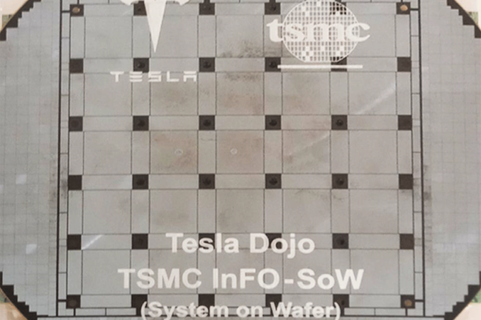
![TSMC's System-on-Wafer Platform Goes 3D: CoW-SoW Stacks Up the Chips <p align="center"><a href="https://www.anandtech.com/show/21372/tsmcs-system-on-wafer-platform-goes-3d-cow-sow"><img src="https://images.anandtech.com/doci/21372/tsmc-sow-tesla-dojo-678_575px.png" alt="" /></a></p><p><p>TSMC has been offering its System-on-Wafer integration technology, InFO-SoW, since 2020. For now, only Cerebras and Tesla have developed wafer scale processor designs using it, as while they have fantastic performance and power efficiency, wafer-scale processors are extremely complex to develop and produce. But TSMC believes that not only will wafer-scale designs ramp up in usage, but that megatrends like AI and HPC will call for even more complex solutions: vertically stacked system-on-wafer designs.</p>
<p style="text-align: center;"><a href="https://www.anandtech.com/show/21372/tsmcs-system-on-wafer-platform-goes-3d-cow-sow"><img alt="" src="https://images.anandtech.com/doci/21372/tsmc-sow-tesla-dojo-575px.png" /></a></p>
<p>Tesla Dojo's wafer-scale processors — the first solutions based based on TSMC's InFO-SoW technology that are in mass production — have a number of benefits over typical system-in-packages (SiPs), including low-latency high-bandwidth core-to-core communications, very high performance and bandwidth density, relatively low power delivery network impendance, high performance efficiency, and redunancy.</p>
<p>But with InFO-SoW and other wafer scale integration methods, processor designers have to rely solely on on-chip memory. This is perfectly adequate for many applications, but it may not be enough for next-generation AI workloads. Furthermore, with InFO-SoW, the whole wafer has to be processed using one fabrication technology, which may not be optimal, or too expensive for certain designs.</p>
<p style="text-align: center;"><a href="https://www.anandtech.com/show/21372/tsmcs-system-on-wafer-platform-goes-3d-cow-sow"><img alt="" src="https://images.anandtech.com/doci/21372/tsmc-sow-cowos-evolution-575px.png" /></a></p>
<p>So, with its next-generation system-on-wafer platform, TSMC plans to bring together two of its packaging technologies: InFO-SoW and System on Integrated Chips (SoIC), which will allow it to stack memory or logic on top of a system-on-wafer using its Chip-on-Wafer (CoW) method. The CoW-SoW technology, which the company announced at its North American Technology Symposium, will be ready for mass production in 2027.</p>
<p>For now, TSMC is mostly talking about wedding wafer scale processors with HBM4 memory. And given that HBM4 stacks will feature a 2048-bit interface, its tighter integration with logic is something that the industry is considering.</p>
<p>"So, in the future, using wafer level integrations [will allow] our customers to integrate even more logic and memory together," said Kevin Zhang, Vice President of Business Development at TSMC. "SoW is no longer a fiction, this is something we already work with our customers [on] to produce some of the products already in place. This we think by leveraging our advanced wafer level integration technology, we can provide our customer a very important the path allow them to continue to grow their capability to bring in more computation, more energy efficient computation, to their AI cluster or [supercomputer]."</p>
<h3><strong>Related Reading</strong></h3>
<ul>
<li><a href="https://www.anandtech.com/show/21369/tsmcs-16nm-technology-announced-for-late-2026-a16-with-super-power-rail-bspdn">TSMC's 1.6nm Technology Announced for Late 2026: A16 with "Super Power Rail" Backside Power</a></li>
<li><a href="https://www.anandtech.com/show/21370/tsmc-2nm-update-n2-in-2025-n2p-loses-bspdn-nanoflex-optimizations">TSMC 2nm Update: N2 In 2025, N2P Loses Backside Power, and NanoFlex Brings Optimal Cells</a></li>
<li><a href="https://www.anandtech.com/show/21371/tsmc-preps-lower-cost-4nm-n4c-process-for-2025">TSMC Preps Cheaper 4nm N4C Process For 2025, Aiming For 8.5% Cost Reduction</a></li>
</ul>
</p> Semiconductors](https://lh3.googleusercontent.com/blogger_img_proxy/AEn0k_vh6xTbtabBxMA8qM45k8gscbQMtg42B7WldZylA3gvegyNKoLsg0F9hpw2hdTou0Fv3umKtzicYy3duIZT8Ey4JXZ4YbsB4fJgmX_Z41bNsltUgAfLLc3QMZ6fUOV0vbWXfqNVyYsfPSpRe9s=w72-h72-p-k-no-nu)


, which offers a maximum transfer speed of 2400 MT/second. Being that this is a high-end client SSD, there's also a DRAM chip on board, though the company isn't disclosing its capacity.</p>
<p style="text-align: center;"><a href="https://www.anandtech.com/show/21460/sk-hynix-wraps-up-dev-on-high-end-pcie-5-pcb01-oem-ssd"><img alt="" src="https://images.anandtech.com/doci/21460/IMG_1305_575px.jpg" /></a></p>
<p>As with other high-end PCIe 5.0 client SSDs, SK hynix is planning on hitting peak read speeds of up to 14GB/second on the drive, while peak sequential write speeds should top 12GB/second (with pSLC caching, of course) – performance figures well within the realm of possibility for an 8 channel drive. As for random performance, at Computex the company was telling attendees that the drives should be able to sustain 4K random read and write rates of 2 million IOPS, which is very high as well. The SSDs are also said to consume up to 30% less power than 'predecessors,' according to SK hynix, though the company didn't elaborate on that figure. Typically in the storage industry, energy figures are based on iso-performance (rather than peak performance) – essentially measuring energy efficiency per bit rather than toal power consumption – and that is likely the case here as well.</p>
<p style="text-align: center;"><a href="https://www.anandtech.com/show/21460/sk-hynix-wraps-up-dev-on-high-end-pcie-5-pcb01-oem-ssd"><img alt="" src="https://images.anandtech.com/doci/21460/IMG_1304_575px.jpg" /></a></p>
<p>At least initially, SK Hynix plans to release its PCB01 in three capacities – 512 GB, 1 TB, and 2 TB. The company has previously disclosed that their 238L TLC NAND has a capacity of 512Gbit, so these are typical capacity figures for single-sided drives. And while the focus of the company's press release this week was on OEM drives, this is the same controller and NAND that is also going into the company's <a href="https://www.anandtech.com/show/21313/sk-hynix-platinum-p51-gen5-ssd-with-238l-nand-spotted-at-gtc">previously-teased retail Platinum P51 SSD</a>, so this week's reveal offers a bit more detail into what to expect from that drive family as well.</p>
<p>Specs aside, Ahn Hyun, the Head of the N-S Committee at SK hynix, said that multiple global CPU providers for on-device AI PCs are seeking collaboration for the compatibility validation process, which is underway, so expect PCB01 drives inside PCs in this back-to-school and holiday seasons.</p>
<p>"We will work towards enhancing our leadership as the global top AI memory provider also in the NAND solution space by successfully completing the customer validation and mass production of PCB01, which will be in the limelight," Ahn Hyun said.</p>
</p> SSDs)
, which offers a maximum transfer speed of 2400 MT/second. Being that this is a high-end client SSD, there's also a DRAM chip on board, though the company isn't disclosing its capacity.</p>
<p style="text-align: center;"><a href="https://www.anandtech.com/show/21460/sk-hynix-wraps-up-dev-on-high-end-pcie-5-pcb01-oem-ssd"><img alt="" src="https://images.anandtech.com/doci/21460/IMG_1305_575px.jpg" /></a></p>
<p>As with other high-end PCIe 5.0 client SSDs, SK hynix is planning on hitting peak read speeds of up to 14GB/second on the drive, while peak sequential write speeds should top 12GB/second (with pSLC caching, of course) – performance figures well within the realm of possibility for an 8 channel drive. As for random performance, at Computex the company was telling attendees that the drives should be able to sustain 4K random read and write rates of 2 million IOPS, which is very high as well. The SSDs are also said to consume up to 30% less power than 'predecessors,' according to SK hynix, though the company didn't elaborate on that figure. Typically in the storage industry, energy figures are based on iso-performance (rather than peak performance) – essentially measuring energy efficiency per bit rather than toal power consumption – and that is likely the case here as well.</p>
<p style="text-align: center;"><a href="https://www.anandtech.com/show/21460/sk-hynix-wraps-up-dev-on-high-end-pcie-5-pcb01-oem-ssd"><img alt="" src="https://images.anandtech.com/doci/21460/IMG_1304_575px.jpg" /></a></p>
<p>At least initially, SK Hynix plans to release its PCB01 in three capacities – 512 GB, 1 TB, and 2 TB. The company has previously disclosed that their 238L TLC NAND has a capacity of 512Gbit, so these are typical capacity figures for single-sided drives. And while the focus of the company's press release this week was on OEM drives, this is the same controller and NAND that is also going into the company's <a href="https://www.anandtech.com/show/21313/sk-hynix-platinum-p51-gen5-ssd-with-238l-nand-spotted-at-gtc">previously-teased retail Platinum P51 SSD</a>, so this week's reveal offers a bit more detail into what to expect from that drive family as well.</p>
<p>Specs aside, Ahn Hyun, the Head of the N-S Committee at SK hynix, said that multiple global CPU providers for on-device AI PCs are seeking collaboration for the compatibility validation process, which is underway, so expect PCB01 drives inside PCs in this back-to-school and holiday seasons.</p>
<p>"We will work towards enhancing our leadership as the global top AI memory provider also in the NAND solution space by successfully completing the customer validation and mass production of PCB01, which will be in the limelight," Ahn Hyun said.</p>
</p> SSDs | https://compbuddey.blogspot.com/2024/07/sk-hynix-wraps-up-dev-work-on-high-end.html)
, which offers a maximum transfer speed of 2400 MT/second. Being that this is a high-end client SSD, there's also a DRAM chip on board, though the company isn't disclosing its capacity.</p>
<p style="text-align: center;"><a href="https://www.anandtech.com/show/21460/sk-hynix-wraps-up-dev-on-high-end-pcie-5-pcb01-oem-ssd"><img alt="" src="https://images.anandtech.com/doci/21460/IMG_1305_575px.jpg" /></a></p>
<p>As with other high-end PCIe 5.0 client SSDs, SK hynix is planning on hitting peak read speeds of up to 14GB/second on the drive, while peak sequential write speeds should top 12GB/second (with pSLC caching, of course) – performance figures well within the realm of possibility for an 8 channel drive. As for random performance, at Computex the company was telling attendees that the drives should be able to sustain 4K random read and write rates of 2 million IOPS, which is very high as well. The SSDs are also said to consume up to 30% less power than 'predecessors,' according to SK hynix, though the company didn't elaborate on that figure. Typically in the storage industry, energy figures are based on iso-performance (rather than peak performance) – essentially measuring energy efficiency per bit rather than toal power consumption – and that is likely the case here as well.</p>
<p style="text-align: center;"><a href="https://www.anandtech.com/show/21460/sk-hynix-wraps-up-dev-on-high-end-pcie-5-pcb01-oem-ssd"><img alt="" src="https://images.anandtech.com/doci/21460/IMG_1304_575px.jpg" /></a></p>
<p>At least initially, SK Hynix plans to release its PCB01 in three capacities – 512 GB, 1 TB, and 2 TB. The company has previously disclosed that their 238L TLC NAND has a capacity of 512Gbit, so these are typical capacity figures for single-sided drives. And while the focus of the company's press release this week was on OEM drives, this is the same controller and NAND that is also going into the company's <a href="https://www.anandtech.com/show/21313/sk-hynix-platinum-p51-gen5-ssd-with-238l-nand-spotted-at-gtc">previously-teased retail Platinum P51 SSD</a>, so this week's reveal offers a bit more detail into what to expect from that drive family as well.</p>
<p>Specs aside, Ahn Hyun, the Head of the N-S Committee at SK hynix, said that multiple global CPU providers for on-device AI PCs are seeking collaboration for the compatibility validation process, which is underway, so expect PCB01 drives inside PCs in this back-to-school and holiday seasons.</p>
<p>"We will work towards enhancing our leadership as the global top AI memory provider also in the NAND solution space by successfully completing the customer validation and mass production of PCB01, which will be in the limelight," Ahn Hyun said.</p>
</p> SSDs&body=https://compbuddey.blogspot.com/2024/07/sk-hynix-wraps-up-dev-work-on-high-end.html)
0 Comments