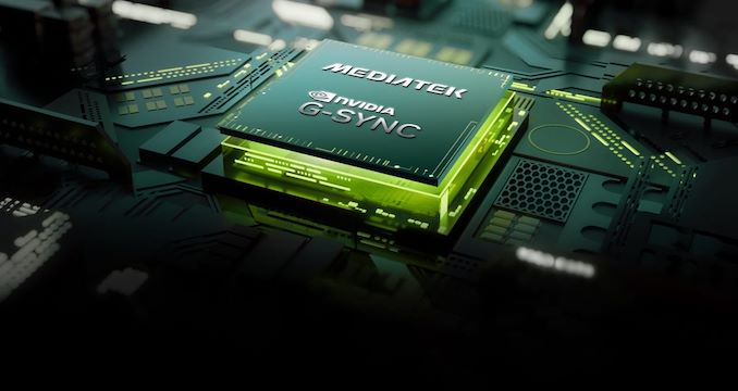

NVIDIA on Tuesday said that future monitor scalers from MediaTek will support its G-Sync technologies. NVIDIA is partnering with MediaTek to integrate its full range of G-Sync technologies into future monitors without requiring a standalone G-Sync module, which makes advanced gaming features more accessible across a broader range of displays.
Traditionally, G-Sync technology relied on a dedicated G-sync module – based on an Altera FPGA – to handle syncing display refresh rates with the GPU in order to reduce screen tearing, stutter, and input lag. As a more basic solution, in 2019 NVIDIA introduced G-Sync Compatible certification and branding, which leveraged the industry-standard VESA AdaptiveSync technology to handle variable refresh rates. In lieu of using a dedicated module, leveraging AdaptiveSync allowed for cheaper monitors, with NVIDIA's program serving as a stamp of approval that the monitor worked with NVIDIA GPUs and met NVIDIA's performance requirements. Still, G-Sync Compatible monitors still lack some features that, to date, require the dedicated G-Sync module.
Through this new partnership with MediaTek, MediaTek will bring support for all of NVIDIA's G-Sync technologies, including the latest G-Sync Pulsar, directly into their scalers. G-Sync Pulsar enhances motion clarity and reduces ghosting, providing a smoother gaming experience. In addition to variable refresh rates and Pulsar, MediaTek-based G-Sync displays will support such features as variable overdrive, 12-bit color, Ultra Low Motion Blur, low latency HDR, and Reflex Analyzer. This integration will allow more monitors to support a full range of G-Sync features without having to incorporate an expensive FPGA.
The first monitors to feature full G-Sync support without needing an NVIDIA module include the AOC Agon Pro AG276QSG2, Acer Predator XB273U F5, and ASUS ROG Swift 360Hz PG27AQNR. These monitors offer 360Hz refresh rates, 1440p resolution, and HDR support.
What remains to be seen is which specific MediaTek's scalers will support NVIDIA's G-Sync technology – or if the company is going to implement support into all of their scalers going forward. It also remains to be seen whether monitors with NVIDIA's dedicated G-Sync modules retain any advantages over displays with MediaTek's scalers.
Monitors

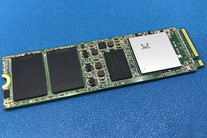
While Realtek is best known in the enthusiast space for for its peripheral controllers such as audio codecs and network controllers, the company also has a small-but-respectable SSD controller business that tends to fly under the radar due to its focus on entry-level and mainstream drives. But Realtek's stature in the SSD space is on the rise, as the company is not only planning new PCIe Gen5 SSD controllers, but also their first high-end, DRAM-equipped SSD controller.
For this year's Computex trade show, Realtek laid out a new SSD controller roadmap that calls for the company to release a trio of new SSD controllers over the next couple of years. First up is a new four-channel entry-level PCIe 4.0 controller, the RTS5776DL, which will be joined a bit later by a PCIe 5.0 variant, the RTS5781DL. But most interesting on Realtek's new roadmap is the final chip being planned: the eight-channel, DRAM-equipped RTS5782, which would be the company's first high-end SSD controller, capable of hitting sequential read rates as high as 14GB/second.
| Realtek NVMe SSD Controller Comparison | |||||||||
| RTS5782 | RTS5781DL | RTS5776DL | RTS5772DL | RTS5766DL | |||||
| Market Segment | High-End | Mainstream | Entry-Level | ||||||
| Error Correction | 4K LDPC | 2K LDPC | |||||||
| DRAM | DDR4, LPDDR4(X) | No | No | No | No | ||||
| Host Interface | PCIe 5.0 x4 | PCIe 5.0 x4 | PCIe 4.0 x4 | PCIe 4.0 x4 | PCIe 3.0 x4 | ||||
| NVMe Version | NVMe 2.0 | NVMe 2.0 | NVMe 2.0 | NVMe 1.4 | NVMe 1.4 | ||||
| NAND Channels, Interface Speed | 8 ch, 3600 MT/s |
4 ch, 3600 MT/s |
4 ch, 3600 MT/s |
8 ch, 1600 MT/s |
4 ch, 1200 MT/s |
||||
| Sequential Read | 14 GB/s | 10 GB/s | 7.4 GB/s | 6 GB/s | 3.2 GB/s | ||||
| Sequential Write | 12 GB/s | 10 GB/s | 7.4 GB/s | 6 GB/s | 2.2 GB/s | ||||
| 4KB Random Read IOPS | 2500k | 1400k | 1200k | - | - | ||||
| 4KB Random Write IOPS | 2500k | 1400k | 1200k | - | - | ||||
Diving a bit deeper into Realtek's roadmap, the RTS5776DL is traditional DRAM-less PCIe Gen4 x4 controller with four NAND chann... SSDs

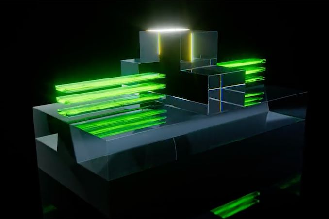
In addition to revealing its roadmap and plans concerning its current leading-edge process technologies, TSMC also shared progress of its N2 node as part of its Symposiums 2024. The company's first 2nm-class fabrication node, and predominantly featuring gate-all-around transistors, according to TSMC N2 has almost achieved its target performance and yield goals, which places it on track to enter high-volume manufacturing in the second half of 2025.
TSMC states that 'N2 development is well on track and N2P is next.' In particular, gate-all-around nanosheet devices currently achieve over 90% of their expected performance, whereas yields of 256 Mb SRAM (32 MB) devices already exceeds 80%, depending on the batch. All of this for a node that is over a year away from mass production.
Meanwhile, average yield of a 256 Mb SRAM was around 70% as of March, 2024, up from around 35% in April, 2023. Device performance has also been improving with higher frequencies being achieved while keeping power consumption in check.
Chip designer interest towards TSMC's first 2nm-class gate-all-around nanosheet transistor-based technology is significant, too. The number of new tape-outs (NTOs) in the first year of N2 is over two-times higher than it was for N5. Though with that said, given TSMC's close working relationship with a handful of high-volume vendors – most notably Appe – NTOs can be a very misleading figure since the first year of a new node at TSMC is capacity constrained, and consequently the bulk of that capacity goes to TSMC's priority partners.
Meanwhile, there were considerably more N5 tapeouts in its second year (some where N5P, of course) and N2 promises to have 2.6X more NTOs in its second year. So the node indeed looks quite promising. In fact, based on TSMC's slides (which we're unfortunately not able to republish), N2 is more popular than N3 in terms of NTOs both in the first and the second years of existence.
When it comes to the second year of N2, in the second half of 2026 TSMC plans to roll out its N2P technology, which promises additional performance and power benefits. N2P is expected to improve frequency by 15% - 20%, reduce power consumption by 30% - 40%, and increase chip density by over 1.15 times compared to N3E, significant benefits to move to all-new GAA nanosheet transistors.
Finally, for those companies that need the best in performance, power, and density, TSMC is poised to offer their A16 process in 2026. That node will also bring in backside power delivery, which will add costs, but is expected to greatly improve performance efficiency and scaling.
Semiconductors
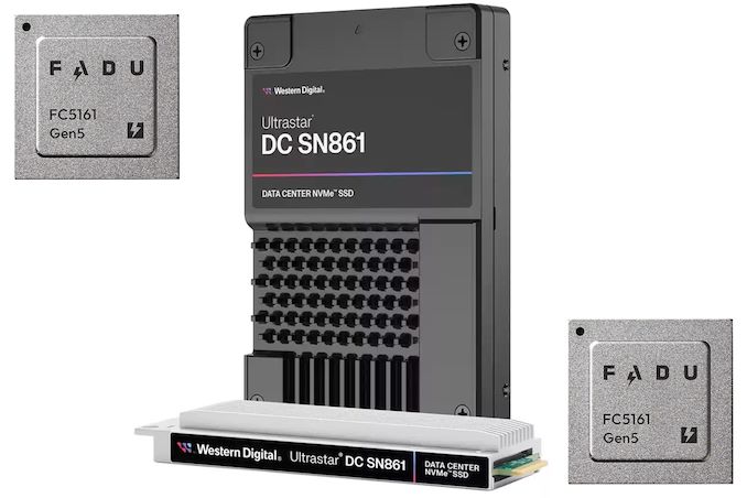
When Western Digital introduced its Ultrastar DC SN861 SSDs earlier this year, the company did not disclose which controller it used for these drives, which made many observers presume that WD was using an in-house controller. But a recent teardown of the drive shows that is not the case; instead, the company is using a controller from Fadu, a South Korean company founded in 2015 that specializes on enterprise-grade turnkey SSD solutions.
The Western Digital Ultrastar DC SN861 SSD is aimed at performance-hungry hyperscale datacenters and enterprise customers which are adopting PCIe Gen5 storage devices these days. And, as uncovered in photos from a recent Storage Review article, the drive is based on Fadu's FC5161 NVMe 2.0-compliant controller. The FC5161 utilizes 16 NAND channels supporting an ONFi 5.0 2400 MT/s interface, and features a combination of enterprise-grade capabilities (OCP Cloud Spec 2.0, SR-IOV, up to 512 name spaces for ZNS support, flexible data placement, NVMe-MI 1.2, advanced security, telemetry, power loss protection) not available on other off-the-shelf controllers – or on any previous Western Digital controllers.
The Ultrastar DC SN861 SSD offers sequential read speeds up to 13.7 GB/s as well as sequential write speeds up to 7.5 GB/s. As for random performance, it boasts with an up to 3.3 million random 4K read IOPS and up to 0.8 million random 4K write IOPS. The drives are available in capacities between 1.6 TB and 7.68 TB with one or three drive writes per day (DWPD) over five years rating as well as in U.2 and E1.S form-factors.
While the two form factors of the SN861 share a similar technical design, Western Digital has tailored each version for distinct workloads: the E1.S supports FDP and performance enhancements specifically for cloud environments. By contrast, the U.2 model is geared towards high-performance enterprise tasks and emerging applications like AI.
Without any doubts, Western Digital's Ultrastar DC SN861 is a feature-rich high-performance enterprise-grade SSD. It has another distinctive feature: a 5W idle power consumption, which is rather low by the standards of enterprise-grade drives (e.g., it is 1W lower compared to the SN840). While the difference with predecessors may be just 1W, hyperscalers deploy thousands of drives and for their TCO every watt counts.
Western Digital's Ultrastar DC SN861 SSDs are now available for purchase to select customers (such as Meta) and to interested parties. Prices are unknown, but they will depend on such factors as volumes.
Sources: Fadu, Storage Review
Storage
While Realtek is best known in the enthusiast space for for its peripheral controllers such as audio codecs and network controllers, the company also has a small-but-respectable SSD controller business that tends to fly under the radar due to its focus on entry-level and mainstream drives. But Realtek's stature in the SSD space is on the rise, as the company is not only planning new PCIe Gen5 SSD controllers, but also their first high-end, DRAM-equipped SSD controller.
For this year's Computex trade show, Realtek laid out a new SSD controller roadmap that calls for the company to release a trio of new SSD controllers over the next couple of years. First up is a new four-channel entry-level PCIe 4.0 controller, the RTS5776DL, which will be joined a bit later by a PCIe 5.0 variant, the RTS5781DL. But most interesting on Realtek's new roadmap is the final chip being planned: the eight-channel, DRAM-equipped RTS5782, which would be the company's first high-end SSD controller, capable of hitting sequential read rates as high as 14GB/second.
| Realtek NVMe SSD Controller Comparison | |||||||||
| RTS5782 | RTS5781DL | RTS5776DL | RTS5772DL | RTS5766DL | |||||
| Market Segment | High-End | Mainstream | Entry-Level | ||||||
| Error Correction | 4K LDPC | 2K LDPC | |||||||
| DRAM | DDR4, LPDDR4(X) | No | No | No | No | ||||
| Host Interface | PCIe 5.0 x4 | PCIe 5.0 x4 | PCIe 4.0 x4 | PCIe 4.0 x4 | PCIe 3.0 x4 | ||||
| NVMe Version | NVMe 2.0 | NVMe 2.0 | NVMe 2.0 | NVMe 1.4 | NVMe 1.4 | ||||
| NAND Channels, Interface Speed | 8 ch, 3600 MT/s |
4 ch, 3600 MT/s |
4 ch, 3600 MT/s |
8 ch, 1600 MT/s |
4 ch, 1200 MT/s |
||||
| Sequential Read | 14 GB/s | 10 GB/s | 7.4 GB/s | 6 GB/s | 3.2 GB/s | ||||
| Sequential Write | 12 GB/s | 10 GB/s | 7.4 GB/s | 6 GB/s | 2.2 GB/s | ||||
| 4KB Random Read IOPS | 2500k | 1400k | 1200k | - | - | ||||
| 4KB Random Write IOPS | 2500k | 1400k | 1200k | - | - | ||||
Diving a bit deeper into Realtek's roadmap, the RTS5776DL is traditional DRAM-less PCIe Gen4 x4 controller with four NAND chann... SSDs
In addition to revealing its roadmap and plans concerning its current leading-edge process technologies, TSMC also shared progress of its N2 node as part of its Symposiums 2024. The company's first 2nm-class fabrication node, and predominantly featuring gate-all-around transistors, according to TSMC N2 has almost achieved its target performance and yield goals, which places it on track to enter high-volume manufacturing in the second half of 2025.
TSMC states that 'N2 development is well on track and N2P is next.' In particular, gate-all-around nanosheet devices currently achieve over 90% of their expected performance, whereas yields of 256 Mb SRAM (32 MB) devices already exceeds 80%, depending on the batch. All of this for a node that is over a year away from mass production.
Meanwhile, average yield of a 256 Mb SRAM was around 70% as of March, 2024, up from around 35% in April, 2023. Device performance has also been improving with higher frequencies being achieved while keeping power consumption in check.
Chip designer interest towards TSMC's first 2nm-class gate-all-around nanosheet transistor-based technology is significant, too. The number of new tape-outs (NTOs) in the first year of N2 is over two-times higher than it was for N5. Though with that said, given TSMC's close working relationship with a handful of high-volume vendors – most notably Appe – NTOs can be a very misleading figure since the first year of a new node at TSMC is capacity constrained, and consequently the bulk of that capacity goes to TSMC's priority partners.
Meanwhile, there were considerably more N5 tapeouts in its second year (some where N5P, of course) and N2 promises to have 2.6X more NTOs in its second year. So the node indeed looks quite promising. In fact, based on TSMC's slides (which we're unfortunately not able to republish), N2 is more popular than N3 in terms of NTOs both in the first and the second years of existence.
When it comes to the second year of N2, in the second half of 2026 TSMC plans to roll out its N2P technology, which promises additional performance and power benefits. N2P is expected to improve frequency by 15% - 20%, reduce power consumption by 30% - 40%, and increase chip density by over 1.15 times compared to N3E, significant benefits to move to all-new GAA nanosheet transistors.
Finally, for those companies that need the best in performance, power, and density, TSMC is poised to offer their A16 process in 2026. That node will also bring in backside power delivery, which will add costs, but is expected to greatly improve performance efficiency and scaling.
Semiconductors
When Western Digital introduced its Ultrastar DC SN861 SSDs earlier this year, the company did not disclose which controller it used for these drives, which made many observers presume that WD was using an in-house controller. But a recent teardown of the drive shows that is not the case; instead, the company is using a controller from Fadu, a South Korean company founded in 2015 that specializes on enterprise-grade turnkey SSD solutions.
The Western Digital Ultrastar DC SN861 SSD is aimed at performance-hungry hyperscale datacenters and enterprise customers which are adopting PCIe Gen5 storage devices these days. And, as uncovered in photos from a recent Storage Review article, the drive is based on Fadu's FC5161 NVMe 2.0-compliant controller. The FC5161 utilizes 16 NAND channels supporting an ONFi 5.0 2400 MT/s interface, and features a combination of enterprise-grade capabilities (OCP Cloud Spec 2.0, SR-IOV, up to 512 name spaces for ZNS support, flexible data placement, NVMe-MI 1.2, advanced security, telemetry, power loss protection) not available on other off-the-shelf controllers – or on any previous Western Digital controllers.
The Ultrastar DC SN861 SSD offers sequential read speeds up to 13.7 GB/s as well as sequential write speeds up to 7.5 GB/s. As for random performance, it boasts with an up to 3.3 million random 4K read IOPS and up to 0.8 million random 4K write IOPS. The drives are available in capacities between 1.6 TB and 7.68 TB with one or three drive writes per day (DWPD) over five years rating as well as in U.2 and E1.S form-factors.
While the two form factors of the SN861 share a similar technical design, Western Digital has tailored each version for distinct workloads: the E1.S supports FDP and performance enhancements specifically for cloud environments. By contrast, the U.2 model is geared towards high-performance enterprise tasks and emerging applications like AI.
Without any doubts, Western Digital's Ultrastar DC SN861 is a feature-rich high-performance enterprise-grade SSD. It has another distinctive feature: a 5W idle power consumption, which is rather low by the standards of enterprise-grade drives (e.g., it is 1W lower compared to the SN840). While the difference with predecessors may be just 1W, hyperscalers deploy thousands of drives and for their TCO every watt counts.
Western Digital's Ultrastar DC SN861 SSDs are now available for purchase to select customers (such as Meta) and to interested parties. Prices are unknown, but they will depend on such factors as volumes.
Sources: Fadu, Storage Review
Storage
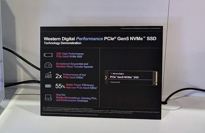
Western Digital's FMS 2024 demonstrations included a preview of their upcoming PCIe 5.0 x4 M.2 2280 NVMe SSDs for mobile workstations and consumer desktops. The Gen 5 client SSD market has been dominated by solutions based on Phison's E26 controller. The first generation products launched with slower NAND flash, while the more recent ones have exceeded the 14 GBps barrier by utilizing Micron's 2400 MT/s 232L 3D TLC. Western Digital has been conservative over the last year or so by focusing more on the mainstream / mid-range market in terms of new product introductions (such as the WD Blue SN5000, WD_BLACK SN770M, and the WD Blue SN580). Their SSD lineup is due for an update with Gen 5 drives being sorely missed. The SSDs being demonstrated at FMS 2024 will end up doing just that.
Western Digital's technology demonstrations in this segment involved two different M.2 2280 SSDs - one for the performance segment, and another for the mainstream market. They both utilize in-house controllers - while the performance segment drive uses a 8-channel controller with DRAM for the flash translation layer, the mainstream one utilizes a 4-channel DRAM-less controller. Both drives being benchmarked live were equipped with BiCS8 218-layer 3D TLC.
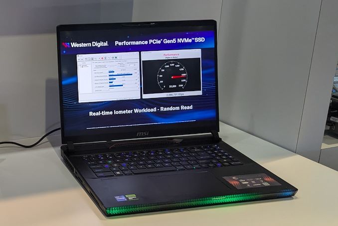
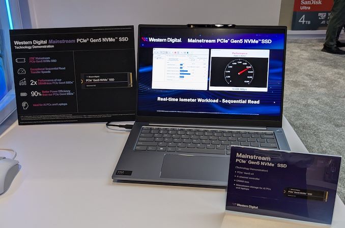
Western Digital is touting the power efficiency of their platform as a key differentiator, promising south of 7W (performance drive) and 5W (mainstream DRAM-less drive) for the complete SSD under stressful traffic. This makes it suitable for use in mobile workstations, but a good fit for desktops as well.
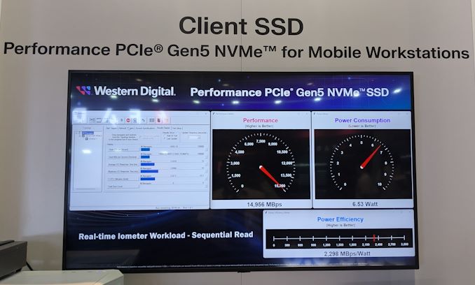
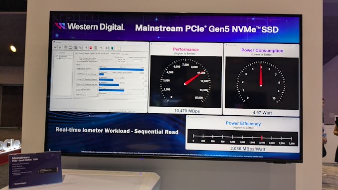
Demonstrated performance numbers indicate almost 15 GBps sequential reads and 2M+ random read IOPS for the performance drive, and 10.7 GBps sequential reads for the mainstream version. Western Digital might have missed the Gen 5 bus as it started out slowly. However, the technology demonstrations with the in-house controller and NAND indicate that WD has caught up just as the Gen 5 market is about to take off.|
Storage
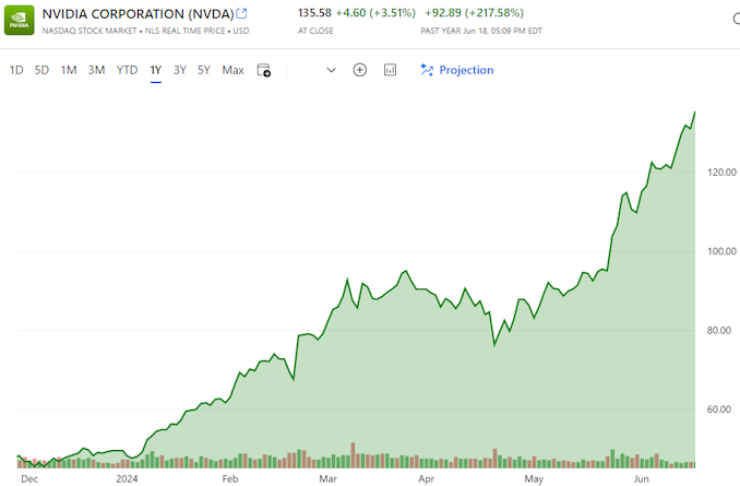
Thanks to the success of the burgeoning market for AI accelerators, NVIDIA has been on a tear this year. And the only place that’s even more apparent than the company’s rapidly growing revenues is in the company’s stock price and market capitalization. After breaking into the top 5 most valuable companies only earlier this year, NVIDIA has reached the apex of Wall Street, closing out today as the world’s most valuable company.
With a closing price of $135.58 on a day that saw NVIDIA’s stock pop up another 3.5%, NVIDIA has topped both Microsoft and Apple in valuation, reaching a market capitalization of $3.335 trillion. This follows a rapid rise in the company’s stock price, which has increased by 47% in the last month alone – particularly on the back of NVIDIA’s most recent estimates-beating earnings report – as well as a recent 10-for-1 stock split. And looking at the company’s performance over a longer time period, NVIDIA’s stock jumped a staggering 218% over the last year, or a mere 3,474% over the last 5 years.
NVIDIA’s ascension continues a trend over the last several years of tech companies all holding the top spots in the market capitalization rankings. Though this is the first time in quite a while that the traditional tech leaders of Apple and Microsoft have been pushed aside.
| Market Capitalization Rankings | ||
| Market Cap | Stock Price | |
| NVIDIA | $3.335T | $135.58 |
| Microsoft | $3.317T | $446.34 |
| Apple | $3.285T | $214.29 |
| Alphabet | $2.170T | $176.45 |
| Amazon | $1.902T | $182.81 |
Driving the rapid growth of NVIDIA and its market capitalization has been demand for AI accelerators from NVIDIA, particularly the company’s server-grade H100, H200, and GH200 accelerators for AI training. As the demand for these products has spiked, NVIDIA has been scaling up accordingly, repeatedly beating market expectations for how many of the accelerators they can ship – and what price they can charge. And despite all that growth, orders for NVIDIA’s high-end accelerators are still backlogged, underscoring how NVIDIA still isn’t meeting the full demands of hyperscalers and other enterprises.
Consequently, NVIDIA’s stock price and market capitalization have been on a tear on the basis of these future expectations. With a price-to-earnings (P/E) ratio of 76.7 – more than twice that of Microsoft or Apple – NVIDIA is priced more like a start-up than a 30-year-old tech company. But then it goes without saying that most 30-year-old tech companies aren’t tripling their revenue in a single year, placing NVIDIA in a rather unique situation at this time.
Like the stock market itself, market capitalizations are highly volatile. And historically speaking, it’s far from guaranteed that NVIDIA will be able to hold the top spot for long, never mind day-to-day fluctuations. NVIDIA, Apple, and Microsoft’s valuations are all within $50 billion (1.%) of each other, so for the moment at least, it’s still a tight race between all three companies. But no matter what happens from here, NVIDIA gets the exceptionally rare claim of having been the most valuable company in the world at some point.
(Carousel image courtesy MSN Money)
GPUs
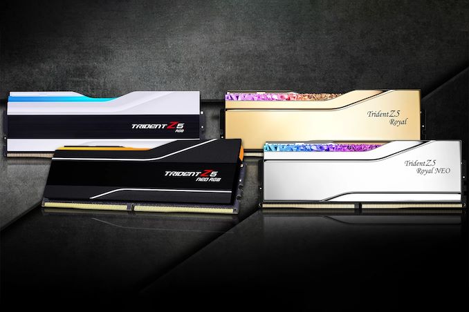
G.Skill on Tuesday introduced its ultra-low-latency DDR5-6400 memory modules that feature a CAS latency of 30 clocks, which appears to be the industry's most aggressive timings yet for DDR5-6400 sticks. The modules will be available for both AMD and Intel CPU-based systems.
With every new generation of DDR memory comes an increase in data transfer rates and an extension of relative latencies. While for the vast majority of applications, the increased bandwidth offsets the performance impact of higher timings, there are applications that favor low latencies. However, shrinking latencies is sometimes harder than increasing data transfer rates, which is why low-latency modules are rare.
Nonetheless, G.Skill has apparently managed to cherry-pick enough DDR5 memory chips and build appropriate printed circuit boards to produce DDR5-6400 modules with CL30 timings, which are substantially lower than the CL46 timings recommended by JEDEC for this speed bin. This means that while JEDEC-standard modules have an absolute latency of 14.375 ns, G.Skill's modules can boast a latency of just 9.375 ns – an approximately 35% decrease.
G.Skill's DDR5-6400 CL30 39-39-102 modules have a capacity of 16 GB and will be available in 32 GB dual-channel kits, though the company does not disclose voltages, which are likely considerably higher than those standardized by JEDEC.
The company plans to make its DDR5-6400 modules available both for AMD systems with EXPO profiles (Trident Z5 Neo RGB and Trident Z5 Royal Neo) and for Intel-powered PCs with XMP 3.0 profiles (Trident Z5 RGB and Trident Z5 Royal). For AMD AM5 systems that have a practical limitation of 6000 MT/s – 6400 MT/s for DDR5 memory (as this is roughly as fast as AMD's Infinity Fabric can operate at with a 1:1 ratio), the new modules will be particularly beneficial for AMD's Ryzen 7000 and Ryzen 9000-series processors.
G.Skill notes that since its modules are non-standard, they will not work with all systems but will operate on high-end motherboards with properly cooled CPUs.
The new ultra-low-latency memory kits will be available worldwide from G.Skill's partners starting in late August 2024. The company did not disclose the pricing of these modules, but since we are talking about premium products that boast unique specifications, they are likely to be priced accordingly.
Memory
Lorem Ipsum is simply dummy text of the printing and typesetting industry. Lorem Ipsum has been the industry's.
While Realtek is best known in the enthusiast space for for its peripheral controllers such as audio codecs and network controllers, the company also has a small-but-respectable SSD controller business that tends to fly under the radar due to its focus on entry-level and mainstream drives. But Realtek's stature in the SSD space is on the rise, as the company is not only planning new PCIe Gen5 SSD controllers, but also their first high-end, DRAM-equipped SSD controller.
For this year's Computex trade show, Realtek laid out a new SSD controller roadmap that calls for the company to release a trio of new SSD controllers over the next couple of years. First up is a new four-channel entry-level PCIe 4.0 controller, the RTS5776DL, which will be joined a bit later by a PCIe 5.0 variant, the RTS5781DL. But most interesting on Realtek's new roadmap is the final chip being planned: the eight-channel, DRAM-equipped RTS5782, which would be the company's first high-end SSD controller, capable of hitting sequential read rates as high as 14GB/second.
| Realtek NVMe SSD Controller Comparison | |||||||||
| RTS5782 | RTS5781DL | RTS5776DL | RTS5772DL | RTS5766DL | |||||
| Market Segment | High-End | Mainstream | Entry-Level | ||||||
| Error Correction | 4K LDPC | 2K LDPC | |||||||
| DRAM | DDR4, LPDDR4(X) | No | No | No | No | ||||
| Host Interface | PCIe 5.0 x4 | PCIe 5.0 x4 | PCIe 4.0 x4 | PCIe 4.0 x4 | PCIe 3.0 x4 | ||||
| NVMe Version | NVMe 2.0 | NVMe 2.0 | NVMe 2.0 | NVMe 1.4 | NVMe 1.4 | ||||
| NAND Channels, Interface Speed | 8 ch, 3600 MT/s |
4 ch, 3600 MT/s |
4 ch, 3600 MT/s |
8 ch, 1600 MT/s |
4 ch, 1200 MT/s |
||||
| Sequential Read | 14 GB/s | 10 GB/s | 7.4 GB/s | 6 GB/s | 3.2 GB/s | ||||
| Sequential Write | 12 GB/s | 10 GB/s | 7.4 GB/s | 6 GB/s | 2.2 GB/s | ||||
| 4KB Random Read IOPS | 2500k | 1400k | 1200k | - | - | ||||
| 4KB Random Write IOPS | 2500k | 1400k | 1200k | - | - | ||||
Diving a bit deeper into Realtek's roadmap, the RTS5776DL is traditional DRAM-less PCIe Gen4 x4 controller with four NAND chann... SSDs
In addition to revealing its roadmap and plans concerning its current leading-edge process technologies, TSMC also shared progress of its N2 node as part of its Symposiums 2024. The company's first 2nm-class fabrication node, and predominantly featuring gate-all-around transistors, according to TSMC N2 has almost achieved its target performance and yield goals, which places it on track to enter high-volume manufacturing in the second half of 2025.
TSMC states that 'N2 development is well on track and N2P is next.' In particular, gate-all-around nanosheet devices currently achieve over 90% of their expected performance, whereas yields of 256 Mb SRAM (32 MB) devices already exceeds 80%, depending on the batch. All of this for a node that is over a year away from mass production.
Meanwhile, average yield of a 256 Mb SRAM was around 70% as of March, 2024, up from around 35% in April, 2023. Device performance has also been improving with higher frequencies being achieved while keeping power consumption in check.
Chip designer interest towards TSMC's first 2nm-class gate-all-around nanosheet transistor-based technology is significant, too. The number of new tape-outs (NTOs) in the first year of N2 is over two-times higher than it was for N5. Though with that said, given TSMC's close working relationship with a handful of high-volume vendors – most notably Appe – NTOs can be a very misleading figure since the first year of a new node at TSMC is capacity constrained, and consequently the bulk of that capacity goes to TSMC's priority partners.
Meanwhile, there were considerably more N5 tapeouts in its second year (some where N5P, of course) and N2 promises to have 2.6X more NTOs in its second year. So the node indeed looks quite promising. In fact, based on TSMC's slides (which we're unfortunately not able to republish), N2 is more popular than N3 in terms of NTOs both in the first and the second years of existence.
When it comes to the second year of N2, in the second half of 2026 TSMC plans to roll out its N2P technology, which promises additional performance and power benefits. N2P is expected to improve frequency by 15% - 20%, reduce power consumption by 30% - 40%, and increase chip density by over 1.15 times compared to N3E, significant benefits to move to all-new GAA nanosheet transistors.
Finally, for those companies that need the best in performance, power, and density, TSMC is poised to offer their A16 process in 2026. That node will also bring in backside power delivery, which will add costs, but is expected to greatly improve performance efficiency and scaling.
Semiconductors






0 Comments