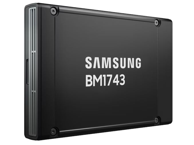

Multiple companies offer high-capacity SSDs, but until recently, only two companies offered high-performance 60 TB-class drives with a PCIe interface: Solidigm and Western Digital. As our colleagues from Blocks & Files discovered, Samsung quietly rolled out its BM1743 61.44 TB solid-state drive in mid-June and now envisions 120 TB-class SSDs based on the same platform.
Samsung's BM1743 61.44 TB features a proprietary controller and relies on Samsung's 7th Generation V-NAND (3D NAND) QLC memory. Moreover, Samsung believes that its 7th Gen V-NAND 'has the potential to accommodate up to 122.88 TB,'
Samsung plans to offer the BM1743 in two form factors: U.2 for PCIe 4.0 x4 to address traditional servers and E3.S for PCIe 5.0 x4 interfaces to address machines designed to offer maximum storage density. BM1743 can address various applications, including AI training and inference, content delivery networks, and read-intensive workloads. To that end, its write endurance is 0.26 drive writes per day (DWPD) over five years.
Regarding performance, Samsung's BM1743 is hardly a champion compared to high-end drives for gaming machines and workstations. The drive can sustainably achieve sequential read speeds of 7,200 MB/s and write speeds of 2,000 MB/s. It can handle up to 1.6 million 4K random reads and 110,000 4K random writes for random operations.
Power consumption details for the BM1743 have not been disclosed, though it is expected to be high. Meanwhile, the drive's key selling point is its massive storage density, which likely outweighs concerns over its absolute power efficiency for intended applications, as a 60 TB SSD still consumes less than multiple storage devices offering similar capacity and performance.
As noted above, Samsung's BM1743 61.44 TB faces limited competition in the market, so its price will be quite high. For example, Solidigm's D5-P5336 61.44 TB SSD costs $6,905. Other companies, such as Kioxia, Micron, and SK Hynix, have not yet introduced their 60TB-class SSDs, which gives Samsung and Solidigm an edge for now.
SSDs

Demand for high-performance processors for AI training is skyrocketing, and consequently so is the demand for the components that go into these processors. So much so that SK hynix this week is very publicly announcing that the company's high-bandwidth memory (HBM) production capacity has already sold out for the rest of 2024, and even most of 2025 has already sold out as well.
SK hynix currently produces various types of HBM memory for customers like Amazon, AMD, Facebook, Google (Broadcom), Intel, Microsoft, and, of course, NVIDIA. The latter is an especially prolific consumer of HBM3 and HBM3E memory for its H100/H200/GH200 accelerators, as NVIDIA is also working to fill what remains an insatiable (and unmet) demand for its accelerators.
As a result, HBM memory orders, which are already placed months in advance, are now backlogging well into 2025 as chip vendors look to secure supplies of the memory stacks critical to their success.
This has made SK hynix the secnd HBM memory vendor in recent months to announce that they've sold out into 2025, following an earlier announcement from Micron regarding its HBM3E production. But of the two announcements, SK hynix's is arguably the most significant yet, as the South Korean firm's HBM production capacity is far greater than Micron's. So while things were merely "interesting" with the smallest of the Big Three memory manufacturers being sold out into 2025, things are taking a more concerning (and constrained) outlook now that SK hynix is as well.
SK hynix currently controls roughly 46% - 49% of HBM market, and its share is not expected to drop significantly in 2025, according to market tracking firm TrendForce. By contrast, Micron's share on HBM memory market is between 4% and 6%. Since HBM supply of both companies is sold out through the most of 2025, we're likely looking at a scenario where over 50% of the industry's total HBM3/HBM3E supply for the coming quarters is already sold out.
This leaves Samsung as the only member of the group not to comment on HBM demand so far. Though with memory being a highly fungible commodity product, it would be surprising if Samsung wasn't facing similar demand. And, ultimately, all of this is pointing towards the indusry entering an HBM3 memory shortage.
Separately, SK hynix said that it is sampling 12-Hi 36GB HBM3E stacks with customers and will begin volume shipments in the third quarter.
Memory
Demand for high-performance processors for AI training is skyrocketing, and consequently so is the demand for the components that go into these processors. So much so that SK hynix this week is very publicly announcing that the company's high-bandwidth memory (HBM) production capacity has already sold out for the rest of 2024, and even most of 2025 has already sold out as well.
SK hynix currently produces various types of HBM memory for customers like Amazon, AMD, Facebook, Google (Broadcom), Intel, Microsoft, and, of course, NVIDIA. The latter is an especially prolific consumer of HBM3 and HBM3E memory for its H100/H200/GH200 accelerators, as NVIDIA is also working to fill what remains an insatiable (and unmet) demand for its accelerators.
As a result, HBM memory orders, which are already placed months in advance, are now backlogging well into 2025 as chip vendors look to secure supplies of the memory stacks critical to their success.
This has made SK hynix the secnd HBM memory vendor in recent months to announce that they've sold out into 2025, following an earlier announcement from Micron regarding its HBM3E production. But of the two announcements, SK hynix's is arguably the most significant yet, as the South Korean firm's HBM production capacity is far greater than Micron's. So while things were merely "interesting" with the smallest of the Big Three memory manufacturers being sold out into 2025, things are taking a more concerning (and constrained) outlook now that SK hynix is as well.
SK hynix currently controls roughly 46% - 49% of HBM market, and its share is not expected to drop significantly in 2025, according to market tracking firm TrendForce. By contrast, Micron's share on HBM memory market is between 4% and 6%. Since HBM supply of both companies is sold out through the most of 2025, we're likely looking at a scenario where over 50% of the industry's total HBM3/HBM3E supply for the coming quarters is already sold out.
This leaves Samsung as the only member of the group not to comment on HBM demand so far. Though with memory being a highly fungible commodity product, it would be surprising if Samsung wasn't facing similar demand. And, ultimately, all of this is pointing towards the indusry entering an HBM3 memory shortage.
Separately, SK hynix said that it is sampling 12-Hi 36GB HBM3E stacks with customers and will begin volume shipments in the third quarter.
Memory![Micron: U.S. Fabs Will Start Operating in 2026 - 2029 <p align="center"><a href="https://www.anandtech.com/show/21459/micron-u-s-fabs-will-start-operating-in-2026-2029"><img src="https://images.anandtech.com/doci/21459/micron-server-datacenter-general-generic-678_575px.jpg" alt="" /></a></p><p><p>When Micron announced plans to build two new fabs in the U.S. in 2022, the company vaguely said both would come online by the decade's end. Then, in 2023, it began to optimize its spending, which pushed production at these fabrication facilities. This week, the company outlined more precise timeframes for when its fabs in <a href="https://www.anandtech.com/show/17573/micron-breaks-ground-on-its-15-billion-euv-dram-fab-in-the-us">Idaho</a> and <a href="https://www.anandtech.com/show/17606/micron-announces-100-billion-us-fab-complex-a-20year-plan">New York</a> will start operations: this will happen from calendar 2026 to calendar 2029.</p>
<p>"<em>These fab construction investments are necessary to support supply growth for the latter half of this decade,</em>" a statement by Micron in its Q3 FY2024 financial results report <a href="https://investors.micron.com/static-files/a531c7f0-fca2-48f3-8f24-79c945aaa2d2">reads</a>. "<em>This Idaho fab will not contribute to meaningful bit supply until fiscal 2027 and the New York construction capex is not expected to contribute to bit supply growth until fiscal 2028 or later. The timing of future [wafer fab equipment] spend in these fabs will be managed to align supply growth with expected demand growth.</em>"</p>
<p>Micron's fiscal year 2027 starts in September 2026, so the new fab near Boise, Idaho, is set to start operations between September 2026 and September 2027. The company's fiscal 2028 starts in September 2027, so the fab will likely begin operations in calendar 2028 or later, probably depending on the demand for DRAM memory in the coming years. That said, Micron's U.S. memory fabs will begin operations between late 2026 and 2029, which aligns with the company's original plans. </p>
<p>Construction of the fab in Idaho is well underway. In contrast, construction of the New York facility has yet to begin as the company is working on regulatory and permitting processes in the state. </p>
<p>Micron's capital expenditure (CaPex) plan for FY2024 is approximately $8.0 billion, with a decrease in year-over-year spending on wafer fabrication equipment (WFE). In Q4 FY2024, the company will spend around $3 billion on fab construction, new wafer fab tools, and various expansions/upgrades.</p>
<p>Looking ahead to FY2025, the company plans a substantial increase in capex, targeting a mid-30s percentage of revenue to support various technological and facility advancements. In particular, it expects its quarterly CapEx to average above the $3 billion level seen in the fourth quarter of FY2024, which means that it plans to spend about $12 billion in its fiscal 2025, which begins in late September.</p>
<p>Half or more of the total CapEx increase in FY2025 (i.e., over $2 billion) will be allocated to constructing new fabs in Idaho and New York. Meanwhile, the FY2025 CapEx will significantly rise to fund high-bandwidth memory (HBM) assembly and testing and the construction of fabrication and back-end facilities. This increase also includes investments in technology transitions to meet growing demand. </p>
<p>"<em>Fab construction in Idaho is underway, and we are working diligently to complete the regulatory and permitting processes in New York,</em>" said Sanjay Mehrotra, chief executive officer of Micron, at the company's conference call with investors and financial analysts (via <a href="https://seekingalpha.com/article/4701253-micron-technology-inc-mu-q3-2024-earnings-call-transcript?source=content_type%3Areact%7Csection%3ATranscripts%7Csection_asset%3ATranscripts%7Cfirst_level_url%3Asymbol%7Cbutton%3ATitle%7Clock_status%3ANo%7Cline%3A1">SeekingAlpha</a>). "<em>This additional leading-edge greenfield capacity, along with continued technology transition investments in our Asia facilities, is required to meet long-term demand in the second half of this decade and beyond. These investments support our objective to maintain our current bit share over time and to grow our memory bit supply in line with long-term industry bit demand.</em>"</p>
</p> Memory](https://lh3.googleusercontent.com/blogger_img_proxy/AEn0k_tIPGqNuftPgOE2nmmXRYBYID78eSSGsdSsd0bi6OXt90q7DE4Klz2sCApnsm8t7hqcb1_baO4RCXiPCqeshCQB-4DrPzv4vEA_9kZLwjOSCU4xCFNz_BwdNOjfs9W9kcVR9RSMZg_jRzOt_A7e7jHGXvxR6Jcy-QtxA6M_A_HXRPg=w72-h72-p-k-no-nu)

When Micron announced plans to build two new fabs in the U.S. in 2022, the company vaguely said both would come online by the decade's end. Then, in 2023, it began to optimize its spending, which pushed production at these fabrication facilities. This week, the company outlined more precise timeframes for when its fabs in Idaho and New York will start operations: this will happen from calendar 2026 to calendar 2029.
"These fab construction investments are necessary to support supply growth for the latter half of this decade," a statement by Micron in its Q3 FY2024 financial results report reads. "This Idaho fab will not contribute to meaningful bit supply until fiscal 2027 and the New York construction capex is not expected to contribute to bit supply growth until fiscal 2028 or later. The timing of future [wafer fab equipment] spend in these fabs will be managed to align supply growth with expected demand growth."
Micron's fiscal year 2027 starts in September 2026, so the new fab near Boise, Idaho, is set to start operations between September 2026 and September 2027. The company's fiscal 2028 starts in September 2027, so the fab will likely begin operations in calendar 2028 or later, probably depending on the demand for DRAM memory in the coming years. That said, Micron's U.S. memory fabs will begin operations between late 2026 and 2029, which aligns with the company's original plans.
Construction of the fab in Idaho is well underway. In contrast, construction of the New York facility has yet to begin as the company is working on regulatory and permitting processes in the state.
Micron's capital expenditure (CaPex) plan for FY2024 is approximately $8.0 billion, with a decrease in year-over-year spending on wafer fabrication equipment (WFE). In Q4 FY2024, the company will spend around $3 billion on fab construction, new wafer fab tools, and various expansions/upgrades.
Looking ahead to FY2025, the company plans a substantial increase in capex, targeting a mid-30s percentage of revenue to support various technological and facility advancements. In particular, it expects its quarterly CapEx to average above the $3 billion level seen in the fourth quarter of FY2024, which means that it plans to spend about $12 billion in its fiscal 2025, which begins in late September.
Half or more of the total CapEx increase in FY2025 (i.e., over $2 billion) will be allocated to constructing new fabs in Idaho and New York. Meanwhile, the FY2025 CapEx will significantly rise to fund high-bandwidth memory (HBM) assembly and testing and the construction of fabrication and back-end facilities. This increase also includes investments in technology transitions to meet growing demand.
"Fab construction in Idaho is underway, and we are working diligently to complete the regulatory and permitting processes in New York," said Sanjay Mehrotra, chief executive officer of Micron, at the company's conference call with investors and financial analysts (via SeekingAlpha). "This additional leading-edge greenfield capacity, along with continued technology transition investments in our Asia facilities, is required to meet long-term demand in the second half of this decade and beyond. These investments support our objective to maintain our current bit share over time and to grow our memory bit supply in line with long-term industry bit demand."
Memory
Lorem Ipsum is simply dummy text of the printing and typesetting industry. Lorem Ipsum has been the industry's.
Demand for high-performance processors for AI training is skyrocketing, and consequently so is the demand for the components that go into these processors. So much so that SK hynix this week is very publicly announcing that the company's high-bandwidth memory (HBM) production capacity has already sold out for the rest of 2024, and even most of 2025 has already sold out as well.
SK hynix currently produces various types of HBM memory for customers like Amazon, AMD, Facebook, Google (Broadcom), Intel, Microsoft, and, of course, NVIDIA. The latter is an especially prolific consumer of HBM3 and HBM3E memory for its H100/H200/GH200 accelerators, as NVIDIA is also working to fill what remains an insatiable (and unmet) demand for its accelerators.
As a result, HBM memory orders, which are already placed months in advance, are now backlogging well into 2025 as chip vendors look to secure supplies of the memory stacks critical to their success.
This has made SK hynix the secnd HBM memory vendor in recent months to announce that they've sold out into 2025, following an earlier announcement from Micron regarding its HBM3E production. But of the two announcements, SK hynix's is arguably the most significant yet, as the South Korean firm's HBM production capacity is far greater than Micron's. So while things were merely "interesting" with the smallest of the Big Three memory manufacturers being sold out into 2025, things are taking a more concerning (and constrained) outlook now that SK hynix is as well.
SK hynix currently controls roughly 46% - 49% of HBM market, and its share is not expected to drop significantly in 2025, according to market tracking firm TrendForce. By contrast, Micron's share on HBM memory market is between 4% and 6%. Since HBM supply of both companies is sold out through the most of 2025, we're likely looking at a scenario where over 50% of the industry's total HBM3/HBM3E supply for the coming quarters is already sold out.
This leaves Samsung as the only member of the group not to comment on HBM demand so far. Though with memory being a highly fungible commodity product, it would be surprising if Samsung wasn't facing similar demand. And, ultimately, all of this is pointing towards the indusry entering an HBM3 memory shortage.
Separately, SK hynix said that it is sampling 12-Hi 36GB HBM3E stacks with customers and will begin volume shipments in the third quarter.
Memory


 QLC memory. Moreover, Samsung believes that its 7<sup>th</sup> Gen V-NAND 'has the potential to accommodate up to 122.88 TB,' </p>
<p>Samsung plans to offer the BM1743 in two form factors: U.2 for PCIe 4.0 x4 to address traditional servers and E3.S for PCIe 5.0 x4 interfaces to address machines designed to offer maximum storage density. BM1743 can address various applications, including AI training and inference, content delivery networks, and read-intensive workloads. To that end, its write endurance is 0.26 drive writes per day (DWPD) over five years.</p>
<p>Regarding performance, Samsung's BM1743 is hardly a champion compared to high-end drives for gaming machines and workstations. The drive can sustainably achieve sequential read speeds of 7,200 MB/s and write speeds of 2,000 MB/s. It can handle up to 1.6 million 4K random reads and 110,000 4K random writes for random operations.</p>
<p>Power consumption details for the BM1743 have not been disclosed, though it is expected to be high. Meanwhile, the drive's key selling point is its massive storage density, which likely outweighs concerns over its absolute power efficiency for intended applications, as a 60 TB SSD still consumes less than multiple storage devices offering similar capacity and performance.</p>
<p>As noted above, Samsung's BM1743 61.44 TB faces limited competition in the market, so its price will be quite high. For example, Solidigm's D5-P5336 61.44 TB SSD costs <a href="https://www.shopblt.com/item/solidigm-d5-p5336-61.44tb-2.5in-pcie/750y_sbfpf2bv614t001.html">$6,905</a>. Other companies, such as Kioxia, Micron, and SK Hynix, have not yet introduced their 60TB-class SSDs, which gives Samsung and Solidigm an edge for now.</p>
</p> SSDs)
 QLC memory. Moreover, Samsung believes that its 7<sup>th</sup> Gen V-NAND 'has the potential to accommodate up to 122.88 TB,' </p>
<p>Samsung plans to offer the BM1743 in two form factors: U.2 for PCIe 4.0 x4 to address traditional servers and E3.S for PCIe 5.0 x4 interfaces to address machines designed to offer maximum storage density. BM1743 can address various applications, including AI training and inference, content delivery networks, and read-intensive workloads. To that end, its write endurance is 0.26 drive writes per day (DWPD) over five years.</p>
<p>Regarding performance, Samsung's BM1743 is hardly a champion compared to high-end drives for gaming machines and workstations. The drive can sustainably achieve sequential read speeds of 7,200 MB/s and write speeds of 2,000 MB/s. It can handle up to 1.6 million 4K random reads and 110,000 4K random writes for random operations.</p>
<p>Power consumption details for the BM1743 have not been disclosed, though it is expected to be high. Meanwhile, the drive's key selling point is its massive storage density, which likely outweighs concerns over its absolute power efficiency for intended applications, as a 60 TB SSD still consumes less than multiple storage devices offering similar capacity and performance.</p>
<p>As noted above, Samsung's BM1743 61.44 TB faces limited competition in the market, so its price will be quite high. For example, Solidigm's D5-P5336 61.44 TB SSD costs <a href="https://www.shopblt.com/item/solidigm-d5-p5336-61.44tb-2.5in-pcie/750y_sbfpf2bv614t001.html">$6,905</a>. Other companies, such as Kioxia, Micron, and SK Hynix, have not yet introduced their 60TB-class SSDs, which gives Samsung and Solidigm an edge for now.</p>
</p> SSDs | https://compbuddey.blogspot.com/2024/07/samsung-joins-60-tb-ssd-club-looking_14.html)
 QLC memory. Moreover, Samsung believes that its 7<sup>th</sup> Gen V-NAND 'has the potential to accommodate up to 122.88 TB,' </p>
<p>Samsung plans to offer the BM1743 in two form factors: U.2 for PCIe 4.0 x4 to address traditional servers and E3.S for PCIe 5.0 x4 interfaces to address machines designed to offer maximum storage density. BM1743 can address various applications, including AI training and inference, content delivery networks, and read-intensive workloads. To that end, its write endurance is 0.26 drive writes per day (DWPD) over five years.</p>
<p>Regarding performance, Samsung's BM1743 is hardly a champion compared to high-end drives for gaming machines and workstations. The drive can sustainably achieve sequential read speeds of 7,200 MB/s and write speeds of 2,000 MB/s. It can handle up to 1.6 million 4K random reads and 110,000 4K random writes for random operations.</p>
<p>Power consumption details for the BM1743 have not been disclosed, though it is expected to be high. Meanwhile, the drive's key selling point is its massive storage density, which likely outweighs concerns over its absolute power efficiency for intended applications, as a 60 TB SSD still consumes less than multiple storage devices offering similar capacity and performance.</p>
<p>As noted above, Samsung's BM1743 61.44 TB faces limited competition in the market, so its price will be quite high. For example, Solidigm's D5-P5336 61.44 TB SSD costs <a href="https://www.shopblt.com/item/solidigm-d5-p5336-61.44tb-2.5in-pcie/750y_sbfpf2bv614t001.html">$6,905</a>. Other companies, such as Kioxia, Micron, and SK Hynix, have not yet introduced their 60TB-class SSDs, which gives Samsung and Solidigm an edge for now.</p>
</p> SSDs&body=https://compbuddey.blogspot.com/2024/07/samsung-joins-60-tb-ssd-club-looking_14.html)
0 Comments