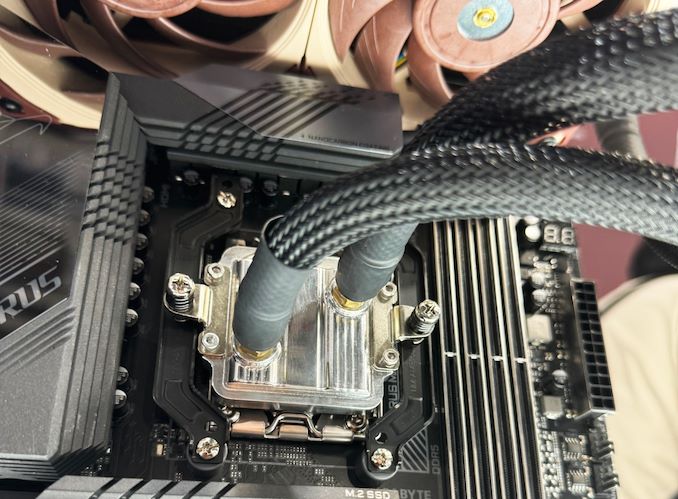

Many companies showed off a range of concept designs during Computex 2024, but perhaps Noctua had one of the coolest. Noctua, primarily known for its air coolers, had a pumpless prototype that showcased Thermisiphon cooling. It looks like a conventional AIO cooler on the surface but is much more efficient, cooler, and quieter than traditional water coolers.
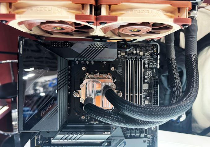
Touching quickly on Thermosiphon cooling, it uses the natural laws of thermodynamics to use heat (the CPU) as a source to turn the liquid to the top, evaporating through the system. This evaporated liquid rises and is pushed into the condenser (radiator), which, in the case of Noctua's cooler, is cooled by fans and turned back into liquid, which then flows back toward the CPU. Not only does Theromsiphon technology use gravity to help aid the flow of liquid, but it is also a highly efficient way of distributing heat as vaporization can absorb heat better, and it doesn't feature any moving parts in the mechanism, aside from the fans, of course.
As with traditional AIO CPU coolers, Noctua's Thermosiphon design has a 240mm radiator with a pair of 120cm Noctua fans, which cools the vapor down and sends it back to the evaporator. While this isn't a new concept and vapor chamber cooling has been used for many years in CPUs and even laptop coolers, Thermosiphon is certainly a technology Noctua thinks it can leverage to ensure better cooling performance and robust reliability.
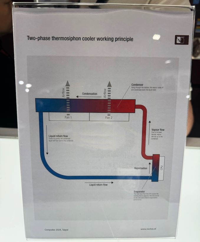
Speaking to Noctua at Computex 2024, they informed me of the benefits and pitfalls of the Thermosiphon technology. In terms of the pros, Thermosiphon cooling in itself has no moving parts, which not only improves reliability but also means there is less to go wrong. Another positive is that even the quietest AIO CPU coolers can be quite noisy, as the water pump that circulates the fluid can cause vibrations, which in turn makes noise. The biggest drawback of implementing Thermosiphon cooling for PCs is that conventional tubing can wear out over time. While adding metal tubing would last longer, it's not flexible, although Noctua said they have discussed this with system integrators.
Although Noctua's Thermosiphon is currently just a proof of concept and sis in the early development stage, there's no launch date or indication it will hit the market. It's an interesting design, and we hope it does eventually come to market.
Cases/Cooling/PSUs

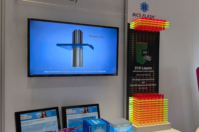
Kioxia's booth at FMS 2024 was a busy one with multiple technology demonstrations keeping visitors occupied. A walk-through of the BiCS 8 manufacturing process was the first to grab my attention. Kioxia and Western Digital announced the sampling of BiCS 8 in March 2023. We had touched briefly upon its CMOS Bonded Array (CBA) scheme in our coverage of Kioxial's 2Tb QLC NAND device and coverage of Western Digital's 128 TB QLC enterprise SSD proof-of-concept demonstration. At Kioxia's booth, we got more insights.
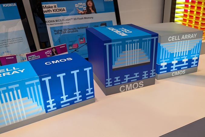
Traditionally, fabrication of flash chips involved placement of the associate logic circuitry (CMOS process) around the periphery of the flash array. The process then moved on to putting the CMOS under the cell array, but the wafer development process was serialized with the CMOS logic getting fabricated first followed by the cell array on top. However, this has some challenges because the cell array requires a high-temperature processing step to ensure higher reliability that can be detrimental to the health of the CMOS logic. Thanks to recent advancements in wafer bonding techniques, the new CBA process allows the CMOS wafer and cell array wafer to be processed independently in parallel and then pieced together, as shown in the models above.
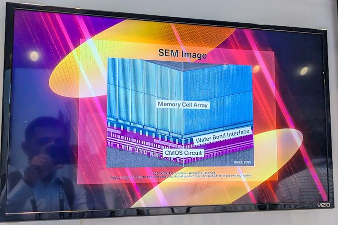
The BiCS 8 3D NAND incorporates 218 layers, compared to 112 layers in BiCS 5 and 162 layers in BiCS 6. The company decided to skip over BiCS 7 (or, rather, it was probably a short-lived generation meant as an internal test vehicle). The generation retains the four-plane charge trap structure of BiCS 6. In its TLC avatar, it is available as a 1 Tbit device. The QLC version is available in two capacities - 1 Tbit and 2 Tbit.
Kioxia also noted that while the number of layers (218) doesn't compare favorably with the latest layer counts from the competition, its lateral scaling / cell shrinkage has enabled it to be competitive in terms of bit density as well as operating speeds (3200 MT/s). For reference, the latest shipping NAND from Micron - the G9 - has 276 layers with a bit density in TLC mode of 21 Gbit/mm2, and operates at up to 3600 MT/s. However, its 232L NAND operates only up to 2400 MT/s and has a bit density of 14.6 Gbit/mm2.
It must be noted that the CBA hybrid bonding process has advantages over the current processes used by other vendors - including Micron's CMOS under array (CuA) and SK hynix's 4D PUC (periphery-under-chip) developed in the late 2010s. It is expected that other NAND vendors will also move eventually to some variant of the hybrid bonding scheme used by Kioxia.
Storage
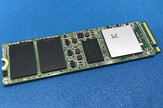
While Realtek is best known in the enthusiast space for for its peripheral controllers such as audio codecs and network controllers, the company also has a small-but-respectable SSD controller business that tends to fly under the radar due to its focus on entry-level and mainstream drives. But Realtek's stature in the SSD space is on the rise, as the company is not only planning new PCIe Gen5 SSD controllers, but also their first high-end, DRAM-equipped SSD controller.
For this year's Computex trade show, Realtek laid out a new SSD controller roadmap that calls for the company to release a trio of new SSD controllers over the next couple of years. First up is a new four-channel entry-level PCIe 4.0 controller, the RTS5776DL, which will be joined a bit later by a PCIe 5.0 variant, the RTS5781DL. But most interesting on Realtek's new roadmap is the final chip being planned: the eight-channel, DRAM-equipped RTS5782, which would be the company's first high-end SSD controller, capable of hitting sequential read rates as high as 14GB/second.
| Realtek NVMe SSD Controller Comparison | |||||||||
| RTS5782 | RTS5781DL | RTS5776DL | RTS5772DL | RTS5766DL | |||||
| Market Segment | High-End | Mainstream | Entry-Level | ||||||
| Error Correction | 4K LDPC | 2K LDPC | |||||||
| DRAM | DDR4, LPDDR4(X) | No | No | No | No | ||||
| Host Interface | PCIe 5.0 x4 | PCIe 5.0 x4 | PCIe 4.0 x4 | PCIe 4.0 x4 | PCIe 3.0 x4 | ||||
| NVMe Version | NVMe 2.0 | NVMe 2.0 | NVMe 2.0 | NVMe 1.4 | NVMe 1.4 | ||||
| NAND Channels, Interface Speed | 8 ch, 3600 MT/s |
4 ch, 3600 MT/s |
4 ch, 3600 MT/s |
8 ch, 1600 MT/s |
4 ch, 1200 MT/s |
||||
| Sequential Read | 14 GB/s | 10 GB/s | 7.4 GB/s | 6 GB/s | 3.2 GB/s | ||||
| Sequential Write | 12 GB/s | 10 GB/s | 7.4 GB/s | 6 GB/s | 2.2 GB/s | ||||
| 4KB Random Read IOPS | 2500k | 1400k | 1200k | - | - | ||||
| 4KB Random Write IOPS | 2500k | 1400k | 1200k | - | - | ||||
Diving a bit deeper into Realtek's roadmap, the RTS5776DL is traditional DRAM-less PCIe Gen4 x4 controller with four NAND chann... SSDs
Kioxia's booth at FMS 2024 was a busy one with multiple technology demonstrations keeping visitors occupied. A walk-through of the BiCS 8 manufacturing process was the first to grab my attention. Kioxia and Western Digital announced the sampling of BiCS 8 in March 2023. We had touched briefly upon its CMOS Bonded Array (CBA) scheme in our coverage of Kioxial's 2Tb QLC NAND device and coverage of Western Digital's 128 TB QLC enterprise SSD proof-of-concept demonstration. At Kioxia's booth, we got more insights.
Traditionally, fabrication of flash chips involved placement of the associate logic circuitry (CMOS process) around the periphery of the flash array. The process then moved on to putting the CMOS under the cell array, but the wafer development process was serialized with the CMOS logic getting fabricated first followed by the cell array on top. However, this has some challenges because the cell array requires a high-temperature processing step to ensure higher reliability that can be detrimental to the health of the CMOS logic. Thanks to recent advancements in wafer bonding techniques, the new CBA process allows the CMOS wafer and cell array wafer to be processed independently in parallel and then pieced together, as shown in the models above.
The BiCS 8 3D NAND incorporates 218 layers, compared to 112 layers in BiCS 5 and 162 layers in BiCS 6. The company decided to skip over BiCS 7 (or, rather, it was probably a short-lived generation meant as an internal test vehicle). The generation retains the four-plane charge trap structure of BiCS 6. In its TLC avatar, it is available as a 1 Tbit device. The QLC version is available in two capacities - 1 Tbit and 2 Tbit.
Kioxia also noted that while the number of layers (218) doesn't compare favorably with the latest layer counts from the competition, its lateral scaling / cell shrinkage has enabled it to be competitive in terms of bit density as well as operating speeds (3200 MT/s). For reference, the latest shipping NAND from Micron - the G9 - has 276 layers with a bit density in TLC mode of 21 Gbit/mm2, and operates at up to 3600 MT/s. However, its 232L NAND operates only up to 2400 MT/s and has a bit density of 14.6 Gbit/mm2.
It must be noted that the CBA hybrid bonding process has advantages over the current processes used by other vendors - including Micron's CMOS under array (CuA) and SK hynix's 4D PUC (periphery-under-chip) developed in the late 2010s. It is expected that other NAND vendors will also move eventually to some variant of the hybrid bonding scheme used by Kioxia.
Storage
While Realtek is best known in the enthusiast space for for its peripheral controllers such as audio codecs and network controllers, the company also has a small-but-respectable SSD controller business that tends to fly under the radar due to its focus on entry-level and mainstream drives. But Realtek's stature in the SSD space is on the rise, as the company is not only planning new PCIe Gen5 SSD controllers, but also their first high-end, DRAM-equipped SSD controller.
For this year's Computex trade show, Realtek laid out a new SSD controller roadmap that calls for the company to release a trio of new SSD controllers over the next couple of years. First up is a new four-channel entry-level PCIe 4.0 controller, the RTS5776DL, which will be joined a bit later by a PCIe 5.0 variant, the RTS5781DL. But most interesting on Realtek's new roadmap is the final chip being planned: the eight-channel, DRAM-equipped RTS5782, which would be the company's first high-end SSD controller, capable of hitting sequential read rates as high as 14GB/second.
| Realtek NVMe SSD Controller Comparison | |||||||||
| RTS5782 | RTS5781DL | RTS5776DL | RTS5772DL | RTS5766DL | |||||
| Market Segment | High-End | Mainstream | Entry-Level | ||||||
| Error Correction | 4K LDPC | 2K LDPC | |||||||
| DRAM | DDR4, LPDDR4(X) | No | No | No | No | ||||
| Host Interface | PCIe 5.0 x4 | PCIe 5.0 x4 | PCIe 4.0 x4 | PCIe 4.0 x4 | PCIe 3.0 x4 | ||||
| NVMe Version | NVMe 2.0 | NVMe 2.0 | NVMe 2.0 | NVMe 1.4 | NVMe 1.4 | ||||
| NAND Channels, Interface Speed | 8 ch, 3600 MT/s |
4 ch, 3600 MT/s |
4 ch, 3600 MT/s |
8 ch, 1600 MT/s |
4 ch, 1200 MT/s |
||||
| Sequential Read | 14 GB/s | 10 GB/s | 7.4 GB/s | 6 GB/s | 3.2 GB/s | ||||
| Sequential Write | 12 GB/s | 10 GB/s | 7.4 GB/s | 6 GB/s | 2.2 GB/s | ||||
| 4KB Random Read IOPS | 2500k | 1400k | 1200k | - | - | ||||
| 4KB Random Write IOPS | 2500k | 1400k | 1200k | - | - | ||||
Diving a bit deeper into Realtek's roadmap, the RTS5776DL is traditional DRAM-less PCIe Gen4 x4 controller with four NAND chann... SSDs

Lorem Ipsum is simply dummy text of the printing and typesetting industry. Lorem Ipsum has been the industry's.
Kioxia's booth at FMS 2024 was a busy one with multiple technology demonstrations keeping visitors occupied. A walk-through of the BiCS 8 manufacturing process was the first to grab my attention. Kioxia and Western Digital announced the sampling of BiCS 8 in March 2023. We had touched briefly upon its CMOS Bonded Array (CBA) scheme in our coverage of Kioxial's 2Tb QLC NAND device and coverage of Western Digital's 128 TB QLC enterprise SSD proof-of-concept demonstration. At Kioxia's booth, we got more insights.
Traditionally, fabrication of flash chips involved placement of the associate logic circuitry (CMOS process) around the periphery of the flash array. The process then moved on to putting the CMOS under the cell array, but the wafer development process was serialized with the CMOS logic getting fabricated first followed by the cell array on top. However, this has some challenges because the cell array requires a high-temperature processing step to ensure higher reliability that can be detrimental to the health of the CMOS logic. Thanks to recent advancements in wafer bonding techniques, the new CBA process allows the CMOS wafer and cell array wafer to be processed independently in parallel and then pieced together, as shown in the models above.
The BiCS 8 3D NAND incorporates 218 layers, compared to 112 layers in BiCS 5 and 162 layers in BiCS 6. The company decided to skip over BiCS 7 (or, rather, it was probably a short-lived generation meant as an internal test vehicle). The generation retains the four-plane charge trap structure of BiCS 6. In its TLC avatar, it is available as a 1 Tbit device. The QLC version is available in two capacities - 1 Tbit and 2 Tbit.
Kioxia also noted that while the number of layers (218) doesn't compare favorably with the latest layer counts from the competition, its lateral scaling / cell shrinkage has enabled it to be competitive in terms of bit density as well as operating speeds (3200 MT/s). For reference, the latest shipping NAND from Micron - the G9 - has 276 layers with a bit density in TLC mode of 21 Gbit/mm2, and operates at up to 3600 MT/s. However, its 232L NAND operates only up to 2400 MT/s and has a bit density of 14.6 Gbit/mm2.
It must be noted that the CBA hybrid bonding process has advantages over the current processes used by other vendors - including Micron's CMOS under array (CuA) and SK hynix's 4D PUC (periphery-under-chip) developed in the late 2010s. It is expected that other NAND vendors will also move eventually to some variant of the hybrid bonding scheme used by Kioxia.
Storage


 as a source to turn the liquid to the top, evaporating through the system. This evaporated liquid rises and is pushed into the condenser (radiator), which, in the case of Noctua's cooler, is cooled by fans and turned back into liquid, which then flows back toward the CPU. Not only does Theromsiphon technology use gravity to help aid the flow of liquid, but it is also a highly efficient way of distributing heat as vaporization can absorb heat better, and it doesn't feature any moving parts in the mechanism, aside from the fans, of course.</p>
<p>As with traditional AIO CPU coolers, Noctua's Thermosiphon design has a 240mm radiator with a pair of 120cm Noctua fans, which cools the vapor down and sends it back to the evaporator. While this isn't a new concept and vapor chamber cooling has been used for many years in CPUs and even laptop coolers, Thermosiphon is certainly a technology Noctua thinks it can leverage to ensure better cooling performance and robust reliability.</p>
<p align="center"><a href="https://www.anandtech.com/show/21446/noctua-shows-off-thermosiphon-based-cpu-cooler-prototype-at-computex-2024"><img alt="" src="https://images.anandtech.com/doci/21446/IMG_1887_575px.jpg" /></a></p>
<p>Speaking to Noctua at Computex 2024, they informed me of the benefits and pitfalls of the Thermosiphon technology. In terms of the pros, Thermosiphon cooling in itself has no moving parts, which not only improves reliability but also means there is less to go wrong. Another positive is that even the quietest AIO CPU coolers can be quite noisy, as the water pump that circulates the fluid can cause vibrations, which in turn makes noise. The biggest drawback of implementing Thermosiphon cooling for PCs is that conventional tubing can wear out over time. While adding metal tubing would last longer, it's not flexible, although Noctua said they have discussed this with system integrators.</p>
<p>Although Noctua's Thermosiphon is currently just a proof of concept and sis in the early development stage, there's no launch date or indication it will hit the market. It's an interesting design, and we hope it does eventually come to market.</p>
</p> Cases/Cooling/PSUs)
 as a source to turn the liquid to the top, evaporating through the system. This evaporated liquid rises and is pushed into the condenser (radiator), which, in the case of Noctua's cooler, is cooled by fans and turned back into liquid, which then flows back toward the CPU. Not only does Theromsiphon technology use gravity to help aid the flow of liquid, but it is also a highly efficient way of distributing heat as vaporization can absorb heat better, and it doesn't feature any moving parts in the mechanism, aside from the fans, of course.</p>
<p>As with traditional AIO CPU coolers, Noctua's Thermosiphon design has a 240mm radiator with a pair of 120cm Noctua fans, which cools the vapor down and sends it back to the evaporator. While this isn't a new concept and vapor chamber cooling has been used for many years in CPUs and even laptop coolers, Thermosiphon is certainly a technology Noctua thinks it can leverage to ensure better cooling performance and robust reliability.</p>
<p align="center"><a href="https://www.anandtech.com/show/21446/noctua-shows-off-thermosiphon-based-cpu-cooler-prototype-at-computex-2024"><img alt="" src="https://images.anandtech.com/doci/21446/IMG_1887_575px.jpg" /></a></p>
<p>Speaking to Noctua at Computex 2024, they informed me of the benefits and pitfalls of the Thermosiphon technology. In terms of the pros, Thermosiphon cooling in itself has no moving parts, which not only improves reliability but also means there is less to go wrong. Another positive is that even the quietest AIO CPU coolers can be quite noisy, as the water pump that circulates the fluid can cause vibrations, which in turn makes noise. The biggest drawback of implementing Thermosiphon cooling for PCs is that conventional tubing can wear out over time. While adding metal tubing would last longer, it's not flexible, although Noctua said they have discussed this with system integrators.</p>
<p>Although Noctua's Thermosiphon is currently just a proof of concept and sis in the early development stage, there's no launch date or indication it will hit the market. It's an interesting design, and we hope it does eventually come to market.</p>
</p> Cases/Cooling/PSUs)
 as a source to turn the liquid to the top, evaporating through the system. This evaporated liquid rises and is pushed into the condenser (radiator), which, in the case of Noctua's cooler, is cooled by fans and turned back into liquid, which then flows back toward the CPU. Not only does Theromsiphon technology use gravity to help aid the flow of liquid, but it is also a highly efficient way of distributing heat as vaporization can absorb heat better, and it doesn't feature any moving parts in the mechanism, aside from the fans, of course.</p>
<p>As with traditional AIO CPU coolers, Noctua's Thermosiphon design has a 240mm radiator with a pair of 120cm Noctua fans, which cools the vapor down and sends it back to the evaporator. While this isn't a new concept and vapor chamber cooling has been used for many years in CPUs and even laptop coolers, Thermosiphon is certainly a technology Noctua thinks it can leverage to ensure better cooling performance and robust reliability.</p>
<p align="center"><a href="https://www.anandtech.com/show/21446/noctua-shows-off-thermosiphon-based-cpu-cooler-prototype-at-computex-2024"><img alt="" src="https://images.anandtech.com/doci/21446/IMG_1887_575px.jpg" /></a></p>
<p>Speaking to Noctua at Computex 2024, they informed me of the benefits and pitfalls of the Thermosiphon technology. In terms of the pros, Thermosiphon cooling in itself has no moving parts, which not only improves reliability but also means there is less to go wrong. Another positive is that even the quietest AIO CPU coolers can be quite noisy, as the water pump that circulates the fluid can cause vibrations, which in turn makes noise. The biggest drawback of implementing Thermosiphon cooling for PCs is that conventional tubing can wear out over time. While adding metal tubing would last longer, it's not flexible, although Noctua said they have discussed this with system integrators.</p>
<p>Although Noctua's Thermosiphon is currently just a proof of concept and sis in the early development stage, there's no launch date or indication it will hit the market. It's an interesting design, and we hope it does eventually come to market.</p>
</p> Cases/Cooling/PSUs | https://compbuddey.blogspot.com/2024/06/noctua-shows-off-thermosiphon-based-cpu_25.html)
 as a source to turn the liquid to the top, evaporating through the system. This evaporated liquid rises and is pushed into the condenser (radiator), which, in the case of Noctua's cooler, is cooled by fans and turned back into liquid, which then flows back toward the CPU. Not only does Theromsiphon technology use gravity to help aid the flow of liquid, but it is also a highly efficient way of distributing heat as vaporization can absorb heat better, and it doesn't feature any moving parts in the mechanism, aside from the fans, of course.</p>
<p>As with traditional AIO CPU coolers, Noctua's Thermosiphon design has a 240mm radiator with a pair of 120cm Noctua fans, which cools the vapor down and sends it back to the evaporator. While this isn't a new concept and vapor chamber cooling has been used for many years in CPUs and even laptop coolers, Thermosiphon is certainly a technology Noctua thinks it can leverage to ensure better cooling performance and robust reliability.</p>
<p align="center"><a href="https://www.anandtech.com/show/21446/noctua-shows-off-thermosiphon-based-cpu-cooler-prototype-at-computex-2024"><img alt="" src="https://images.anandtech.com/doci/21446/IMG_1887_575px.jpg" /></a></p>
<p>Speaking to Noctua at Computex 2024, they informed me of the benefits and pitfalls of the Thermosiphon technology. In terms of the pros, Thermosiphon cooling in itself has no moving parts, which not only improves reliability but also means there is less to go wrong. Another positive is that even the quietest AIO CPU coolers can be quite noisy, as the water pump that circulates the fluid can cause vibrations, which in turn makes noise. The biggest drawback of implementing Thermosiphon cooling for PCs is that conventional tubing can wear out over time. While adding metal tubing would last longer, it's not flexible, although Noctua said they have discussed this with system integrators.</p>
<p>Although Noctua's Thermosiphon is currently just a proof of concept and sis in the early development stage, there's no launch date or indication it will hit the market. It's an interesting design, and we hope it does eventually come to market.</p>
</p> Cases/Cooling/PSUs&body=https://compbuddey.blogspot.com/2024/06/noctua-shows-off-thermosiphon-based-cpu_25.html)


0 Comments