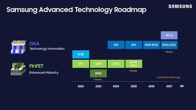

Samsung this week has unveiled its latest process technologies roadmap at the company's Samsung Foundry Forum (SFF) U.S. The new plan covers the evolution of Samsung's 2nm-class production nodes through 2027, including a process technology with a backside power delivery, re-emphasizing plans to bring out a 1.4nm-class node in 2027, and the introduction of a 'high value' 4nm-class manufacturing tech.
Samsung Foundry's key announcements for today are clearly focused on the its 2nm-class process technologies, which are set to enter production in 2025 and will span to 2027, when the company's 1.4-nm class production node is set to enter the scene. Samsung is also adding (or rather, renaming) another 2nm-class node to their roadmap with SF2, which was previously disclosed by Samsung as SF3P and aimed at high-performance devices.
"We have refined and improved the SF3P, resulting in what we now refer to as SF2," a Samsung spokesperson told AnandTech. "This enhanced node incorporates various process design improvements, delivering notable power, performance, and area (PPA) benefits."
| Samsung Foundry for Leading-Edge Nodes Announced on June 12, 2024 Compiled by AnandTech |
||||||||
| HVM Start | 2023 | 2024 | 2025 | 2026 | 2027 | 2027 | ||
| Process | SF3E | SF3 | SF2 (aka SF3P) |
SF2P/SF2X | SF2Z | SF1.4 | ||
| FET | GAAFET | |||||||
| Power Delivery | Frontside | Backside (BSPDN) | ? | |||||
| EUV | 0.33 NA EUV | ? | ? | ? | ? | |||
This is another example of a rebranding of leading-edge fabrication nodes in the recent years by a major chipmaker. Samsung Foundry is not disclosing any specific PPA improvements SF3P has over SF2, and for now is only stating in high-level terms that it will be a better-performing node than the planned SF3P.
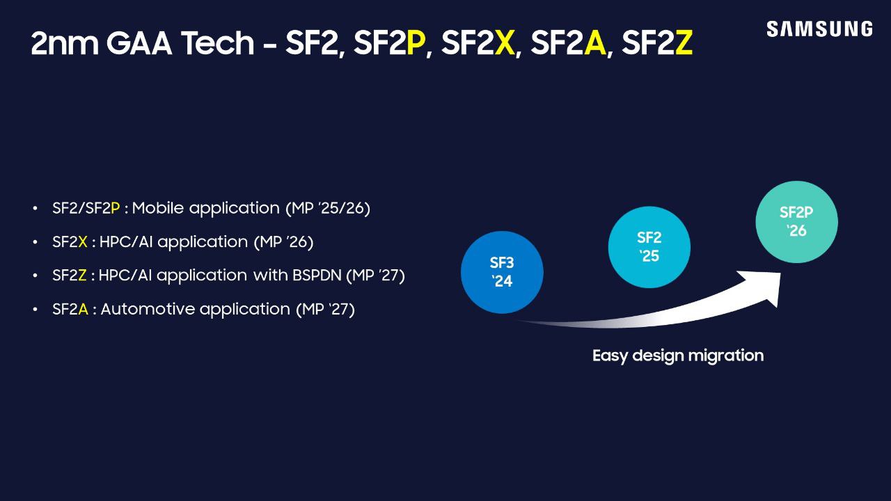
Meanwhile, this week's announcement also includes new information on Samsung's next batch of process nodes, which are planned for 2026 and 2027. In 2026 Samsung will have SF2P, a further refinement of SF2 which incorporates 'faster' yet less dense transistors. That will be followed up in 2027 with SF2Z, which adds backside power delivery to the mix for better and higher quality power delivery. In particular, Samsung is targetting voltate drop (aka IR drop) here, which is an ongoing concern in chip design.
Finally, SF1.4, a 1.4nm-class node, is on track for 2027 as well. Interestingly, however, it looks like it does not feature a backside power delivery. Which, per current roadmaps, would have Samsung as the only foundry not using BSPDN for their first 1.4nm/14Å-class node.
"We have optimized BSPDN and incorporated it for the first time in the SF2Z node we announced today," the spokesperso... Semiconductors


Demand for high-performance processors for AI training is skyrocketing, and consequently so is the demand for the components that go into these processors. So much so that SK hynix this week is very publicly announcing that the company's high-bandwidth memory (HBM) production capacity has already sold out for the rest of 2024, and even most of 2025 has already sold out as well.
SK hynix currently produces various types of HBM memory for customers like Amazon, AMD, Facebook, Google (Broadcom), Intel, Microsoft, and, of course, NVIDIA. The latter is an especially prolific consumer of HBM3 and HBM3E memory for its H100/H200/GH200 accelerators, as NVIDIA is also working to fill what remains an insatiable (and unmet) demand for its accelerators.
As a result, HBM memory orders, which are already placed months in advance, are now backlogging well into 2025 as chip vendors look to secure supplies of the memory stacks critical to their success.
This has made SK hynix the secnd HBM memory vendor in recent months to announce that they've sold out into 2025, following an earlier announcement from Micron regarding its HBM3E production. But of the two announcements, SK hynix's is arguably the most significant yet, as the South Korean firm's HBM production capacity is far greater than Micron's. So while things were merely "interesting" with the smallest of the Big Three memory manufacturers being sold out into 2025, things are taking a more concerning (and constrained) outlook now that SK hynix is as well.
SK hynix currently controls roughly 46% - 49% of HBM market, and its share is not expected to drop significantly in 2025, according to market tracking firm TrendForce. By contrast, Micron's share on HBM memory market is between 4% and 6%. Since HBM supply of both companies is sold out through the most of 2025, we're likely looking at a scenario where over 50% of the industry's total HBM3/HBM3E supply for the coming quarters is already sold out.
This leaves Samsung as the only member of the group not to comment on HBM demand so far. Though with memory being a highly fungible commodity product, it would be surprising if Samsung wasn't facing similar demand. And, ultimately, all of this is pointing towards the indusry entering an HBM3 memory shortage.
Separately, SK hynix said that it is sampling 12-Hi 36GB HBM3E stacks with customers and will begin volume shipments in the third quarter.
Memory
Demand for high-performance processors for AI training is skyrocketing, and consequently so is the demand for the components that go into these processors. So much so that SK hynix this week is very publicly announcing that the company's high-bandwidth memory (HBM) production capacity has already sold out for the rest of 2024, and even most of 2025 has already sold out as well.
SK hynix currently produces various types of HBM memory for customers like Amazon, AMD, Facebook, Google (Broadcom), Intel, Microsoft, and, of course, NVIDIA. The latter is an especially prolific consumer of HBM3 and HBM3E memory for its H100/H200/GH200 accelerators, as NVIDIA is also working to fill what remains an insatiable (and unmet) demand for its accelerators.
As a result, HBM memory orders, which are already placed months in advance, are now backlogging well into 2025 as chip vendors look to secure supplies of the memory stacks critical to their success.
This has made SK hynix the secnd HBM memory vendor in recent months to announce that they've sold out into 2025, following an earlier announcement from Micron regarding its HBM3E production. But of the two announcements, SK hynix's is arguably the most significant yet, as the South Korean firm's HBM production capacity is far greater than Micron's. So while things were merely "interesting" with the smallest of the Big Three memory manufacturers being sold out into 2025, things are taking a more concerning (and constrained) outlook now that SK hynix is as well.
SK hynix currently controls roughly 46% - 49% of HBM market, and its share is not expected to drop significantly in 2025, according to market tracking firm TrendForce. By contrast, Micron's share on HBM memory market is between 4% and 6%. Since HBM supply of both companies is sold out through the most of 2025, we're likely looking at a scenario where over 50% of the industry's total HBM3/HBM3E supply for the coming quarters is already sold out.
This leaves Samsung as the only member of the group not to comment on HBM demand so far. Though with memory being a highly fungible commodity product, it would be surprising if Samsung wasn't facing similar demand. And, ultimately, all of this is pointing towards the indusry entering an HBM3 memory shortage.
Separately, SK hynix said that it is sampling 12-Hi 36GB HBM3E stacks with customers and will begin volume shipments in the third quarter.
Memory![Micron: U.S. Fabs Will Start Operating in 2026 - 2029 <p align="center"><a href="https://www.anandtech.com/show/21459/micron-u-s-fabs-will-start-operating-in-2026-2029"><img src="https://images.anandtech.com/doci/21459/micron-server-datacenter-general-generic-678_575px.jpg" alt="" /></a></p><p><p>When Micron announced plans to build two new fabs in the U.S. in 2022, the company vaguely said both would come online by the decade's end. Then, in 2023, it began to optimize its spending, which pushed production at these fabrication facilities. This week, the company outlined more precise timeframes for when its fabs in <a href="https://www.anandtech.com/show/17573/micron-breaks-ground-on-its-15-billion-euv-dram-fab-in-the-us">Idaho</a> and <a href="https://www.anandtech.com/show/17606/micron-announces-100-billion-us-fab-complex-a-20year-plan">New York</a> will start operations: this will happen from calendar 2026 to calendar 2029.</p>
<p>"<em>These fab construction investments are necessary to support supply growth for the latter half of this decade,</em>" a statement by Micron in its Q3 FY2024 financial results report <a href="https://investors.micron.com/static-files/a531c7f0-fca2-48f3-8f24-79c945aaa2d2">reads</a>. "<em>This Idaho fab will not contribute to meaningful bit supply until fiscal 2027 and the New York construction capex is not expected to contribute to bit supply growth until fiscal 2028 or later. The timing of future [wafer fab equipment] spend in these fabs will be managed to align supply growth with expected demand growth.</em>"</p>
<p>Micron's fiscal year 2027 starts in September 2026, so the new fab near Boise, Idaho, is set to start operations between September 2026 and September 2027. The company's fiscal 2028 starts in September 2027, so the fab will likely begin operations in calendar 2028 or later, probably depending on the demand for DRAM memory in the coming years. That said, Micron's U.S. memory fabs will begin operations between late 2026 and 2029, which aligns with the company's original plans. </p>
<p>Construction of the fab in Idaho is well underway. In contrast, construction of the New York facility has yet to begin as the company is working on regulatory and permitting processes in the state. </p>
<p>Micron's capital expenditure (CaPex) plan for FY2024 is approximately $8.0 billion, with a decrease in year-over-year spending on wafer fabrication equipment (WFE). In Q4 FY2024, the company will spend around $3 billion on fab construction, new wafer fab tools, and various expansions/upgrades.</p>
<p>Looking ahead to FY2025, the company plans a substantial increase in capex, targeting a mid-30s percentage of revenue to support various technological and facility advancements. In particular, it expects its quarterly CapEx to average above the $3 billion level seen in the fourth quarter of FY2024, which means that it plans to spend about $12 billion in its fiscal 2025, which begins in late September.</p>
<p>Half or more of the total CapEx increase in FY2025 (i.e., over $2 billion) will be allocated to constructing new fabs in Idaho and New York. Meanwhile, the FY2025 CapEx will significantly rise to fund high-bandwidth memory (HBM) assembly and testing and the construction of fabrication and back-end facilities. This increase also includes investments in technology transitions to meet growing demand. </p>
<p>"<em>Fab construction in Idaho is underway, and we are working diligently to complete the regulatory and permitting processes in New York,</em>" said Sanjay Mehrotra, chief executive officer of Micron, at the company's conference call with investors and financial analysts (via <a href="https://seekingalpha.com/article/4701253-micron-technology-inc-mu-q3-2024-earnings-call-transcript?source=content_type%3Areact%7Csection%3ATranscripts%7Csection_asset%3ATranscripts%7Cfirst_level_url%3Asymbol%7Cbutton%3ATitle%7Clock_status%3ANo%7Cline%3A1">SeekingAlpha</a>). "<em>This additional leading-edge greenfield capacity, along with continued technology transition investments in our Asia facilities, is required to meet long-term demand in the second half of this decade and beyond. These investments support our objective to maintain our current bit share over time and to grow our memory bit supply in line with long-term industry bit demand.</em>"</p>
</p> Memory](https://lh3.googleusercontent.com/blogger_img_proxy/AEn0k_sMPXJTiFcEdytaL_jl5HTp7GNvXIiFx6im2Yx-LCJE50PEQR9GsKq8Q3vHj8lHhgGctuLHT4iHd5J2AhJ4LO3NrhdM_9rpYmAHH7G-Xz7U2pvqNRCRbfLVEMRjN24GyIio3OoLvNeAO0T91jge23VK51k_XHcFFEtrKAOaldUEitE=w72-h72-p-k-no-nu)

When Micron announced plans to build two new fabs in the U.S. in 2022, the company vaguely said both would come online by the decade's end. Then, in 2023, it began to optimize its spending, which pushed production at these fabrication facilities. This week, the company outlined more precise timeframes for when its fabs in Idaho and New York will start operations: this will happen from calendar 2026 to calendar 2029.
"These fab construction investments are necessary to support supply growth for the latter half of this decade," a statement by Micron in its Q3 FY2024 financial results report reads. "This Idaho fab will not contribute to meaningful bit supply until fiscal 2027 and the New York construction capex is not expected to contribute to bit supply growth until fiscal 2028 or later. The timing of future [wafer fab equipment] spend in these fabs will be managed to align supply growth with expected demand growth."
Micron's fiscal year 2027 starts in September 2026, so the new fab near Boise, Idaho, is set to start operations between September 2026 and September 2027. The company's fiscal 2028 starts in September 2027, so the fab will likely begin operations in calendar 2028 or later, probably depending on the demand for DRAM memory in the coming years. That said, Micron's U.S. memory fabs will begin operations between late 2026 and 2029, which aligns with the company's original plans.
Construction of the fab in Idaho is well underway. In contrast, construction of the New York facility has yet to begin as the company is working on regulatory and permitting processes in the state.
Micron's capital expenditure (CaPex) plan for FY2024 is approximately $8.0 billion, with a decrease in year-over-year spending on wafer fabrication equipment (WFE). In Q4 FY2024, the company will spend around $3 billion on fab construction, new wafer fab tools, and various expansions/upgrades.
Looking ahead to FY2025, the company plans a substantial increase in capex, targeting a mid-30s percentage of revenue to support various technological and facility advancements. In particular, it expects its quarterly CapEx to average above the $3 billion level seen in the fourth quarter of FY2024, which means that it plans to spend about $12 billion in its fiscal 2025, which begins in late September.
Half or more of the total CapEx increase in FY2025 (i.e., over $2 billion) will be allocated to constructing new fabs in Idaho and New York. Meanwhile, the FY2025 CapEx will significantly rise to fund high-bandwidth memory (HBM) assembly and testing and the construction of fabrication and back-end facilities. This increase also includes investments in technology transitions to meet growing demand.
"Fab construction in Idaho is underway, and we are working diligently to complete the regulatory and permitting processes in New York," said Sanjay Mehrotra, chief executive officer of Micron, at the company's conference call with investors and financial analysts (via SeekingAlpha). "This additional leading-edge greenfield capacity, along with continued technology transition investments in our Asia facilities, is required to meet long-term demand in the second half of this decade and beyond. These investments support our objective to maintain our current bit share over time and to grow our memory bit supply in line with long-term industry bit demand."
Memory
Lorem Ipsum is simply dummy text of the printing and typesetting industry. Lorem Ipsum has been the industry's.
Demand for high-performance processors for AI training is skyrocketing, and consequently so is the demand for the components that go into these processors. So much so that SK hynix this week is very publicly announcing that the company's high-bandwidth memory (HBM) production capacity has already sold out for the rest of 2024, and even most of 2025 has already sold out as well.
SK hynix currently produces various types of HBM memory for customers like Amazon, AMD, Facebook, Google (Broadcom), Intel, Microsoft, and, of course, NVIDIA. The latter is an especially prolific consumer of HBM3 and HBM3E memory for its H100/H200/GH200 accelerators, as NVIDIA is also working to fill what remains an insatiable (and unmet) demand for its accelerators.
As a result, HBM memory orders, which are already placed months in advance, are now backlogging well into 2025 as chip vendors look to secure supplies of the memory stacks critical to their success.
This has made SK hynix the secnd HBM memory vendor in recent months to announce that they've sold out into 2025, following an earlier announcement from Micron regarding its HBM3E production. But of the two announcements, SK hynix's is arguably the most significant yet, as the South Korean firm's HBM production capacity is far greater than Micron's. So while things were merely "interesting" with the smallest of the Big Three memory manufacturers being sold out into 2025, things are taking a more concerning (and constrained) outlook now that SK hynix is as well.
SK hynix currently controls roughly 46% - 49% of HBM market, and its share is not expected to drop significantly in 2025, according to market tracking firm TrendForce. By contrast, Micron's share on HBM memory market is between 4% and 6%. Since HBM supply of both companies is sold out through the most of 2025, we're likely looking at a scenario where over 50% of the industry's total HBM3/HBM3E supply for the coming quarters is already sold out.
This leaves Samsung as the only member of the group not to comment on HBM demand so far. Though with memory being a highly fungible commodity product, it would be surprising if Samsung wasn't facing similar demand. And, ultimately, all of this is pointing towards the indusry entering an HBM3 memory shortage.
Separately, SK hynix said that it is sampling 12-Hi 36GB HBM3E stacks with customers and will begin volume shipments in the third quarter.
Memory


 U.S. The new plan covers the evolution of Samsung's 2nm-class production nodes through 2027, including a process technology with a backside power delivery, re-emphasizing plans to bring out a 1.4nm-class node in 2027, and the introduction of a 'high value' 4nm-class manufacturing tech.</p>
<p>Samsung Foundry's key announcements for today are clearly focused on the its 2nm-class process technologies, which are set to enter production in 2025 and will span to 2027, when the company's 1.4-nm class production node is set to enter the scene. Samsung is also adding (or rather, renaming) another 2nm-class node to their roadmap with SF2, which was previously disclosed by Samsung as SF3P and aimed at high-performance devices.</p>
<p>"We have refined and improved the SF3P, resulting in what we now refer to as SF2," a Samsung spokesperson told <em>AnandTech</em>. "This enhanced node incorporates various process design improvements, delivering notable power, performance, and area (PPA) benefits."</p>
<table align="center" border="0" cellpadding="0" cellspacing="1" style="background-color: rgb(246, 246, 246);" width="680">
<tbody>
<tr class="tgrey">
<td align="center" colspan="9">Samsung Foundry for Leading-Edge Nodes<br />
<small>Announced on June 12, 2024<br />
<em>Compiled by AnandTech</em></small></td>
</tr>
<tr class="tlblue">
<td colspan="2" rowspan="1" width="186">HVM Start</td>
<td align="center" valign="middle" width="136">2023</td>
<td align="center" valign="middle" width="136">2024</td>
<td align="center" valign="middle" width="136">2025</td>
<td align="center" valign="middle" width="136">2026</td>
<td align="center" valign="middle" width="136">2027</td>
<td align="center" valign="middle" width="136">2027</td>
</tr>
<tr>
<td class="tlgrey" colspan="2" rowspan="1">Process</td>
<td align="center" valign="middle">SF3E</td>
<td align="center" valign="middle">SF3</td>
<td align="center" rowspan="1" valign="middle">SF2<br />
(aka SF3P)</td>
<td align="center" rowspan="1" valign="middle">SF2P/SF2X</td>
<td align="center" valign="middle">SF2Z</td>
<td align="center" valign="middle">SF1.4</td>
</tr>
<tr>
<td class="tlgrey" colspan="2" rowspan="1">FET</td>
<td align="center" colspan="6" rowspan="1" valign="middle">GAAFET</td>
</tr>
<tr>
<td class="tlgrey" colspan="2" rowspan="1">Power Delivery</td>
<td align="center" colspan="4" rowspan="1" valign="middle">Frontside</td>
<td align="center" valign="middle">Backside (BSPDN)</td>
<td align="center" valign="middle">?</td>
</tr>
<tr>
<td class="tlgrey" colspan="2" rowspan="1">EUV</td>
<td align="center" colspan="2" rowspan="1" valign="middle">0.33 NA EUV</td>
<td align="center" valign="middle">?</td>
<td align="center" valign="middle">?</td>
<td align="center" valign="middle">?</td>
<td align="center" valign="middle">?</td>
</tr>
</tbody>
</table>
<p>This is another example of a rebranding of leading-edge fabrication nodes in the recent years by a major chipmaker. Samsung Foundry is not disclosing any specific PPA improvements SF3P has over SF2, and for now is only stating in high-level terms that it will be a better-performing node than the planned SF3P.</p>
<p align="center"><a href="https://www.anandtech.com/show/21444/samsung-foundry-unveils-updated-roadmap-2nm-evolution-through-2027"><img alt="" src="https://images.anandtech.com/doci/21444/Samsung%202nm%20Process%20Roadmap%20based%20on%20GAA%20Technology.jpeg" style="width: 100%;" /></a></p>
<p>Meanwhile, this week's announcement also includes new information on Samsung's next batch of process nodes, which are planned for 2026 and 2027. In 2026 Samsung will have SF2P, a further refinement of SF2 which incorporates 'faster' yet less dense transistors. That will be followed up in 2027 with SF2Z, which adds backside power delivery to the mix for better and higher quality power delivery. In particular, Samsung is targetting voltate drop (aka IR drop) here, which is an ongoing concern in chip design.</p>
<p>Finally, SF1.4, a 1.4nm-class node, is on track for 2027 as well. Interestingly, however, it looks like it does not feature a backside power delivery. Which, per current roadmaps, would have Samsung as the only foundry not using BSPDN for their first 1.4nm/14<span class="BxUVEf ILfuVd" lang="en"><span class="hgKElc">Å</span></span>-class node.</p>
<p>"We have optimized BSPDN and incorporated it for the first time in the SF2Z node we announced today," the spokesperso... Semiconductors)
 U.S. The new plan covers the evolution of Samsung's 2nm-class production nodes through 2027, including a process technology with a backside power delivery, re-emphasizing plans to bring out a 1.4nm-class node in 2027, and the introduction of a 'high value' 4nm-class manufacturing tech.</p>
<p>Samsung Foundry's key announcements for today are clearly focused on the its 2nm-class process technologies, which are set to enter production in 2025 and will span to 2027, when the company's 1.4-nm class production node is set to enter the scene. Samsung is also adding (or rather, renaming) another 2nm-class node to their roadmap with SF2, which was previously disclosed by Samsung as SF3P and aimed at high-performance devices.</p>
<p>"We have refined and improved the SF3P, resulting in what we now refer to as SF2," a Samsung spokesperson told <em>AnandTech</em>. "This enhanced node incorporates various process design improvements, delivering notable power, performance, and area (PPA) benefits."</p>
<table align="center" border="0" cellpadding="0" cellspacing="1" style="background-color: rgb(246, 246, 246);" width="680">
<tbody>
<tr class="tgrey">
<td align="center" colspan="9">Samsung Foundry for Leading-Edge Nodes<br />
<small>Announced on June 12, 2024<br />
<em>Compiled by AnandTech</em></small></td>
</tr>
<tr class="tlblue">
<td colspan="2" rowspan="1" width="186">HVM Start</td>
<td align="center" valign="middle" width="136">2023</td>
<td align="center" valign="middle" width="136">2024</td>
<td align="center" valign="middle" width="136">2025</td>
<td align="center" valign="middle" width="136">2026</td>
<td align="center" valign="middle" width="136">2027</td>
<td align="center" valign="middle" width="136">2027</td>
</tr>
<tr>
<td class="tlgrey" colspan="2" rowspan="1">Process</td>
<td align="center" valign="middle">SF3E</td>
<td align="center" valign="middle">SF3</td>
<td align="center" rowspan="1" valign="middle">SF2<br />
(aka SF3P)</td>
<td align="center" rowspan="1" valign="middle">SF2P/SF2X</td>
<td align="center" valign="middle">SF2Z</td>
<td align="center" valign="middle">SF1.4</td>
</tr>
<tr>
<td class="tlgrey" colspan="2" rowspan="1">FET</td>
<td align="center" colspan="6" rowspan="1" valign="middle">GAAFET</td>
</tr>
<tr>
<td class="tlgrey" colspan="2" rowspan="1">Power Delivery</td>
<td align="center" colspan="4" rowspan="1" valign="middle">Frontside</td>
<td align="center" valign="middle">Backside (BSPDN)</td>
<td align="center" valign="middle">?</td>
</tr>
<tr>
<td class="tlgrey" colspan="2" rowspan="1">EUV</td>
<td align="center" colspan="2" rowspan="1" valign="middle">0.33 NA EUV</td>
<td align="center" valign="middle">?</td>
<td align="center" valign="middle">?</td>
<td align="center" valign="middle">?</td>
<td align="center" valign="middle">?</td>
</tr>
</tbody>
</table>
<p>This is another example of a rebranding of leading-edge fabrication nodes in the recent years by a major chipmaker. Samsung Foundry is not disclosing any specific PPA improvements SF3P has over SF2, and for now is only stating in high-level terms that it will be a better-performing node than the planned SF3P.</p>
<p align="center"><a href="https://www.anandtech.com/show/21444/samsung-foundry-unveils-updated-roadmap-2nm-evolution-through-2027"><img alt="" src="https://images.anandtech.com/doci/21444/Samsung%202nm%20Process%20Roadmap%20based%20on%20GAA%20Technology.jpeg" style="width: 100%;" /></a></p>
<p>Meanwhile, this week's announcement also includes new information on Samsung's next batch of process nodes, which are planned for 2026 and 2027. In 2026 Samsung will have SF2P, a further refinement of SF2 which incorporates 'faster' yet less dense transistors. That will be followed up in 2027 with SF2Z, which adds backside power delivery to the mix for better and higher quality power delivery. In particular, Samsung is targetting voltate drop (aka IR drop) here, which is an ongoing concern in chip design.</p>
<p>Finally, SF1.4, a 1.4nm-class node, is on track for 2027 as well. Interestingly, however, it looks like it does not feature a backside power delivery. Which, per current roadmaps, would have Samsung as the only foundry not using BSPDN for their first 1.4nm/14<span class="BxUVEf ILfuVd" lang="en"><span class="hgKElc">Å</span></span>-class node.</p>
<p>"We have optimized BSPDN and incorporated it for the first time in the SF2Z node we announced today," the spokesperso... Semiconductors | https://compbuddey.blogspot.com/2024/07/samsung-foundry-unveils-updated-roadmap_14.html)
 U.S. The new plan covers the evolution of Samsung's 2nm-class production nodes through 2027, including a process technology with a backside power delivery, re-emphasizing plans to bring out a 1.4nm-class node in 2027, and the introduction of a 'high value' 4nm-class manufacturing tech.</p>
<p>Samsung Foundry's key announcements for today are clearly focused on the its 2nm-class process technologies, which are set to enter production in 2025 and will span to 2027, when the company's 1.4-nm class production node is set to enter the scene. Samsung is also adding (or rather, renaming) another 2nm-class node to their roadmap with SF2, which was previously disclosed by Samsung as SF3P and aimed at high-performance devices.</p>
<p>"We have refined and improved the SF3P, resulting in what we now refer to as SF2," a Samsung spokesperson told <em>AnandTech</em>. "This enhanced node incorporates various process design improvements, delivering notable power, performance, and area (PPA) benefits."</p>
<table align="center" border="0" cellpadding="0" cellspacing="1" style="background-color: rgb(246, 246, 246);" width="680">
<tbody>
<tr class="tgrey">
<td align="center" colspan="9">Samsung Foundry for Leading-Edge Nodes<br />
<small>Announced on June 12, 2024<br />
<em>Compiled by AnandTech</em></small></td>
</tr>
<tr class="tlblue">
<td colspan="2" rowspan="1" width="186">HVM Start</td>
<td align="center" valign="middle" width="136">2023</td>
<td align="center" valign="middle" width="136">2024</td>
<td align="center" valign="middle" width="136">2025</td>
<td align="center" valign="middle" width="136">2026</td>
<td align="center" valign="middle" width="136">2027</td>
<td align="center" valign="middle" width="136">2027</td>
</tr>
<tr>
<td class="tlgrey" colspan="2" rowspan="1">Process</td>
<td align="center" valign="middle">SF3E</td>
<td align="center" valign="middle">SF3</td>
<td align="center" rowspan="1" valign="middle">SF2<br />
(aka SF3P)</td>
<td align="center" rowspan="1" valign="middle">SF2P/SF2X</td>
<td align="center" valign="middle">SF2Z</td>
<td align="center" valign="middle">SF1.4</td>
</tr>
<tr>
<td class="tlgrey" colspan="2" rowspan="1">FET</td>
<td align="center" colspan="6" rowspan="1" valign="middle">GAAFET</td>
</tr>
<tr>
<td class="tlgrey" colspan="2" rowspan="1">Power Delivery</td>
<td align="center" colspan="4" rowspan="1" valign="middle">Frontside</td>
<td align="center" valign="middle">Backside (BSPDN)</td>
<td align="center" valign="middle">?</td>
</tr>
<tr>
<td class="tlgrey" colspan="2" rowspan="1">EUV</td>
<td align="center" colspan="2" rowspan="1" valign="middle">0.33 NA EUV</td>
<td align="center" valign="middle">?</td>
<td align="center" valign="middle">?</td>
<td align="center" valign="middle">?</td>
<td align="center" valign="middle">?</td>
</tr>
</tbody>
</table>
<p>This is another example of a rebranding of leading-edge fabrication nodes in the recent years by a major chipmaker. Samsung Foundry is not disclosing any specific PPA improvements SF3P has over SF2, and for now is only stating in high-level terms that it will be a better-performing node than the planned SF3P.</p>
<p align="center"><a href="https://www.anandtech.com/show/21444/samsung-foundry-unveils-updated-roadmap-2nm-evolution-through-2027"><img alt="" src="https://images.anandtech.com/doci/21444/Samsung%202nm%20Process%20Roadmap%20based%20on%20GAA%20Technology.jpeg" style="width: 100%;" /></a></p>
<p>Meanwhile, this week's announcement also includes new information on Samsung's next batch of process nodes, which are planned for 2026 and 2027. In 2026 Samsung will have SF2P, a further refinement of SF2 which incorporates 'faster' yet less dense transistors. That will be followed up in 2027 with SF2Z, which adds backside power delivery to the mix for better and higher quality power delivery. In particular, Samsung is targetting voltate drop (aka IR drop) here, which is an ongoing concern in chip design.</p>
<p>Finally, SF1.4, a 1.4nm-class node, is on track for 2027 as well. Interestingly, however, it looks like it does not feature a backside power delivery. Which, per current roadmaps, would have Samsung as the only foundry not using BSPDN for their first 1.4nm/14<span class="BxUVEf ILfuVd" lang="en"><span class="hgKElc">Å</span></span>-class node.</p>
<p>"We have optimized BSPDN and incorporated it for the first time in the SF2Z node we announced today," the spokesperso... Semiconductors&body=https://compbuddey.blogspot.com/2024/07/samsung-foundry-unveils-updated-roadmap_14.html)
0 Comments