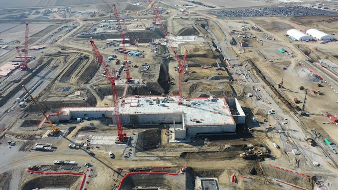

Intel and the United States Department of Commerce announced on Wednesday that they had inked a preliminary agreement under which Intel will receive $8.5 billion in direct funding under the CHIPS and Science Act. Furthermore, Intel is being made eligible for $11 billion in low-interest loans under the same law, and is being given access to a 25% investment tax credit on up to $100 billion of capital expenditures over the next five years. The funds from the long-awaited announcement will be used to expand or build new Intel's semiconductor manufacturing plants in Arizona, New Mexico, Ohio, and Oregon, potentially creating up to 30,000 jobs.
"Today is a defining moment for the U.S. and Intel as we work to power the next great chapter of American semiconductor innovation," said Intel CEO Pat Gelsinger. "AI is supercharging the digital revolution and everything digital needs semiconductors. CHIPS Act support will help to ensure that Intel and the U.S. stay at the forefront of the AI era as we build a resilient and sustainable semiconductor supply chain to power our nation's future."
Intel is working on several important projects, including new semiconductor production facilities and advanced packaging facilities. On the fab front, there are three ongoing projects:
Regarding advanced packaging facilities, Intel is about to complete the conversion of two of its fabs in its Silicon Mesa campus in New Mexico to advanced packaging facilities. These facilities will be crucial to building next-generation multi-chipset processors for clients, data center, and AI applications in the coming years, and which will be the largest advanced packaging operation in the US. Meanwhile, with advanced packaging capacity in New Mexico already in place, the state is set to concentrate vast advanced packaging capabilities to support Intel's ramp of leading-edge fabs in Arizona, Ohio, and Oregon.
To receive both the $8.5 billion in direct funding and the $11 billion in low-interest, long-term loans, Intel must comply with the terms set in the so-called preliminary memorandum of terms (PMTs). The PMT specifies that receiving direct funding and federal loans will only be provided after thoroughly reviewing and negotiating detailed agreements. These financial awards also depend on meeting specific milestone goals, which are not public, but are thought to include terms concerning investments, timing, and workforce developments. Finally, all of this funding is subject to the availability of remaining CHIPS Act funds.
On top of this direct financial assistance, if Intel meets the U.S. government's requirements, it can also access a 25% tax credit on up to $100 billion of qualified capital expenditures over the next five years. This will make Intel's CapEx – the most expensive part of building and outfitting a chip fab – 'cheaper' for the company and stimulate it to invest in the U.S.
"With this agreement, we are helping to incentivize over $100 billion in investments from Intel – marking one of the largest investments ever in U.S. semiconductor manufacturing, which will create over 30,000 good-paying jobs and ignite the next generation of innovation," said U.S. Secretary of Commerce Gina Raimondo. "This announcement is the culmination of years of work by President Biden and bipartisan efforts in Congress to ensure that the leading-edge chips we need to secure our economic and national security are made in the U.S."
Semiconductors

Demand for high-performance processors for AI training is skyrocketing, and consequently so is the demand for the components that go into these processors. So much so that SK hynix this week is very publicly announcing that the company's high-bandwidth memory (HBM) production capacity has already sold out for the rest of 2024, and even most of 2025 has already sold out as well.
SK hynix currently produces various types of HBM memory for customers like Amazon, AMD, Facebook, Google (Broadcom), Intel, Microsoft, and, of course, NVIDIA. The latter is an especially prolific consumer of HBM3 and HBM3E memory for its H100/H200/GH200 accelerators, as NVIDIA is also working to fill what remains an insatiable (and unmet) demand for its accelerators.
As a result, HBM memory orders, which are already placed months in advance, are now backlogging well into 2025 as chip vendors look to secure supplies of the memory stacks critical to their success.
This has made SK hynix the secnd HBM memory vendor in recent months to announce that they've sold out into 2025, following an earlier announcement from Micron regarding its HBM3E production. But of the two announcements, SK hynix's is arguably the most significant yet, as the South Korean firm's HBM production capacity is far greater than Micron's. So while things were merely "interesting" with the smallest of the Big Three memory manufacturers being sold out into 2025, things are taking a more concerning (and constrained) outlook now that SK hynix is as well.
SK hynix currently controls roughly 46% - 49% of HBM market, and its share is not expected to drop significantly in 2025, according to market tracking firm TrendForce. By contrast, Micron's share on HBM memory market is between 4% and 6%. Since HBM supply of both companies is sold out through the most of 2025, we're likely looking at a scenario where over 50% of the industry's total HBM3/HBM3E supply for the coming quarters is already sold out.
This leaves Samsung as the only member of the group not to comment on HBM demand so far. Though with memory being a highly fungible commodity product, it would be surprising if Samsung wasn't facing similar demand. And, ultimately, all of this is pointing towards the indusry entering an HBM3 memory shortage.
Separately, SK hynix said that it is sampling 12-Hi 36GB HBM3E stacks with customers and will begin volume shipments in the third quarter.
Memory
Lorem Ipsum is simply dummy text of the printing and typesetting industry. Lorem Ipsum has been the industry's.
Demand for high-performance processors for AI training is skyrocketing, and consequently so is the demand for the components that go into these processors. So much so that SK hynix this week is very publicly announcing that the company's high-bandwidth memory (HBM) production capacity has already sold out for the rest of 2024, and even most of 2025 has already sold out as well.
SK hynix currently produces various types of HBM memory for customers like Amazon, AMD, Facebook, Google (Broadcom), Intel, Microsoft, and, of course, NVIDIA. The latter is an especially prolific consumer of HBM3 and HBM3E memory for its H100/H200/GH200 accelerators, as NVIDIA is also working to fill what remains an insatiable (and unmet) demand for its accelerators.
As a result, HBM memory orders, which are already placed months in advance, are now backlogging well into 2025 as chip vendors look to secure supplies of the memory stacks critical to their success.
This has made SK hynix the secnd HBM memory vendor in recent months to announce that they've sold out into 2025, following an earlier announcement from Micron regarding its HBM3E production. But of the two announcements, SK hynix's is arguably the most significant yet, as the South Korean firm's HBM production capacity is far greater than Micron's. So while things were merely "interesting" with the smallest of the Big Three memory manufacturers being sold out into 2025, things are taking a more concerning (and constrained) outlook now that SK hynix is as well.
SK hynix currently controls roughly 46% - 49% of HBM market, and its share is not expected to drop significantly in 2025, according to market tracking firm TrendForce. By contrast, Micron's share on HBM memory market is between 4% and 6%. Since HBM supply of both companies is sold out through the most of 2025, we're likely looking at a scenario where over 50% of the industry's total HBM3/HBM3E supply for the coming quarters is already sold out.
This leaves Samsung as the only member of the group not to comment on HBM demand so far. Though with memory being a highly fungible commodity product, it would be surprising if Samsung wasn't facing similar demand. And, ultimately, all of this is pointing towards the indusry entering an HBM3 memory shortage.
Separately, SK hynix said that it is sampling 12-Hi 36GB HBM3E stacks with customers and will begin volume shipments in the third quarter.
Memory


. The PMT specifies that receiving direct funding and federal loans will only be provided after thoroughly reviewing and negotiating detailed agreements. These financial awards also depend on meeting specific milestone goals, which are not public, but are thought to include terms concerning investments, timing, and workforce developments. Finally, all of this funding is subject to the availability of remaining CHIPS Act funds.</p>
<p>On top of this direct financial assistance, if Intel meets the U.S. government's requirements, it can also access a 25% tax credit on up to $100 billion of qualified capital expenditures over the next five years. This will make Intel's CapEx – the most expensive part of building and outfitting a chip fab – 'cheaper' for the company and stimulate it to invest in the U.S.</p>
<p>"<em>With this agreement, we are helping to incentivize over $100 billion in investments from Intel – marking one of the largest investments ever in U.S. semiconductor manufacturing, which will create over 30,000 good-paying jobs and ignite the next generation of innovation,</em>" said U.S. Secretary of Commerce Gina Raimondo. "<em>This announcement is the culmination of years of work by President Biden and bipartisan efforts in Congress to ensure that the leading-edge chips we need to secure our economic and national security are made in the U.S.</em>"</p>
</p> Semiconductors)
. The PMT specifies that receiving direct funding and federal loans will only be provided after thoroughly reviewing and negotiating detailed agreements. These financial awards also depend on meeting specific milestone goals, which are not public, but are thought to include terms concerning investments, timing, and workforce developments. Finally, all of this funding is subject to the availability of remaining CHIPS Act funds.</p>
<p>On top of this direct financial assistance, if Intel meets the U.S. government's requirements, it can also access a 25% tax credit on up to $100 billion of qualified capital expenditures over the next five years. This will make Intel's CapEx – the most expensive part of building and outfitting a chip fab – 'cheaper' for the company and stimulate it to invest in the U.S.</p>
<p>"<em>With this agreement, we are helping to incentivize over $100 billion in investments from Intel – marking one of the largest investments ever in U.S. semiconductor manufacturing, which will create over 30,000 good-paying jobs and ignite the next generation of innovation,</em>" said U.S. Secretary of Commerce Gina Raimondo. "<em>This announcement is the culmination of years of work by President Biden and bipartisan efforts in Congress to ensure that the leading-edge chips we need to secure our economic and national security are made in the U.S.</em>"</p>
</p> Semiconductors | https://compbuddey.blogspot.com/2024/04/intel-to-receive-85b-in-chips-act_5.html)
. The PMT specifies that receiving direct funding and federal loans will only be provided after thoroughly reviewing and negotiating detailed agreements. These financial awards also depend on meeting specific milestone goals, which are not public, but are thought to include terms concerning investments, timing, and workforce developments. Finally, all of this funding is subject to the availability of remaining CHIPS Act funds.</p>
<p>On top of this direct financial assistance, if Intel meets the U.S. government's requirements, it can also access a 25% tax credit on up to $100 billion of qualified capital expenditures over the next five years. This will make Intel's CapEx – the most expensive part of building and outfitting a chip fab – 'cheaper' for the company and stimulate it to invest in the U.S.</p>
<p>"<em>With this agreement, we are helping to incentivize over $100 billion in investments from Intel – marking one of the largest investments ever in U.S. semiconductor manufacturing, which will create over 30,000 good-paying jobs and ignite the next generation of innovation,</em>" said U.S. Secretary of Commerce Gina Raimondo. "<em>This announcement is the culmination of years of work by President Biden and bipartisan efforts in Congress to ensure that the leading-edge chips we need to secure our economic and national security are made in the U.S.</em>"</p>
</p> Semiconductors&body=https://compbuddey.blogspot.com/2024/04/intel-to-receive-85b-in-chips-act_5.html)
0 Comments