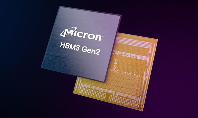

Being the first company to ship HBM3E memory has its perks for Micron, as the company has revealed that is has managed to sell out the entire supply of its advanced high-bandwidth memory for 2024, while most of their 2025 production has been allocated, as well. Micron's HBM3E memory (or how Micron alternatively calls it, HBM3 Gen2) was one of the first to be qualified for NVIDIA's updated H200/GH200 accelerators, so it looks like the DRAM maker will be a key supplier to the green company.
"Our HBM is sold out for calendar 2024, and the overwhelming majority of our 2025 supply has already been allocated," said Sanjay Mehrotra, chief executive of Micron, in prepared remarks for the company's earnings call this week. "We continue to expect HBM bit share equivalent to our overall DRAM bit share sometime in calendar 2025."
Micron's first HBM3E product is an 8-Hi 24 GB stack with a 1024-bit interface, 9.2 GT/s data transfer rate, and a total bandwidth of 1.2 TB/s. NVIDIA's H200 accelerator for artificial intelligence and high-performance computing will use six of these cubes, providing a total of 141 GB of accessible high-bandwidth memory.
"We are on track to generate several hundred million dollars of revenue from HBM in fiscal 2024 and expect HBM revenues to be accretive to our DRAM and overall gross margins starting in the fiscal third quarter," said Mehrotra.
The company has also began sampling its 12-Hi 36 GB stacks that offer a 50% more capacity. These KGSDs will ramp in 2025 and will be used for next generations of AI products. Meanwhile, it does not look like NVIDIA's B100 and B200 are going to use 36 GB HBM3E stacks, at least initially.
Demand for artificial intelligence servers set records last year, and it looks like it is going to remain high this year as well. Some analysts believe that NVIDIA's A100 and H100 processors (as well as their various derivatives) commanded as much as 80% of the entire AI processor market in 2023. And while this year NVIDIA will face tougher competition from AMD, AWS, D-Matrix, Intel, Tenstorrent, and other companies on the inference front, it looks like NVIDIA's H200 will still be the processor of choice for AI training, especially for big players like Meta and Microsoft, who already run fleets consisting of hundreds of thousands of NVIDIA accelerators. With that in mind, being a primary supplier of HBM3E for NVIDIA's H200 is a big deal for Micron as it enables it to finally capture a sizeable chunk of the HBM market, which is currently dominated by SK Hynix and Samsung, and where Micron controlled only about 10% as of last year.
Meanwhile, since every DRAM device inside an HBM stack has a wide interface, it is physically bigger than regular DDR4 or DDR5 ICs. As a result, the ramp of HBM3E memory will affect bit supply of commodity DRAMs from Micron, the company said.
"The ramp of HBM production will constrain supply growth in non-HBM products," Mehrotra said. "Industrywide, HBM3E consumes approximately three times the wafer supply as DDR5 to produce a given number of bits in the same technology node."
Memory

Demand for high-performance processors for AI training is skyrocketing, and consequently so is the demand for the components that go into these processors. So much so that SK hynix this week is very publicly announcing that the company's high-bandwidth memory (HBM) production capacity has already sold out for the rest of 2024, and even most of 2025 has already sold out as well.
SK hynix currently produces various types of HBM memory for customers like Amazon, AMD, Facebook, Google (Broadcom), Intel, Microsoft, and, of course, NVIDIA. The latter is an especially prolific consumer of HBM3 and HBM3E memory for its H100/H200/GH200 accelerators, as NVIDIA is also working to fill what remains an insatiable (and unmet) demand for its accelerators.
As a result, HBM memory orders, which are already placed months in advance, are now backlogging well into 2025 as chip vendors look to secure supplies of the memory stacks critical to their success.
This has made SK hynix the secnd HBM memory vendor in recent months to announce that they've sold out into 2025, following an earlier announcement from Micron regarding its HBM3E production. But of the two announcements, SK hynix's is arguably the most significant yet, as the South Korean firm's HBM production capacity is far greater than Micron's. So while things were merely "interesting" with the smallest of the Big Three memory manufacturers being sold out into 2025, things are taking a more concerning (and constrained) outlook now that SK hynix is as well.
SK hynix currently controls roughly 46% - 49% of HBM market, and its share is not expected to drop significantly in 2025, according to market tracking firm TrendForce. By contrast, Micron's share on HBM memory market is between 4% and 6%. Since HBM supply of both companies is sold out through the most of 2025, we're likely looking at a scenario where over 50% of the industry's total HBM3/HBM3E supply for the coming quarters is already sold out.
This leaves Samsung as the only member of the group not to comment on HBM demand so far. Though with memory being a highly fungible commodity product, it would be surprising if Samsung wasn't facing similar demand. And, ultimately, all of this is pointing towards the indusry entering an HBM3 memory shortage.
Separately, SK hynix said that it is sampling 12-Hi 36GB HBM3E stacks with customers and will begin volume shipments in the third quarter.
Memory
Lorem Ipsum is simply dummy text of the printing and typesetting industry. Lorem Ipsum has been the industry's.
Demand for high-performance processors for AI training is skyrocketing, and consequently so is the demand for the components that go into these processors. So much so that SK hynix this week is very publicly announcing that the company's high-bandwidth memory (HBM) production capacity has already sold out for the rest of 2024, and even most of 2025 has already sold out as well.
SK hynix currently produces various types of HBM memory for customers like Amazon, AMD, Facebook, Google (Broadcom), Intel, Microsoft, and, of course, NVIDIA. The latter is an especially prolific consumer of HBM3 and HBM3E memory for its H100/H200/GH200 accelerators, as NVIDIA is also working to fill what remains an insatiable (and unmet) demand for its accelerators.
As a result, HBM memory orders, which are already placed months in advance, are now backlogging well into 2025 as chip vendors look to secure supplies of the memory stacks critical to their success.
This has made SK hynix the secnd HBM memory vendor in recent months to announce that they've sold out into 2025, following an earlier announcement from Micron regarding its HBM3E production. But of the two announcements, SK hynix's is arguably the most significant yet, as the South Korean firm's HBM production capacity is far greater than Micron's. So while things were merely "interesting" with the smallest of the Big Three memory manufacturers being sold out into 2025, things are taking a more concerning (and constrained) outlook now that SK hynix is as well.
SK hynix currently controls roughly 46% - 49% of HBM market, and its share is not expected to drop significantly in 2025, according to market tracking firm TrendForce. By contrast, Micron's share on HBM memory market is between 4% and 6%. Since HBM supply of both companies is sold out through the most of 2025, we're likely looking at a scenario where over 50% of the industry's total HBM3/HBM3E supply for the coming quarters is already sold out.
This leaves Samsung as the only member of the group not to comment on HBM demand so far. Though with memory being a highly fungible commodity product, it would be surprising if Samsung wasn't facing similar demand. And, ultimately, all of this is pointing towards the indusry entering an HBM3 memory shortage.
Separately, SK hynix said that it is sampling 12-Hi 36GB HBM3E stacks with customers and will begin volume shipments in the third quarter.
Memory


 was one of the first to be qualified for NVIDIA's updated H200/GH200 accelerators, so it looks like the DRAM maker will be a key supplier to the green company.</p>
<p>"Our HBM is sold out for calendar 2024, and the overwhelming majority of our 2025 supply has already been allocated," <a href="https://investors.micron.com/static-files/1a8d6c22-3b89-4806-930c-d30cbcd270d5">said</a> Sanjay Mehrotra, chief executive of Micron, in prepared remarks for the company's earnings call this week. "We continue to expect HBM bit share equivalent to our overall DRAM bit share sometime in calendar 2025."</p>
<p>Micron's first HBM3E product is an 8-Hi 24 GB stack with a 1024-bit interface, 9.2 GT/s data transfer rate, and a total bandwidth of 1.2 TB/s. NVIDIA's H200 accelerator for artificial intelligence and high-performance computing will use six of these cubes, providing a total of 141 GB of accessible high-bandwidth memory.</p>
<p>"We are on track to generate several hundred million dollars of revenue from HBM in fiscal 2024 and expect HBM revenues to be accretive to our DRAM and overall gross margins starting in the fiscal third quarter," said Mehrotra.</p>
<p>The company has also began sampling its 12-Hi 36 GB stacks that offer a 50% more capacity. These KGSDs will ramp in 2025 and will be used for next generations of AI products. Meanwhile, it does not look like NVIDIA's B100 and B200 are going to use 36 GB HBM3E stacks, at least initially.</p>
<p>Demand for artificial intelligence servers set records last year, and it looks like it is going to remain high this year as well. Some analysts believe that NVIDIA's A100 and H100 processors (as well as their various derivatives) commanded as much as 80% of the entire AI processor market in 2023. And while this year NVIDIA will face tougher competition from AMD, AWS, D-Matrix, Intel, Tenstorrent, and other companies on the inference front, it looks like NVIDIA's H200 will still be the processor of choice for AI training, especially for big players like Meta and Microsoft, who already run fleets consisting of hundreds of thousands of NVIDIA accelerators. With that in mind, being a primary supplier of HBM3E for NVIDIA's H200 is a big deal for Micron as it enables it to finally capture a sizeable chunk of the HBM market, which is currently dominated by SK Hynix and Samsung, and where Micron controlled only about 10% as of last year.</p>
<p>Meanwhile, since every DRAM device inside an HBM stack has a wide interface, it is physically bigger than regular DDR4 or DDR5 ICs. As a result, the ramp of HBM3E memory will affect bit supply of commodity DRAMs from Micron, the company said.</p>
<p>"The ramp of HBM production will constrain supply growth in non-HBM products," Mehrotra said. "Industrywide, HBM3E consumes approximately three times the wafer supply as DDR5 to produce a given number of bits in the same technology node."</p>
</p> Memory)
 was one of the first to be qualified for NVIDIA's updated H200/GH200 accelerators, so it looks like the DRAM maker will be a key supplier to the green company.</p>
<p>"Our HBM is sold out for calendar 2024, and the overwhelming majority of our 2025 supply has already been allocated," <a href="https://investors.micron.com/static-files/1a8d6c22-3b89-4806-930c-d30cbcd270d5">said</a> Sanjay Mehrotra, chief executive of Micron, in prepared remarks for the company's earnings call this week. "We continue to expect HBM bit share equivalent to our overall DRAM bit share sometime in calendar 2025."</p>
<p>Micron's first HBM3E product is an 8-Hi 24 GB stack with a 1024-bit interface, 9.2 GT/s data transfer rate, and a total bandwidth of 1.2 TB/s. NVIDIA's H200 accelerator for artificial intelligence and high-performance computing will use six of these cubes, providing a total of 141 GB of accessible high-bandwidth memory.</p>
<p>"We are on track to generate several hundred million dollars of revenue from HBM in fiscal 2024 and expect HBM revenues to be accretive to our DRAM and overall gross margins starting in the fiscal third quarter," said Mehrotra.</p>
<p>The company has also began sampling its 12-Hi 36 GB stacks that offer a 50% more capacity. These KGSDs will ramp in 2025 and will be used for next generations of AI products. Meanwhile, it does not look like NVIDIA's B100 and B200 are going to use 36 GB HBM3E stacks, at least initially.</p>
<p>Demand for artificial intelligence servers set records last year, and it looks like it is going to remain high this year as well. Some analysts believe that NVIDIA's A100 and H100 processors (as well as their various derivatives) commanded as much as 80% of the entire AI processor market in 2023. And while this year NVIDIA will face tougher competition from AMD, AWS, D-Matrix, Intel, Tenstorrent, and other companies on the inference front, it looks like NVIDIA's H200 will still be the processor of choice for AI training, especially for big players like Meta and Microsoft, who already run fleets consisting of hundreds of thousands of NVIDIA accelerators. With that in mind, being a primary supplier of HBM3E for NVIDIA's H200 is a big deal for Micron as it enables it to finally capture a sizeable chunk of the HBM market, which is currently dominated by SK Hynix and Samsung, and where Micron controlled only about 10% as of last year.</p>
<p>Meanwhile, since every DRAM device inside an HBM stack has a wide interface, it is physically bigger than regular DDR4 or DDR5 ICs. As a result, the ramp of HBM3E memory will affect bit supply of commodity DRAMs from Micron, the company said.</p>
<p>"The ramp of HBM production will constrain supply growth in non-HBM products," Mehrotra said. "Industrywide, HBM3E consumes approximately three times the wafer supply as DDR5 to produce a given number of bits in the same technology node."</p>
</p> Memory | https://compbuddey.blogspot.com/2024/04/micron-sells-out-entire-hbm3e-supply_5.html)
 was one of the first to be qualified for NVIDIA's updated H200/GH200 accelerators, so it looks like the DRAM maker will be a key supplier to the green company.</p>
<p>"Our HBM is sold out for calendar 2024, and the overwhelming majority of our 2025 supply has already been allocated," <a href="https://investors.micron.com/static-files/1a8d6c22-3b89-4806-930c-d30cbcd270d5">said</a> Sanjay Mehrotra, chief executive of Micron, in prepared remarks for the company's earnings call this week. "We continue to expect HBM bit share equivalent to our overall DRAM bit share sometime in calendar 2025."</p>
<p>Micron's first HBM3E product is an 8-Hi 24 GB stack with a 1024-bit interface, 9.2 GT/s data transfer rate, and a total bandwidth of 1.2 TB/s. NVIDIA's H200 accelerator for artificial intelligence and high-performance computing will use six of these cubes, providing a total of 141 GB of accessible high-bandwidth memory.</p>
<p>"We are on track to generate several hundred million dollars of revenue from HBM in fiscal 2024 and expect HBM revenues to be accretive to our DRAM and overall gross margins starting in the fiscal third quarter," said Mehrotra.</p>
<p>The company has also began sampling its 12-Hi 36 GB stacks that offer a 50% more capacity. These KGSDs will ramp in 2025 and will be used for next generations of AI products. Meanwhile, it does not look like NVIDIA's B100 and B200 are going to use 36 GB HBM3E stacks, at least initially.</p>
<p>Demand for artificial intelligence servers set records last year, and it looks like it is going to remain high this year as well. Some analysts believe that NVIDIA's A100 and H100 processors (as well as their various derivatives) commanded as much as 80% of the entire AI processor market in 2023. And while this year NVIDIA will face tougher competition from AMD, AWS, D-Matrix, Intel, Tenstorrent, and other companies on the inference front, it looks like NVIDIA's H200 will still be the processor of choice for AI training, especially for big players like Meta and Microsoft, who already run fleets consisting of hundreds of thousands of NVIDIA accelerators. With that in mind, being a primary supplier of HBM3E for NVIDIA's H200 is a big deal for Micron as it enables it to finally capture a sizeable chunk of the HBM market, which is currently dominated by SK Hynix and Samsung, and where Micron controlled only about 10% as of last year.</p>
<p>Meanwhile, since every DRAM device inside an HBM stack has a wide interface, it is physically bigger than regular DDR4 or DDR5 ICs. As a result, the ramp of HBM3E memory will affect bit supply of commodity DRAMs from Micron, the company said.</p>
<p>"The ramp of HBM production will constrain supply growth in non-HBM products," Mehrotra said. "Industrywide, HBM3E consumes approximately three times the wafer supply as DDR5 to produce a given number of bits in the same technology node."</p>
</p> Memory&body=https://compbuddey.blogspot.com/2024/04/micron-sells-out-entire-hbm3e-supply_5.html)
0 Comments