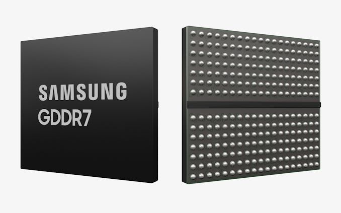

Now that JEDEC has published specification of GDDR7 memory, memory manufacturers are beginning to announce their initial products. The first out of the gate for this generation is Samsung, which has has quietly added its GDDR7 products to its official product catalog.
For now, Samsung lists two GDDR7 devices on its website: 16 Gbit chips rated for an up to 28 GT/s data transfer rate and a faster version running at up to 32 GT/s data transfer rate (which is in line with initial parts that Samsung announced in mid-2023). The chips feature a 512M x32 organization and come in a 266-pin FBGA packaging. The chips are already sampling, so Samsung's customers – GPU vendors, AI inference vendors, network product vendors, and the like – should already have GDDR7 chips in their labs.
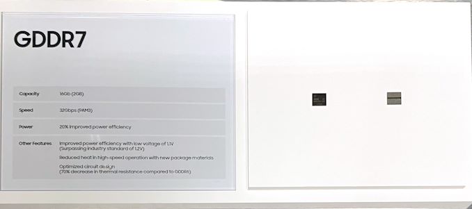
The GDDR7 specification promises the maximum per-chip capacity of 64 Gbit (8 GB) and data transfer rates of 48 GT/s. Meanwhile, first generation GDDR7 chips (as announced so far) will feature a rather moderate capacity of 16 Gbit (2 GB) and a data transfer rate of up to 32 GT/s.
Performance-wise, the first generation of GDDR7 should provide a significant improvement in memory bandwidth over GDDR6 and GDDR6X. However capacity/density improvements will not come until memory manufacturers move to their next generation EUV-based process nodes. As a result, the first GDDR7-based graphics cards are unlikely to sport any memory capacity improvements. Though looking a bit farther down the road, Samsung and SK Hynix have previously told Tom's Hardware that they intend to reach mass production of 24 Gbit GDDR7 chips in 2025.
Otherwise, it is noteworthy that SK Hynix also demonstrated its GDDR7 chips at NVIDIA's GTC last week. So Samsung's competition should be close behind in delivering samples, and eventually mass production memory.
Source: Samsung (via @harukaze5719)
Memory

Demand for high-performance processors for AI training is skyrocketing, and consequently so is the demand for the components that go into these processors. So much so that SK hynix this week is very publicly announcing that the company's high-bandwidth memory (HBM) production capacity has already sold out for the rest of 2024, and even most of 2025 has already sold out as well.
SK hynix currently produces various types of HBM memory for customers like Amazon, AMD, Facebook, Google (Broadcom), Intel, Microsoft, and, of course, NVIDIA. The latter is an especially prolific consumer of HBM3 and HBM3E memory for its H100/H200/GH200 accelerators, as NVIDIA is also working to fill what remains an insatiable (and unmet) demand for its accelerators.
As a result, HBM memory orders, which are already placed months in advance, are now backlogging well into 2025 as chip vendors look to secure supplies of the memory stacks critical to their success.
This has made SK hynix the secnd HBM memory vendor in recent months to announce that they've sold out into 2025, following an earlier announcement from Micron regarding its HBM3E production. But of the two announcements, SK hynix's is arguably the most significant yet, as the South Korean firm's HBM production capacity is far greater than Micron's. So while things were merely "interesting" with the smallest of the Big Three memory manufacturers being sold out into 2025, things are taking a more concerning (and constrained) outlook now that SK hynix is as well.
SK hynix currently controls roughly 46% - 49% of HBM market, and its share is not expected to drop significantly in 2025, according to market tracking firm TrendForce. By contrast, Micron's share on HBM memory market is between 4% and 6%. Since HBM supply of both companies is sold out through the most of 2025, we're likely looking at a scenario where over 50% of the industry's total HBM3/HBM3E supply for the coming quarters is already sold out.
This leaves Samsung as the only member of the group not to comment on HBM demand so far. Though with memory being a highly fungible commodity product, it would be surprising if Samsung wasn't facing similar demand. And, ultimately, all of this is pointing towards the indusry entering an HBM3 memory shortage.
Separately, SK hynix said that it is sampling 12-Hi 36GB HBM3E stacks with customers and will begin volume shipments in the third quarter.
Memory
Lorem Ipsum is simply dummy text of the printing and typesetting industry. Lorem Ipsum has been the industry's.
Demand for high-performance processors for AI training is skyrocketing, and consequently so is the demand for the components that go into these processors. So much so that SK hynix this week is very publicly announcing that the company's high-bandwidth memory (HBM) production capacity has already sold out for the rest of 2024, and even most of 2025 has already sold out as well.
SK hynix currently produces various types of HBM memory for customers like Amazon, AMD, Facebook, Google (Broadcom), Intel, Microsoft, and, of course, NVIDIA. The latter is an especially prolific consumer of HBM3 and HBM3E memory for its H100/H200/GH200 accelerators, as NVIDIA is also working to fill what remains an insatiable (and unmet) demand for its accelerators.
As a result, HBM memory orders, which are already placed months in advance, are now backlogging well into 2025 as chip vendors look to secure supplies of the memory stacks critical to their success.
This has made SK hynix the secnd HBM memory vendor in recent months to announce that they've sold out into 2025, following an earlier announcement from Micron regarding its HBM3E production. But of the two announcements, SK hynix's is arguably the most significant yet, as the South Korean firm's HBM production capacity is far greater than Micron's. So while things were merely "interesting" with the smallest of the Big Three memory manufacturers being sold out into 2025, things are taking a more concerning (and constrained) outlook now that SK hynix is as well.
SK hynix currently controls roughly 46% - 49% of HBM market, and its share is not expected to drop significantly in 2025, according to market tracking firm TrendForce. By contrast, Micron's share on HBM memory market is between 4% and 6%. Since HBM supply of both companies is sold out through the most of 2025, we're likely looking at a scenario where over 50% of the industry's total HBM3/HBM3E supply for the coming quarters is already sold out.
This leaves Samsung as the only member of the group not to comment on HBM demand so far. Though with memory being a highly fungible commodity product, it would be surprising if Samsung wasn't facing similar demand. And, ultimately, all of this is pointing towards the indusry entering an HBM3 memory shortage.
Separately, SK hynix said that it is sampling 12-Hi 36GB HBM3E stacks with customers and will begin volume shipments in the third quarter.
Memory


. The chips feature a 512M x32 organization and come in a 266-pin FBGA packaging. The chips are already sampling, so Samsung's customers – GPU vendors, AI inference vendors, network product vendors, and the like – should already have GDDR7 chips in their labs.</p>
<p>The GDDR7 specification promises the maximum per-chip capacity of 64 Gbit (8 GB) and data transfer rates of 48 GT/s. Meanwhile, first generation GDDR7 chips (as announced so far) will feature a rather moderate capacity of 16 Gbit (2 GB) and a data transfer rate of up to 32 GT/s.</p>
<p align="center"><a href="https://www.anandtech.com/show/21326/samsung-lists-gddr7-memory-chips-on-its-website"><img alt="" src="https://images.anandtech.com/doci/21326/Samsung_GDDR7_GTC_575px.jpg" /></a></p>
<p>Performance-wise, the first generation of GDDR7 should provide a significant improvement in memory bandwidth over GDDR6 and GDDR6X. However capacity/density improvements will not come until memory manufacturers move to their next generation EUV-based process nodes. As a result, the first GDDR7-based graphics cards are unlikely to sport any memory capacity improvements. Though looking a bit farther down the road, Samsung and SK Hynix have previously told <a href="https://www.tomshardware.com/pc-components/gpus/next-gen-gpus-likely-arriving-in-late-2024-with-gddr7-memory-samsung-and-sk-hynix-chips-showed-chips-at-gtc">Tom's Hardware</a> that they intend to reach mass production of 24 Gbit GDDR7 chips in 2025.</p>
<p>Otherwise, it is noteworthy that SK Hynix also demonstrated its GDDR7 chips at NVIDIA's GTC last week. So Samsung's competition should be close behind in delivering samples, and eventually mass production memory.</p>
<p>Source: <a href="https://semiconductor.samsung.com/dram/gddr/gddr7/k4vaf325zc-sc32/">Samsung</a> (via <a href="https://twitter.com/harukaze5719/status/1772512885174120909">@harukaze5719</a>)</p>
</p> Memory)
. The chips feature a 512M x32 organization and come in a 266-pin FBGA packaging. The chips are already sampling, so Samsung's customers – GPU vendors, AI inference vendors, network product vendors, and the like – should already have GDDR7 chips in their labs.</p>
<p>The GDDR7 specification promises the maximum per-chip capacity of 64 Gbit (8 GB) and data transfer rates of 48 GT/s. Meanwhile, first generation GDDR7 chips (as announced so far) will feature a rather moderate capacity of 16 Gbit (2 GB) and a data transfer rate of up to 32 GT/s.</p>
<p align="center"><a href="https://www.anandtech.com/show/21326/samsung-lists-gddr7-memory-chips-on-its-website"><img alt="" src="https://images.anandtech.com/doci/21326/Samsung_GDDR7_GTC_575px.jpg" /></a></p>
<p>Performance-wise, the first generation of GDDR7 should provide a significant improvement in memory bandwidth over GDDR6 and GDDR6X. However capacity/density improvements will not come until memory manufacturers move to their next generation EUV-based process nodes. As a result, the first GDDR7-based graphics cards are unlikely to sport any memory capacity improvements. Though looking a bit farther down the road, Samsung and SK Hynix have previously told <a href="https://www.tomshardware.com/pc-components/gpus/next-gen-gpus-likely-arriving-in-late-2024-with-gddr7-memory-samsung-and-sk-hynix-chips-showed-chips-at-gtc">Tom's Hardware</a> that they intend to reach mass production of 24 Gbit GDDR7 chips in 2025.</p>
<p>Otherwise, it is noteworthy that SK Hynix also demonstrated its GDDR7 chips at NVIDIA's GTC last week. So Samsung's competition should be close behind in delivering samples, and eventually mass production memory.</p>
<p>Source: <a href="https://semiconductor.samsung.com/dram/gddr/gddr7/k4vaf325zc-sc32/">Samsung</a> (via <a href="https://twitter.com/harukaze5719/status/1772512885174120909">@harukaze5719</a>)</p>
</p> Memory | https://compbuddey.blogspot.com/2024/04/gddr7-approaches-samsung-lists-gddr7_49.html)
. The chips feature a 512M x32 organization and come in a 266-pin FBGA packaging. The chips are already sampling, so Samsung's customers – GPU vendors, AI inference vendors, network product vendors, and the like – should already have GDDR7 chips in their labs.</p>
<p>The GDDR7 specification promises the maximum per-chip capacity of 64 Gbit (8 GB) and data transfer rates of 48 GT/s. Meanwhile, first generation GDDR7 chips (as announced so far) will feature a rather moderate capacity of 16 Gbit (2 GB) and a data transfer rate of up to 32 GT/s.</p>
<p align="center"><a href="https://www.anandtech.com/show/21326/samsung-lists-gddr7-memory-chips-on-its-website"><img alt="" src="https://images.anandtech.com/doci/21326/Samsung_GDDR7_GTC_575px.jpg" /></a></p>
<p>Performance-wise, the first generation of GDDR7 should provide a significant improvement in memory bandwidth over GDDR6 and GDDR6X. However capacity/density improvements will not come until memory manufacturers move to their next generation EUV-based process nodes. As a result, the first GDDR7-based graphics cards are unlikely to sport any memory capacity improvements. Though looking a bit farther down the road, Samsung and SK Hynix have previously told <a href="https://www.tomshardware.com/pc-components/gpus/next-gen-gpus-likely-arriving-in-late-2024-with-gddr7-memory-samsung-and-sk-hynix-chips-showed-chips-at-gtc">Tom's Hardware</a> that they intend to reach mass production of 24 Gbit GDDR7 chips in 2025.</p>
<p>Otherwise, it is noteworthy that SK Hynix also demonstrated its GDDR7 chips at NVIDIA's GTC last week. So Samsung's competition should be close behind in delivering samples, and eventually mass production memory.</p>
<p>Source: <a href="https://semiconductor.samsung.com/dram/gddr/gddr7/k4vaf325zc-sc32/">Samsung</a> (via <a href="https://twitter.com/harukaze5719/status/1772512885174120909">@harukaze5719</a>)</p>
</p> Memory&body=https://compbuddey.blogspot.com/2024/04/gddr7-approaches-samsung-lists-gddr7_49.html)
0 Comments