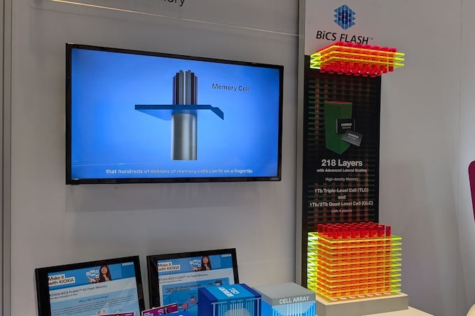

Kioxia's booth at FMS 2024 was a busy one with multiple technology demonstrations keeping visitors occupied. A walk-through of the BiCS 8 manufacturing process was the first to grab my attention. Kioxia and Western Digital announced the sampling of BiCS 8 in March 2023. We had touched briefly upon its CMOS Bonded Array (CBA) scheme in our coverage of Kioxial's 2Tb QLC NAND device and coverage of Western Digital's 128 TB QLC enterprise SSD proof-of-concept demonstration. At Kioxia's booth, we got more insights.
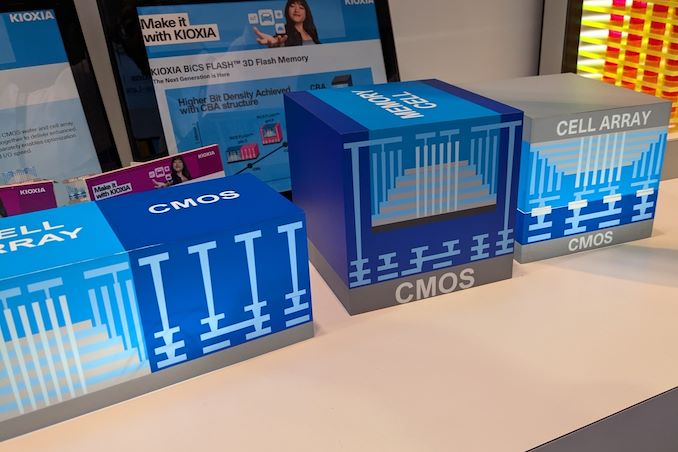
Traditionally, fabrication of flash chips involved placement of the associate logic circuitry (CMOS process) around the periphery of the flash array. The process then moved on to putting the CMOS under the cell array, but the wafer development process was serialized with the CMOS logic getting fabricated first followed by the cell array on top. However, this has some challenges because the cell array requires a high-temperature processing step to ensure higher reliability that can be detrimental to the health of the CMOS logic. Thanks to recent advancements in wafer bonding techniques, the new CBA process allows the CMOS wafer and cell array wafer to be processed independently in parallel and then pieced together, as shown in the models above.
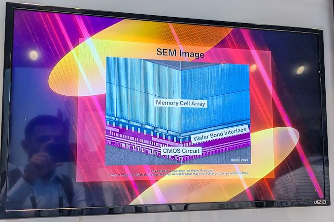
The BiCS 8 3D NAND incorporates 218 layers, compared to 112 layers in BiCS 5 and 162 layers in BiCS 6. The company decided to skip over BiCS 7 (or, rather, it was probably a short-lived generation meant as an internal test vehicle). The generation retains the four-plane charge trap structure of BiCS 6. In its TLC avatar, it is available as a 1 Tbit device. The QLC version is available in two capacities - 1 Tbit and 2 Tbit.
Kioxia also noted that while the number of layers (218) doesn't compare favorably with the latest layer counts from the competition, its lateral scaling / cell shrinkage has enabled it to be competitive in terms of bit density as well as operating speeds (3200 MT/s). For reference, the latest shipping NAND from Micron - the G9 - has 276 layers with a bit density in TLC mode of 21 Gbit/mm2, and operates at up to 3600 MT/s. However, its 232L NAND operates only up to 2400 MT/s and has a bit density of 14.6 Gbit/mm2.
It must be noted that the CBA hybrid bonding process has advantages over the current processes used by other vendors - including Micron's CMOS under array (CuA) and SK hynix's 4D PUC (periphery-under-chip) developed in the late 2010s. It is expected that other NAND vendors will also move eventually to some variant of the hybrid bonding scheme used by Kioxia.
Storage

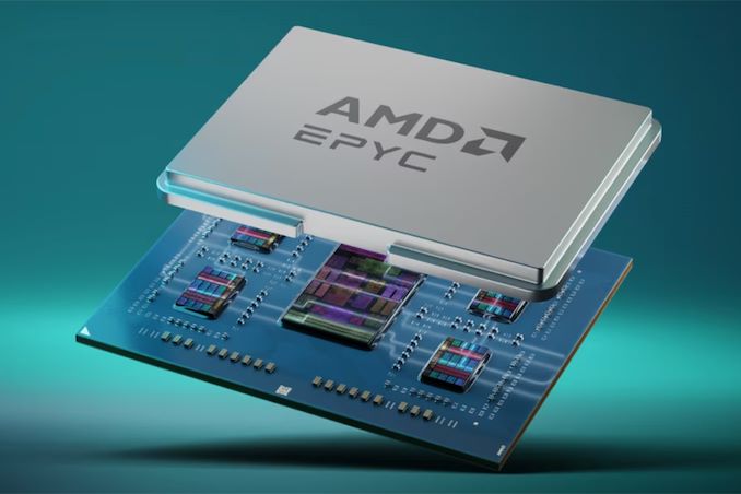
As part of AMD's Q1'2024 earnings announcement this week, the company is offering a brief status update on some of their future products set to launch later this year. Most important among these is an update on their Zen 5 CPU architecture, which is expected to launch for both client and server products later this year.
Highlighting their progress so far, AMD is confirming that EPYC "Turin" processors have begun sampling, and that these early runs of AMD's next-gen datacenter chips are meeting the company's expectations.
"Looking ahead, we are very excited about our next-gen Turin family of EPYC processors featuring our Zen 5 core," said Lisa Su, chief executive officer of AMD, at the conference call with analysts and investors (via SeekingAlpha). "We are widely sampling Turin, and the silicon is looking great. In the cloud, the significant performance and efficiency increases of Turin position us well to capture an even larger share of both first and third-party workloads."
Overall, it looks like AMD is on-track to solidify its position, and perhaps even increase its datacenter market share with its EPYC Turin processors. According to AMD, the company's server partners are developing a 30% larger number of designs for Turin than they did Genoa. This underscores how AMD's partners are preparing for even more market share growth on the back of AMD's ongoing success, not to mention the improved performance and power efficiency that the Zen 5 architecture should offer.
"In addition, there are 30% more Turin platforms in development from our server partners, compared to 4th Generation EPYC platforms, increasing our enterprise and with new solutions optimized for additional workloads," Su said. "Turin remains on track to launch later this year."
AMD's EPYC 'Turin' processors will be drop-in compatible with existing SP5 platforms (i.e., will come in an LGA 6096 package), which will facilitate its faster ramp and adoption of the platform both by cloud giants and server makers. In addition, AMD's next-generation EPYC CPUs are expected to feature more than 96 cores and a more versatile memory subsystem.
CPUs
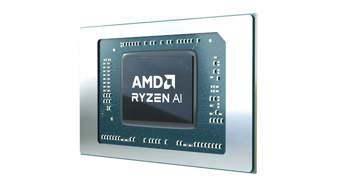
In what appears to be a mistake or a jump of the gun by ASUS, they have seemingly published a list of specifications for one of its key notebooks that all but allude to the next generation of AMD's mobile processors. While we saw AMD toy with a new nomenclature for their Phoenix silicon (Ryzen 7040 series), it seems as though AMD is once again changing things around where their naming scheme for processors is concerned.
The ASUS listing, which has now since been deleted, but as of writing is still available through Google's cache, highlights a model that is already in existence, the VivoBook S 16 OLED (M5606), but is listed with an unknown AMD Ryzen AI 9 HX 170 processor. Which, based on its specificiations, is certainly not part of the current Hawk Point (Phoenix/Phoenix 2) platform.
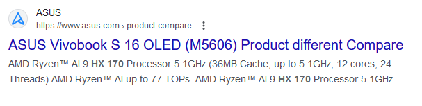
The cache on Google shows the ASUS Vivobook S 16 OLED with a Ryzen AI 9 HX 170 Processor
While it does happen in this industry occasionally, what looks like an accidental leak by ASUS on one of their product pages has unearthed an unknown processor from AMD. This first came to our attention via a post on Twitter by user @harukaze5719. While we don't speculate on rumors, we confirmed this ourselves by digging through Google's cache. Sure enough, as the image above from Google highlights, it lists a newly unannounced model of Ryzen mobile processor. Under the listing via the product compare section for the ASUS Vivobook S 16 OLED (M5606) notebook, it is listed with the AMD Ryzen AI 9 HX 170, which appears to be one of AMD's upcoming Zen 5-based mobile chips codenamed Strix Point.
So with the seemingly new nomenclature that AMD has gone with, it has a clear focus on AI, or rather Ryzen AI, by including it in the name. The Ryzen AI 9 HX 170 looks set to be a 12C/24T Zen 5 mobile variant, with their Ryzen AI NPU or similar integrated within the chip. Given that Microsoft has defined that only processors with an NPU with 45 TOPS of performance or over constitute being considered an 'AI PC', it's likely the Xilinx (now AMD Xilinx) based NPU will meet these requirements as the listing states the chip has up to 77 TOPS of AI performance available. The HX series is strikingly similar to AMD's (and Intel's) previous HX naming series for their desktop replacement SKUs for laptops, so assuming any of the details of ASUS's error are correct, then this is presumably a very high-end, high-TDP part.
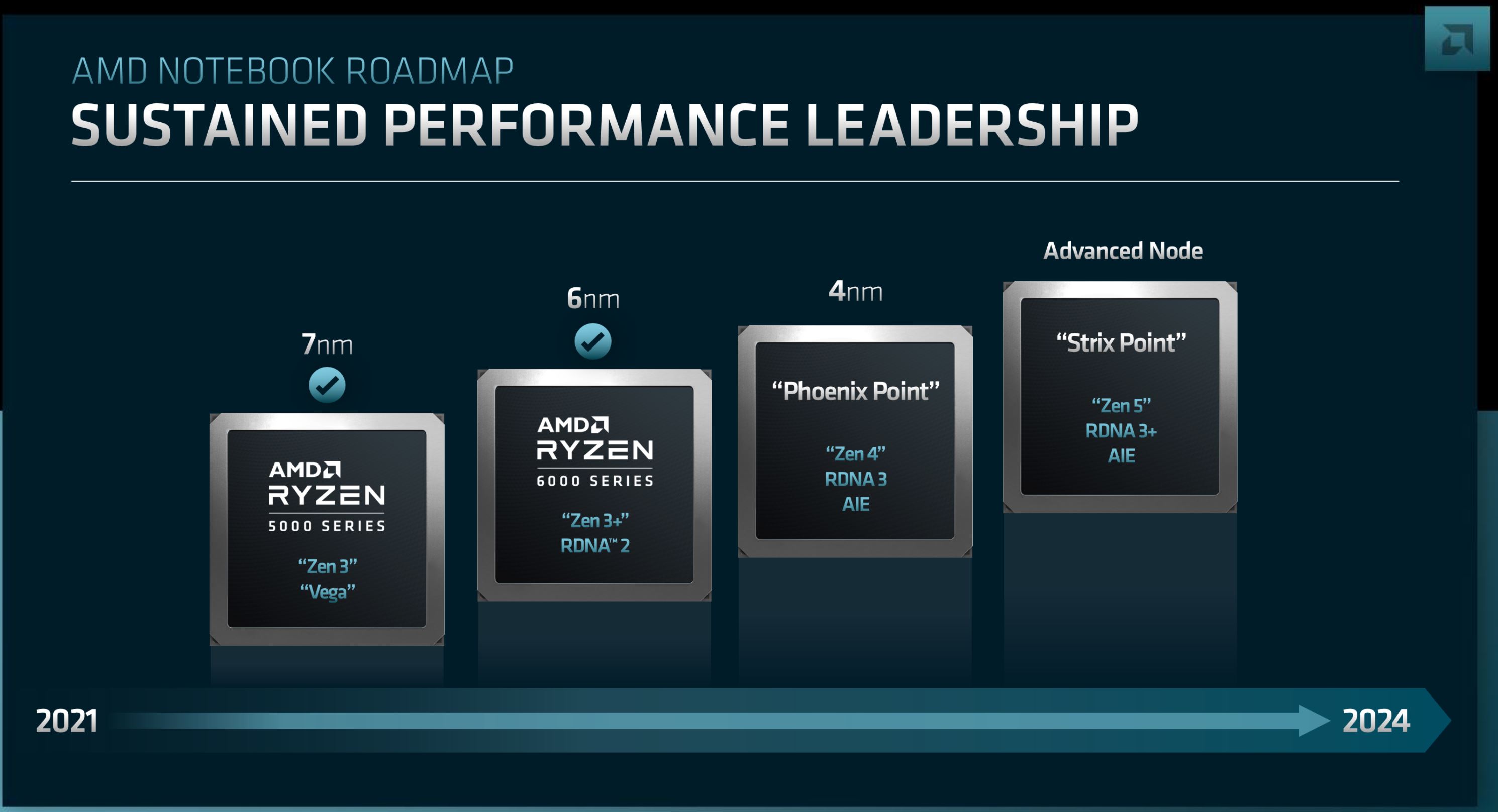
AMD Laptop Roadmap from Zen 2 in 2019 to Zen 5 on track for release in 2024
We've known for some time that AMD plans to release AMD's Zen 5-based Strix Point line-up sometime in 2024. Given the timing of Computex 2024, which is just over four weeks away, we still don't quite have the full picture of Zen 5's performance and its architectural shift over Zen 4. AMD CEO Dr. Lisa Su also confirmed that Zen 5 will come with enhanced RDNA graphics within the Strix Point SoC by stating "Strix combines our next-gen Zen 5 core with enhanced RDNA graphics and an updated Ryzen AI engine to significantly increase the performance, energy efficiency, and AI capabilities of PCs,"
While it's entirely possible as we lead up to Computex 2024 that AMD is prepared to announce more details about Zen 5, nothing is confirmed. We do know that the CEO of AMD, Dr. Lisa Su is scheduled to deliver the opening keynote of the show, Dr. Lisa Su unveiled their Zen 4 microarchitecture at Computex 2022 during AMD's keynote and even unveiled their 3D V-Cache stacking, which we know today as the Ryzen X3D CPUs back at Computex 2021.
With that in mind, AMD and Dr. Lisa Su love to announce new products and ... CPUs

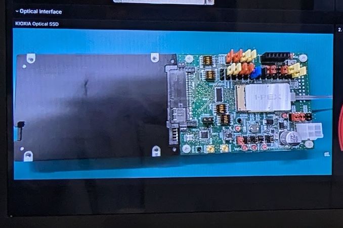
A few years back, the Japanese government's New Energy and Industrial Technology Development Organization (NEDO ) allocated funding for the development of green datacenter technologies. With the aim to obtain up to 40% savings in overall power consumption, several Japanese companies have been developing an optical interface for their enterprise SSDs. And at this year's FMS, Kioxia had their optical interface on display.
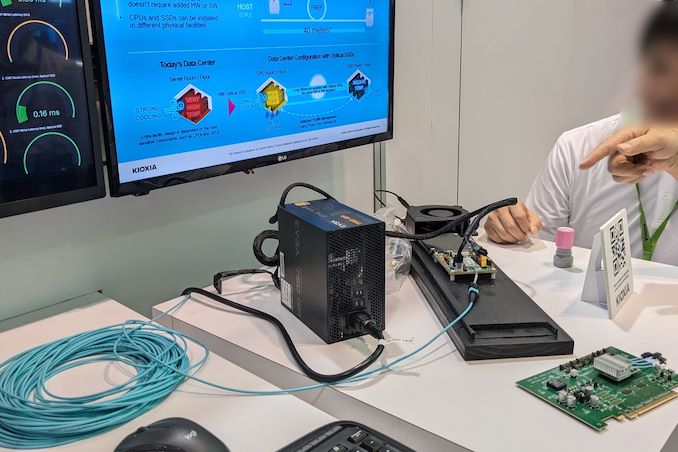
For this demonstration, Kioxia took its existing CM7 enterprise SSD and created an optical interface for it. A PCIe card with on-board optics developed by Kyocera is installed in the server slot. An optical interface allows data transfer over long distances (it was 40m in the demo, but Kioxia promises lengths of up to 100m for the cable in the future). This allows the storage to be kept in a separate room with minimal cooling requirements compared to the rack with the CPUs and GPUs. Disaggregation of different server components will become an option as very high throughput interfaces such as PCIe 7.0 (with 128 GT/s rates) become available.
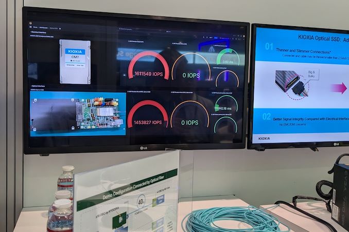
The demonstration of the optical SSD showed a slight loss in IOPS performance, but a significant advantage in the latency metric over the shipping enterprise SSD behind a copper network link. Obviously, there are advantages in wiring requirements and signal integrity maintenance with optical links.
Being a proof-of-concept demonstration, we do see the requirement for an industry-standard approach if this were to gain adoption among different datacenter vendors. The PCI-SIG optical workgroup will need to get its act together soon to create a standards-based approach to this problem.
Storage
As part of AMD's Q1'2024 earnings announcement this week, the company is offering a brief status update on some of their future products set to launch later this year. Most important among these is an update on their Zen 5 CPU architecture, which is expected to launch for both client and server products later this year.
Highlighting their progress so far, AMD is confirming that EPYC "Turin" processors have begun sampling, and that these early runs of AMD's next-gen datacenter chips are meeting the company's expectations.
"Looking ahead, we are very excited about our next-gen Turin family of EPYC processors featuring our Zen 5 core," said Lisa Su, chief executive officer of AMD, at the conference call with analysts and investors (via SeekingAlpha). "We are widely sampling Turin, and the silicon is looking great. In the cloud, the significant performance and efficiency increases of Turin position us well to capture an even larger share of both first and third-party workloads."
Overall, it looks like AMD is on-track to solidify its position, and perhaps even increase its datacenter market share with its EPYC Turin processors. According to AMD, the company's server partners are developing a 30% larger number of designs for Turin than they did Genoa. This underscores how AMD's partners are preparing for even more market share growth on the back of AMD's ongoing success, not to mention the improved performance and power efficiency that the Zen 5 architecture should offer.
"In addition, there are 30% more Turin platforms in development from our server partners, compared to 4th Generation EPYC platforms, increasing our enterprise and with new solutions optimized for additional workloads," Su said. "Turin remains on track to launch later this year."
AMD's EPYC 'Turin' processors will be drop-in compatible with existing SP5 platforms (i.e., will come in an LGA 6096 package), which will facilitate its faster ramp and adoption of the platform both by cloud giants and server makers. In addition, AMD's next-generation EPYC CPUs are expected to feature more than 96 cores and a more versatile memory subsystem.
CPUs
As part of AMD's Q1'2024 earnings announcement this week, the company is offering a brief status update on some of their future products set to launch later this year. Most important among these is an update on their Zen 5 CPU architecture, which is expected to launch for both client and server products later this year.
Highlighting their progress so far, AMD is confirming that EPYC "Turin" processors have begun sampling, and that these early runs of AMD's next-gen datacenter chips are meeting the company's expectations.
"Looking ahead, we are very excited about our next-gen Turin family of EPYC processors featuring our Zen 5 core," said Lisa Su, chief executive officer of AMD, at the conference call with analysts and investors (via SeekingAlpha). "We are widely sampling Turin, and the silicon is looking great. In the cloud, the significant performance and efficiency increases of Turin position us well to capture an even larger share of both first and third-party workloads."
Overall, it looks like AMD is on-track to solidify its position, and perhaps even increase its datacenter market share with its EPYC Turin processors. According to AMD, the company's server partners are developing a 30% larger number of designs for Turin than they did Genoa. This underscores how AMD's partners are preparing for even more market share growth on the back of AMD's ongoing success, not to mention the improved performance and power efficiency that the Zen 5 architecture should offer.
"In addition, there are 30% more Turin platforms in development from our server partners, compared to 4th Generation EPYC platforms, increasing our enterprise and with new solutions optimized for additional workloads," Su said. "Turin remains on track to launch later this year."
AMD's EPYC 'Turin' processors will be drop-in compatible with existing SP5 platforms (i.e., will come in an LGA 6096 package), which will facilitate its faster ramp and adoption of the platform both by cloud giants and server makers. In addition, AMD's next-generation EPYC CPUs are expected to feature more than 96 cores and a more versatile memory subsystem.
CPUs
In what appears to be a mistake or a jump of the gun by ASUS, they have seemingly published a list of specifications for one of its key notebooks that all but allude to the next generation of AMD's mobile processors. While we saw AMD toy with a new nomenclature for their Phoenix silicon (Ryzen 7040 series), it seems as though AMD is once again changing things around where their naming scheme for processors is concerned.
The ASUS listing, which has now since been deleted, but as of writing is still available through Google's cache, highlights a model that is already in existence, the VivoBook S 16 OLED (M5606), but is listed with an unknown AMD Ryzen AI 9 HX 170 processor. Which, based on its specificiations, is certainly not part of the current Hawk Point (Phoenix/Phoenix 2) platform.
The cache on Google shows the ASUS Vivobook S 16 OLED with a Ryzen AI 9 HX 170 Processor
While it does happen in this industry occasionally, what looks like an accidental leak by ASUS on one of their product pages has unearthed an unknown processor from AMD. This first came to our attention via a post on Twitter by user @harukaze5719. While we don't speculate on rumors, we confirmed this ourselves by digging through Google's cache. Sure enough, as the image above from Google highlights, it lists a newly unannounced model of Ryzen mobile processor. Under the listing via the product compare section for the ASUS Vivobook S 16 OLED (M5606) notebook, it is listed with the AMD Ryzen AI 9 HX 170, which appears to be one of AMD's upcoming Zen 5-based mobile chips codenamed Strix Point.
So with the seemingly new nomenclature that AMD has gone with, it has a clear focus on AI, or rather Ryzen AI, by including it in the name. The Ryzen AI 9 HX 170 looks set to be a 12C/24T Zen 5 mobile variant, with their Ryzen AI NPU or similar integrated within the chip. Given that Microsoft has defined that only processors with an NPU with 45 TOPS of performance or over constitute being considered an 'AI PC', it's likely the Xilinx (now AMD Xilinx) based NPU will meet these requirements as the listing states the chip has up to 77 TOPS of AI performance available. The HX series is strikingly similar to AMD's (and Intel's) previous HX naming series for their desktop replacement SKUs for laptops, so assuming any of the details of ASUS's error are correct, then this is presumably a very high-end, high-TDP part.
AMD Laptop Roadmap from Zen 2 in 2019 to Zen 5 on track for release in 2024
We've known for some time that AMD plans to release AMD's Zen 5-based Strix Point line-up sometime in 2024. Given the timing of Computex 2024, which is just over four weeks away, we still don't quite have the full picture of Zen 5's performance and its architectural shift over Zen 4. AMD CEO Dr. Lisa Su also confirmed that Zen 5 will come with enhanced RDNA graphics within the Strix Point SoC by stating "Strix combines our next-gen Zen 5 core with enhanced RDNA graphics and an updated Ryzen AI engine to significantly increase the performance, energy efficiency, and AI capabilities of PCs,"
While it's entirely possible as we lead up to Computex 2024 that AMD is prepared to announce more details about Zen 5, nothing is confirmed. We do know that the CEO of AMD, Dr. Lisa Su is scheduled to deliver the opening keynote of the show, Dr. Lisa Su unveiled their Zen 4 microarchitecture at Computex 2022 during AMD's keynote and even unveiled their 3D V-Cache stacking, which we know today as the Ryzen X3D CPUs back at Computex 2021.
With that in mind, AMD and Dr. Lisa Su love to announce new products and ... CPUs
A few years back, the Japanese government's New Energy and Industrial Technology Development Organization (NEDO ) allocated funding for the development of green datacenter technologies. With the aim to obtain up to 40% savings in overall power consumption, several Japanese companies have been developing an optical interface for their enterprise SSDs. And at this year's FMS, Kioxia had their optical interface on display.
For this demonstration, Kioxia took its existing CM7 enterprise SSD and created an optical interface for it. A PCIe card with on-board optics developed by Kyocera is installed in the server slot. An optical interface allows data transfer over long distances (it was 40m in the demo, but Kioxia promises lengths of up to 100m for the cable in the future). This allows the storage to be kept in a separate room with minimal cooling requirements compared to the rack with the CPUs and GPUs. Disaggregation of different server components will become an option as very high throughput interfaces such as PCIe 7.0 (with 128 GT/s rates) become available.
The demonstration of the optical SSD showed a slight loss in IOPS performance, but a significant advantage in the latency metric over the shipping enterprise SSD behind a copper network link. Obviously, there are advantages in wiring requirements and signal integrity maintenance with optical links.
Being a proof-of-concept demonstration, we do see the requirement for an industry-standard approach if this were to gain adoption among different datacenter vendors. The PCI-SIG optical workgroup will need to get its act together soon to create a standards-based approach to this problem.
Storage
As part of AMD's Q1'2024 earnings announcement this week, the company is offering a brief status update on some of their future products set to launch later this year. Most important among these is an update on their Zen 5 CPU architecture, which is expected to launch for both client and server products later this year.
Highlighting their progress so far, AMD is confirming that EPYC "Turin" processors have begun sampling, and that these early runs of AMD's next-gen datacenter chips are meeting the company's expectations.
"Looking ahead, we are very excited about our next-gen Turin family of EPYC processors featuring our Zen 5 core," said Lisa Su, chief executive officer of AMD, at the conference call with analysts and investors (via SeekingAlpha). "We are widely sampling Turin, and the silicon is looking great. In the cloud, the significant performance and efficiency increases of Turin position us well to capture an even larger share of both first and third-party workloads."
Overall, it looks like AMD is on-track to solidify its position, and perhaps even increase its datacenter market share with its EPYC Turin processors. According to AMD, the company's server partners are developing a 30% larger number of designs for Turin than they did Genoa. This underscores how AMD's partners are preparing for even more market share growth on the back of AMD's ongoing success, not to mention the improved performance and power efficiency that the Zen 5 architecture should offer.
"In addition, there are 30% more Turin platforms in development from our server partners, compared to 4th Generation EPYC platforms, increasing our enterprise and with new solutions optimized for additional workloads," Su said. "Turin remains on track to launch later this year."
AMD's EPYC 'Turin' processors will be drop-in compatible with existing SP5 platforms (i.e., will come in an LGA 6096 package), which will facilitate its faster ramp and adoption of the platform both by cloud giants and server makers. In addition, AMD's next-generation EPYC CPUs are expected to feature more than 96 cores and a more versatile memory subsystem.
CPUs
A few years back, the Japanese government's New Energy and Industrial Technology Development Organization (NEDO ) allocated funding for the development of green datacenter technologies. With the aim to obtain up to 40% savings in overall power consumption, several Japanese companies have been developing an optical interface for their enterprise SSDs. And at this year's FMS, Kioxia had their optical interface on display.
For this demonstration, Kioxia took its existing CM7 enterprise SSD and created an optical interface for it. A PCIe card with on-board optics developed by Kyocera is installed in the server slot. An optical interface allows data transfer over long distances (it was 40m in the demo, but Kioxia promises lengths of up to 100m for the cable in the future). This allows the storage to be kept in a separate room with minimal cooling requirements compared to the rack with the CPUs and GPUs. Disaggregation of different server components will become an option as very high throughput interfaces such as PCIe 7.0 (with 128 GT/s rates) become available.
The demonstration of the optical SSD showed a slight loss in IOPS performance, but a significant advantage in the latency metric over the shipping enterprise SSD behind a copper network link. Obviously, there are advantages in wiring requirements and signal integrity maintenance with optical links.
Being a proof-of-concept demonstration, we do see the requirement for an industry-standard approach if this were to gain adoption among different datacenter vendors. The PCI-SIG optical workgroup will need to get its act together soon to create a standards-based approach to this problem.
Storage
A few years back, the Japanese government's New Energy and Industrial Technology Development Organization (NEDO ) allocated funding for the development of green datacenter technologies. With the aim to obtain up to 40% savings in overall power consumption, several Japanese companies have been developing an optical interface for their enterprise SSDs. And at this year's FMS, Kioxia had their optical interface on display.
For this demonstration, Kioxia took its existing CM7 enterprise SSD and created an optical interface for it. A PCIe card with on-board optics developed by Kyocera is installed in the server slot. An optical interface allows data transfer over long distances (it was 40m in the demo, but Kioxia promises lengths of up to 100m for the cable in the future). This allows the storage to be kept in a separate room with minimal cooling requirements compared to the rack with the CPUs and GPUs. Disaggregation of different server components will become an option as very high throughput interfaces such as PCIe 7.0 (with 128 GT/s rates) become available.
The demonstration of the optical SSD showed a slight loss in IOPS performance, but a significant advantage in the latency metric over the shipping enterprise SSD behind a copper network link. Obviously, there are advantages in wiring requirements and signal integrity maintenance with optical links.
Being a proof-of-concept demonstration, we do see the requirement for an industry-standard approach if this were to gain adoption among different datacenter vendors. The PCI-SIG optical workgroup will need to get its act together soon to create a standards-based approach to this problem.
Storage
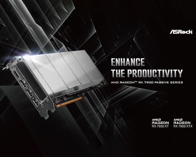
As sales of GPU-based AI accelerators remain as strong as ever, the immense demand for these cards has led to some server builders going off the beaten path in order to get the hardware they want at a lower price. While both NVIDIA and AMD offer official card configurations for servers, the correspondingly high price of these cards makes them a significant financial outlay that some customers either can't afford, or don't want to pay.
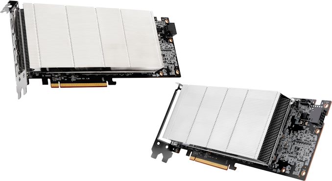
Instead, these groups have been turning to buying up consumer graphics cards, which although they come with additional limitations, are also a fraction of the cost of a "proper" server card. And this week, ASRock has removed another one of those limitations for would-be AMD Radeon users, with the introduction of a set of compact, passively-cooled Radeon RX 7900 XTX and RX 7900 XT video cards that are designed to go in servers.
Without any doubts, ASRock's AMD Radeon RX 7900 XTX Passive 24GB and AMD Radeon RX 7900 XT Passive 20GB AIBs are indeed graphics cards with four display outputs and based on the Navi 31 graphics processor (with 6144 and 5376 stream processors, respectively), so they can output graphics and work both with games and professional applications. And with TGPs of 355W and 315W respectively, these cards aren't underclocked in any way compared to traditional desktop cards. However, unlike a typical desktop card, the cooler on these cards is a dual-slot heatsink without any kind of fan attached, which is meant to be used with high-airflow forced-air cooling.
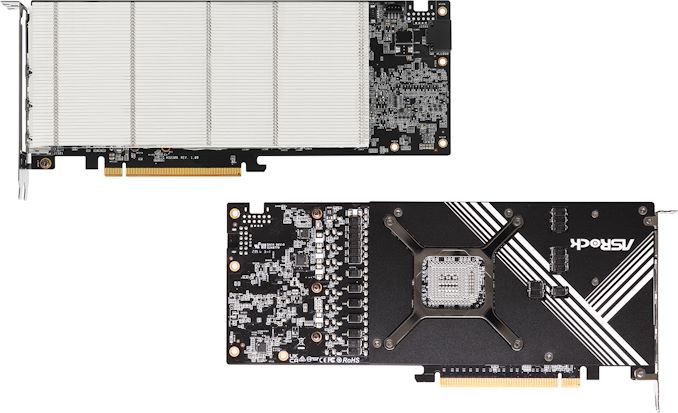
All-told, ASRock's passive cooler is pretty capable, as well; it's not just a simple aluminum heatsink. Beneath the fins, ASRock has gone with a vapor chamber and multiple heat pipes to distribute heat to the rest of the sink. Even with forced-air cooling in racked servers, the heatsink itself still needs to be efficient to keep a 300W+ card cool with only a dual-slot cooler – and especially so when upwards of four of these cards are installed side-by-side with each other. To make the boards even more server friendly, these cards are equipped with a 12V-2×6 power connector, a first for the Radeon RX 7900 series, simplifying installation by reducing cable clutter.
Driving the demand for these cards in particular is their memory configuration. With 24GB for the 7900 XTX and 20GB for the 7900 XT is half as much (or less) memory than can be found on AMD and NVIDIA's high-end professional and server cards, AMD is the only vendor offering consumer cards with this much memory for less than $1000. So for a memory-intensive AI inference cluster built on a low budget, the cheapest 24GB card available starts looking like a tantalizing option.
Otherwise, ASRock's Radeon RX 7900 Passive cards distinguish themselves from AMD's formal professional and server cards by what they're not capable of doing: namely, remote professional graphics or other applications that need things like GPU partitioning. These parts look to be aimed at one application only, artificial intelligence, and are meant to process huge amounts of data. For this purpose, their passive coolers will do the job and the lack of ProViz or VDI-oriented drives ensure that AMD will leave these lucrative markets for itself.
GPUs
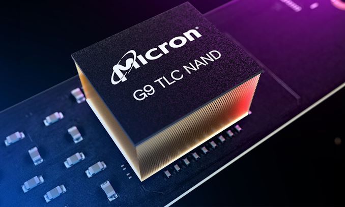
Micron on Tuesday announced that the company has begun shipping its 9th Generation (G9) 276 layer TLC NAND. The next generation of NAND from the prolific memory maker, Micron's latest NAND is designed to further push the envelope on TLC NAND performance, offering significant density and performance improvements over its existing NAND technology.
Micron's G9 TLC NAND memory features 276 active layers, which is up from 232-layers in case of Micron's previous generation TLC NAND. At this point the company is being light on technical details in their official material. However in a brief interview with Blocks & Files, the company confirmed that their 276L NAND still uses a six plane architecture, which was first introduced with the 232L generation. At this point we're assuming Micron is also string-stacking two decks of NAND together, as they have been for the past couple of generations, which means we're looking at 138 layer decks.
| Micron TLC NAND Flash Memory | |||
| 276L | 232L (B58R) |
176L (B47R) |
|
| Layers | 276 | 232 | 176 |
| Decks | 2 (x138)? | 2 (x116) | 2 (x88) |
| Die Capacity | 1 Tbit | 1 Tbit | 512 Gbit |
| Die Size (mm2) | ~48.9mm2 | ~70.1mm2 | ~49.8mm2 |
| Density (Gbit/mm2) | ~21 | 14.6 | 10.3 |
| I/O Speed | 3.6 GT/s (ONFi 5.1) |
2.4 GT/s (ONFi 5.0) |
1.6 GT/s (ONFI 4.2) |
| Planes | 6 | 6 | 4 |
| CuA / PuC | Yes | Yes | Yes |
On the density front, Micron told Blocks & Files that they have improved their NAND density by 44% over their 232L generation. Which, given what we know about that generation, would put the density at around 21 Gbit/mm2. Or for a 1Tbit die of TLC NAND, that works out to a die size of roughly 48.9mm2, comparable to the die size of a 512Gbit TLC die from Micron's older 176L NAND.
Besides improving density, the other big push with Micron's newest generation of NAND was further improving its throughput. While the company's 232L NAND was built against the ONFi 5.0 specification, which topped out at transfer rates of 2400 MT/sec, their new 276L NAND can hit 3600 MT/sec, which is consistent with the ONFi 5.1 spec.
Meanwhile, the eagle-eyed will likely also pick up on Micron's ninth-generation/G9 branding, which is new to the company. Micron's has not previously used this kind of generational branding for their NAND, which up until now has simply been identified by its layer count (and before the 3D era, its feature size). Internally, this is believed to be Micron's 7th generation 3D NAND architecture. However, taking a page from the logic fab industry, Micron seems to be branding it as ninth-generation in order to keep generational parity with its competitors, who are preparing their own 8th/9th generation NAND (and thus cliam that they are the first NAND maker to ship 9th gen NAND).
And while this NAND will eventually end up in ... SSDs

Lorem Ipsum is simply dummy text of the printing and typesetting industry. Lorem Ipsum has been the industry's.
As part of AMD's Q1'2024 earnings announcement this week, the company is offering a brief status update on some of their future products set to launch later this year. Most important among these is an update on their Zen 5 CPU architecture, which is expected to launch for both client and server products later this year.
Highlighting their progress so far, AMD is confirming that EPYC "Turin" processors have begun sampling, and that these early runs of AMD's next-gen datacenter chips are meeting the company's expectations.
"Looking ahead, we are very excited about our next-gen Turin family of EPYC processors featuring our Zen 5 core," said Lisa Su, chief executive officer of AMD, at the conference call with analysts and investors (via SeekingAlpha). "We are widely sampling Turin, and the silicon is looking great. In the cloud, the significant performance and efficiency increases of Turin position us well to capture an even larger share of both first and third-party workloads."
Overall, it looks like AMD is on-track to solidify its position, and perhaps even increase its datacenter market share with its EPYC Turin processors. According to AMD, the company's server partners are developing a 30% larger number of designs for Turin than they did Genoa. This underscores how AMD's partners are preparing for even more market share growth on the back of AMD's ongoing success, not to mention the improved performance and power efficiency that the Zen 5 architecture should offer.
"In addition, there are 30% more Turin platforms in development from our server partners, compared to 4th Generation EPYC platforms, increasing our enterprise and with new solutions optimized for additional workloads," Su said. "Turin remains on track to launch later this year."
AMD's EPYC 'Turin' processors will be drop-in compatible with existing SP5 platforms (i.e., will come in an LGA 6096 package), which will facilitate its faster ramp and adoption of the platform both by cloud giants and server makers. In addition, AMD's next-generation EPYC CPUs are expected to feature more than 96 cores and a more versatile memory subsystem.
CPUs
In what appears to be a mistake or a jump of the gun by ASUS, they have seemingly published a list of specifications for one of its key notebooks that all but allude to the next generation of AMD's mobile processors. While we saw AMD toy with a new nomenclature for their Phoenix silicon (Ryzen 7040 series), it seems as though AMD is once again changing things around where their naming scheme for processors is concerned.
The ASUS listing, which has now since been deleted, but as of writing is still available through Google's cache, highlights a model that is already in existence, the VivoBook S 16 OLED (M5606), but is listed with an unknown AMD Ryzen AI 9 HX 170 processor. Which, based on its specificiations, is certainly not part of the current Hawk Point (Phoenix/Phoenix 2) platform.
The cache on Google shows the ASUS Vivobook S 16 OLED with a Ryzen AI 9 HX 170 Processor
While it does happen in this industry occasionally, what looks like an accidental leak by ASUS on one of their product pages has unearthed an unknown processor from AMD. This first came to our attention via a post on Twitter by user @harukaze5719. While we don't speculate on rumors, we confirmed this ourselves by digging through Google's cache. Sure enough, as the image above from Google highlights, it lists a newly unannounced model of Ryzen mobile processor. Under the listing via the product compare section for the ASUS Vivobook S 16 OLED (M5606) notebook, it is listed with the AMD Ryzen AI 9 HX 170, which appears to be one of AMD's upcoming Zen 5-based mobile chips codenamed Strix Point.
So with the seemingly new nomenclature that AMD has gone with, it has a clear focus on AI, or rather Ryzen AI, by including it in the name. The Ryzen AI 9 HX 170 looks set to be a 12C/24T Zen 5 mobile variant, with their Ryzen AI NPU or similar integrated within the chip. Given that Microsoft has defined that only processors with an NPU with 45 TOPS of performance or over constitute being considered an 'AI PC', it's likely the Xilinx (now AMD Xilinx) based NPU will meet these requirements as the listing states the chip has up to 77 TOPS of AI performance available. The HX series is strikingly similar to AMD's (and Intel's) previous HX naming series for their desktop replacement SKUs for laptops, so assuming any of the details of ASUS's error are correct, then this is presumably a very high-end, high-TDP part.
AMD Laptop Roadmap from Zen 2 in 2019 to Zen 5 on track for release in 2024
We've known for some time that AMD plans to release AMD's Zen 5-based Strix Point line-up sometime in 2024. Given the timing of Computex 2024, which is just over four weeks away, we still don't quite have the full picture of Zen 5's performance and its architectural shift over Zen 4. AMD CEO Dr. Lisa Su also confirmed that Zen 5 will come with enhanced RDNA graphics within the Strix Point SoC by stating "Strix combines our next-gen Zen 5 core with enhanced RDNA graphics and an updated Ryzen AI engine to significantly increase the performance, energy efficiency, and AI capabilities of PCs,"
While it's entirely possible as we lead up to Computex 2024 that AMD is prepared to announce more details about Zen 5, nothing is confirmed. We do know that the CEO of AMD, Dr. Lisa Su is scheduled to deliver the opening keynote of the show, Dr. Lisa Su unveiled their Zen 4 microarchitecture at Computex 2022 during AMD's keynote and even unveiled their 3D V-Cache stacking, which we know today as the Ryzen X3D CPUs back at Computex 2021.
With that in mind, AMD and Dr. Lisa Su love to announce new products and ... CPUs
A few years back, the Japanese government's New Energy and Industrial Technology Development Organization (NEDO ) allocated funding for the development of green datacenter technologies. With the aim to obtain up to 40% savings in overall power consumption, several Japanese companies have been developing an optical interface for their enterprise SSDs. And at this year's FMS, Kioxia had their optical interface on display.
For this demonstration, Kioxia took its existing CM7 enterprise SSD and created an optical interface for it. A PCIe card with on-board optics developed by Kyocera is installed in the server slot. An optical interface allows data transfer over long distances (it was 40m in the demo, but Kioxia promises lengths of up to 100m for the cable in the future). This allows the storage to be kept in a separate room with minimal cooling requirements compared to the rack with the CPUs and GPUs. Disaggregation of different server components will become an option as very high throughput interfaces such as PCIe 7.0 (with 128 GT/s rates) become available.
The demonstration of the optical SSD showed a slight loss in IOPS performance, but a significant advantage in the latency metric over the shipping enterprise SSD behind a copper network link. Obviously, there are advantages in wiring requirements and signal integrity maintenance with optical links.
Being a proof-of-concept demonstration, we do see the requirement for an industry-standard approach if this were to gain adoption among different datacenter vendors. The PCI-SIG optical workgroup will need to get its act together soon to create a standards-based approach to this problem.
Storage



 scheme in our coverage of Kioxial's <a href="https://www.anandtech.com/show/21464">2Tb QLC NAND device</a> and <a href="https://www.anandtech.com/show/21505">coverage</a> of Western Digital's 128 TB QLC enterprise SSD proof-of-concept demonstration. At Kioxia's booth, we got more insights.</p>
<p align="center"><a href="https://www.anandtech.com/show/21519/kioxia-details-bics-8-at-fms-2024"><img alt="" src="https://images.anandtech.com/doci/21519/bics8-nor-cua-cba_575px.jpg" /></a></p>
<p>Traditionally, fabrication of flash chips involved placement of the associate logic circuitry (CMOS process) around the periphery of the flash array. The process then moved on to putting the CMOS under the cell array, but the wafer development process was serialized with the CMOS logic getting fabricated first followed by the cell array on top. However, this has some challenges because the cell array requires a high-temperature processing step to ensure higher reliability that can be detrimental to the health of the CMOS logic. Thanks to recent advancements in wafer bonding techniques, the new CBA process allows the CMOS wafer and cell array wafer to be processed independently in parallel and then pieced together, as shown in the models above.</p>
<p align="center"><a href="https://www.anandtech.com/show/21519/kioxia-details-bics-8-at-fms-2024"><img alt="" src="https://images.anandtech.com/doci/21519/bica8-cba-sem_575px.jpg" /></a></p>
<p>The BiCS 8 3D NAND incorporates 218 layers, compared to 112 layers in BiCS 5 and 162 layers in BiCS 6. The company decided to skip over BiCS 7 (or, rather, it was probably a short-lived generation meant as an internal test vehicle). The generation retains the four-plane charge trap structure of BiCS 6. In its TLC avatar, it is available as a 1 Tbit device. The QLC version is available in two capacities - 1 Tbit and 2 Tbit.</p>
<p>Kioxia also noted that while the number of layers (218) doesn't compare favorably with the latest layer counts from the competition, its lateral scaling / cell shrinkage has enabled it to be competitive in terms of bit density as well as operating speeds (3200 MT/s). For reference, the latest shipping NAND from Micron - the <a href="https://www.anandtech.com/show/21492">G9</a> - has 276 layers with a bit density in TLC mode of 21 Gbit/mm<sup>2</sup>, and operates at up to 3600 MT/s. However, its 232L NAND operates only up to 2400 MT/s and has a bit density of 14.6 Gbit/mm<sup>2</sup>.</p>
<p>It must be noted that the CBA hybrid bonding process has advantages over the current processes used by other vendors - including Micron's CMOS under array (CuA) and SK hynix's 4D PUC (periphery-under-chip) developed in the late 2010s. It is expected that other NAND vendors will also move eventually to some variant of the hybrid bonding scheme used by Kioxia.</p>
</p> Storage)
 scheme in our coverage of Kioxial's <a href="https://www.anandtech.com/show/21464">2Tb QLC NAND device</a> and <a href="https://www.anandtech.com/show/21505">coverage</a> of Western Digital's 128 TB QLC enterprise SSD proof-of-concept demonstration. At Kioxia's booth, we got more insights.</p>
<p align="center"><a href="https://www.anandtech.com/show/21519/kioxia-details-bics-8-at-fms-2024"><img alt="" src="https://images.anandtech.com/doci/21519/bics8-nor-cua-cba_575px.jpg" /></a></p>
<p>Traditionally, fabrication of flash chips involved placement of the associate logic circuitry (CMOS process) around the periphery of the flash array. The process then moved on to putting the CMOS under the cell array, but the wafer development process was serialized with the CMOS logic getting fabricated first followed by the cell array on top. However, this has some challenges because the cell array requires a high-temperature processing step to ensure higher reliability that can be detrimental to the health of the CMOS logic. Thanks to recent advancements in wafer bonding techniques, the new CBA process allows the CMOS wafer and cell array wafer to be processed independently in parallel and then pieced together, as shown in the models above.</p>
<p align="center"><a href="https://www.anandtech.com/show/21519/kioxia-details-bics-8-at-fms-2024"><img alt="" src="https://images.anandtech.com/doci/21519/bica8-cba-sem_575px.jpg" /></a></p>
<p>The BiCS 8 3D NAND incorporates 218 layers, compared to 112 layers in BiCS 5 and 162 layers in BiCS 6. The company decided to skip over BiCS 7 (or, rather, it was probably a short-lived generation meant as an internal test vehicle). The generation retains the four-plane charge trap structure of BiCS 6. In its TLC avatar, it is available as a 1 Tbit device. The QLC version is available in two capacities - 1 Tbit and 2 Tbit.</p>
<p>Kioxia also noted that while the number of layers (218) doesn't compare favorably with the latest layer counts from the competition, its lateral scaling / cell shrinkage has enabled it to be competitive in terms of bit density as well as operating speeds (3200 MT/s). For reference, the latest shipping NAND from Micron - the <a href="https://www.anandtech.com/show/21492">G9</a> - has 276 layers with a bit density in TLC mode of 21 Gbit/mm<sup>2</sup>, and operates at up to 3600 MT/s. However, its 232L NAND operates only up to 2400 MT/s and has a bit density of 14.6 Gbit/mm<sup>2</sup>.</p>
<p>It must be noted that the CBA hybrid bonding process has advantages over the current processes used by other vendors - including Micron's CMOS under array (CuA) and SK hynix's 4D PUC (periphery-under-chip) developed in the late 2010s. It is expected that other NAND vendors will also move eventually to some variant of the hybrid bonding scheme used by Kioxia.</p>
</p> Storage)
 scheme in our coverage of Kioxial's <a href="https://www.anandtech.com/show/21464">2Tb QLC NAND device</a> and <a href="https://www.anandtech.com/show/21505">coverage</a> of Western Digital's 128 TB QLC enterprise SSD proof-of-concept demonstration. At Kioxia's booth, we got more insights.</p>
<p align="center"><a href="https://www.anandtech.com/show/21519/kioxia-details-bics-8-at-fms-2024"><img alt="" src="https://images.anandtech.com/doci/21519/bics8-nor-cua-cba_575px.jpg" /></a></p>
<p>Traditionally, fabrication of flash chips involved placement of the associate logic circuitry (CMOS process) around the periphery of the flash array. The process then moved on to putting the CMOS under the cell array, but the wafer development process was serialized with the CMOS logic getting fabricated first followed by the cell array on top. However, this has some challenges because the cell array requires a high-temperature processing step to ensure higher reliability that can be detrimental to the health of the CMOS logic. Thanks to recent advancements in wafer bonding techniques, the new CBA process allows the CMOS wafer and cell array wafer to be processed independently in parallel and then pieced together, as shown in the models above.</p>
<p align="center"><a href="https://www.anandtech.com/show/21519/kioxia-details-bics-8-at-fms-2024"><img alt="" src="https://images.anandtech.com/doci/21519/bica8-cba-sem_575px.jpg" /></a></p>
<p>The BiCS 8 3D NAND incorporates 218 layers, compared to 112 layers in BiCS 5 and 162 layers in BiCS 6. The company decided to skip over BiCS 7 (or, rather, it was probably a short-lived generation meant as an internal test vehicle). The generation retains the four-plane charge trap structure of BiCS 6. In its TLC avatar, it is available as a 1 Tbit device. The QLC version is available in two capacities - 1 Tbit and 2 Tbit.</p>
<p>Kioxia also noted that while the number of layers (218) doesn't compare favorably with the latest layer counts from the competition, its lateral scaling / cell shrinkage has enabled it to be competitive in terms of bit density as well as operating speeds (3200 MT/s). For reference, the latest shipping NAND from Micron - the <a href="https://www.anandtech.com/show/21492">G9</a> - has 276 layers with a bit density in TLC mode of 21 Gbit/mm<sup>2</sup>, and operates at up to 3600 MT/s. However, its 232L NAND operates only up to 2400 MT/s and has a bit density of 14.6 Gbit/mm<sup>2</sup>.</p>
<p>It must be noted that the CBA hybrid bonding process has advantages over the current processes used by other vendors - including Micron's CMOS under array (CuA) and SK hynix's 4D PUC (periphery-under-chip) developed in the late 2010s. It is expected that other NAND vendors will also move eventually to some variant of the hybrid bonding scheme used by Kioxia.</p>
</p> Storage | https://compbuddey.blogspot.com/2025/04/kioxia-details-bics-8-nand-at-fms-2024_17.html)
 scheme in our coverage of Kioxial's <a href="https://www.anandtech.com/show/21464">2Tb QLC NAND device</a> and <a href="https://www.anandtech.com/show/21505">coverage</a> of Western Digital's 128 TB QLC enterprise SSD proof-of-concept demonstration. At Kioxia's booth, we got more insights.</p>
<p align="center"><a href="https://www.anandtech.com/show/21519/kioxia-details-bics-8-at-fms-2024"><img alt="" src="https://images.anandtech.com/doci/21519/bics8-nor-cua-cba_575px.jpg" /></a></p>
<p>Traditionally, fabrication of flash chips involved placement of the associate logic circuitry (CMOS process) around the periphery of the flash array. The process then moved on to putting the CMOS under the cell array, but the wafer development process was serialized with the CMOS logic getting fabricated first followed by the cell array on top. However, this has some challenges because the cell array requires a high-temperature processing step to ensure higher reliability that can be detrimental to the health of the CMOS logic. Thanks to recent advancements in wafer bonding techniques, the new CBA process allows the CMOS wafer and cell array wafer to be processed independently in parallel and then pieced together, as shown in the models above.</p>
<p align="center"><a href="https://www.anandtech.com/show/21519/kioxia-details-bics-8-at-fms-2024"><img alt="" src="https://images.anandtech.com/doci/21519/bica8-cba-sem_575px.jpg" /></a></p>
<p>The BiCS 8 3D NAND incorporates 218 layers, compared to 112 layers in BiCS 5 and 162 layers in BiCS 6. The company decided to skip over BiCS 7 (or, rather, it was probably a short-lived generation meant as an internal test vehicle). The generation retains the four-plane charge trap structure of BiCS 6. In its TLC avatar, it is available as a 1 Tbit device. The QLC version is available in two capacities - 1 Tbit and 2 Tbit.</p>
<p>Kioxia also noted that while the number of layers (218) doesn't compare favorably with the latest layer counts from the competition, its lateral scaling / cell shrinkage has enabled it to be competitive in terms of bit density as well as operating speeds (3200 MT/s). For reference, the latest shipping NAND from Micron - the <a href="https://www.anandtech.com/show/21492">G9</a> - has 276 layers with a bit density in TLC mode of 21 Gbit/mm<sup>2</sup>, and operates at up to 3600 MT/s. However, its 232L NAND operates only up to 2400 MT/s and has a bit density of 14.6 Gbit/mm<sup>2</sup>.</p>
<p>It must be noted that the CBA hybrid bonding process has advantages over the current processes used by other vendors - including Micron's CMOS under array (CuA) and SK hynix's 4D PUC (periphery-under-chip) developed in the late 2010s. It is expected that other NAND vendors will also move eventually to some variant of the hybrid bonding scheme used by Kioxia.</p>
</p> Storage&body=https://compbuddey.blogspot.com/2025/04/kioxia-details-bics-8-nand-at-fms-2024_17.html)


0 Comments