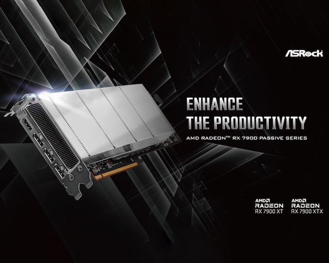

As sales of GPU-based AI accelerators remain as strong as ever, the immense demand for these cards has led to some server builders going off the beaten path in order to get the hardware they want at a lower price. While both NVIDIA and AMD offer official card configurations for servers, the correspondingly high price of these cards makes them a significant financial outlay that some customers either can't afford, or don't want to pay.
Instead, these groups have been turning to buying up consumer graphics cards, which although they come with additional limitations, are also a fraction of the cost of a "proper" server card. And this week, ASRock has removed another one of those limitations for would-be AMD Radeon users, with the introduction of a set of compact, passively-cooled Radeon RX 7900 XTX and RX 7900 XT video cards that are designed to go in servers.
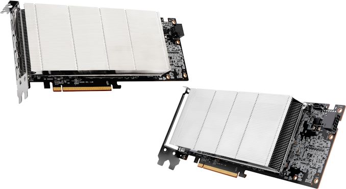
Without any doubts, ASRock's AMD Radeon RX 7900 XTX Passive 24GB and AMD Radeon RX 7900 XT Passive 20GB AIBs are indeed graphics cards with four display outputs and based on the Navi 31 graphics processor (with 6144 and 5376 stream processors, respectively), so they can output graphics and work both with games and professional applications. And with TGPs of 355W and 315W respectively, these cards aren't underclocked in any way compared to traditional desktop cards. However, unlike a typical desktop card, the cooler on these cards is a dual-slot heatsink without any kind of fan attached, which is meant to be used with high-airflow forced-air cooling.
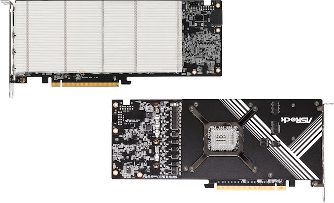
All-told, ASRock's passive cooler is pretty capable, as well; it's not just a simple aluminum heatsink. Beneath the fins, ASRock has gone with a vapor chamber and multiple heat pipes to distribute heat to the rest of the sink. Even with forced-air cooling in racked servers, the heatsink itself still needs to be efficient to keep a 300W+ card cool with only a dual-slot cooler – and especially so when upwards of four of these cards are installed side-by-side with each other. To make the boards even more server friendly, these cards are equipped with a 12V-2×6 power connector, a first for the Radeon RX 7900 series, simplifying installation by reducing cable clutter.
Driving the demand for these cards in particular is their memory configuration. With 24GB for the 7900 XTX and 20GB for the 7900 XT is half as much (or less) memory than can be found on AMD and NVIDIA's high-end professional and server cards, AMD is the only vendor offering consumer cards with this much memory for less than $1000. So for a memory-intensive AI inference cluster built on a low budget, the cheapest 24GB card available starts looking like a tantalizing option.
Otherwise, ASRock's Radeon RX 7900 Passive cards distinguish themselves from AMD's formal professional and server cards by what they're not capable of doing: namely, remote professional graphics or other applications that need things like GPU partitioning. These parts look to be aimed at one application only, artificial intelligence, and are meant to process huge amounts of data. For this purpose, their passive coolers will do the job and the lack of ProViz or VDI-oriented drives ensure that AMD will leave these lucrative markets for itself.
GPUs
Standard CPU coolers, while adequate for managing basic thermal loads, often fall short in terms of noise reduction and superior cooling efficiency. This limitation drives advanced users and system builders to seek aftermarket solutions tailored to their specific needs. The high-end aftermarket cooler market is highly competitive, with manufacturers striving to offer products with exceptional performance.
Endorfy, previously known as SilentiumPC, is a Polish manufacturer that has undergone a significant transformation to expand its presence in global markets. The brand is known for delivering high-performance cooling solutions with a strong focus on balancing efficiency and affordability. By rebranding as Endorfy, the company aims to enter premium market segments while continuing to offer reliable, high-quality cooling products.
SilentiumPC became very popular in the value/mainstream segments of the PC market with their products, the spearhead of which probably was the Fera 5 cooler that we reviewed a little over two years ago and had a remarkable value for money. Today’s review places Endorfy’s largest CPU cooler, the Fortis 5 Dual Fan, on our laboratory test bench. The Fortis 5 is the largest CPU air cooler the company currently offers and is significantly more expensive than the Fera 5, yet it still is a single-tower cooler that strives to strike a balance between value, compatibility, and performance.
Cases/Cooling/PSUs
Tenstorrent has unveiled its next-generation Wormhole processor for AI workloads that promises to offer decent performance at a low price. The company currently offers two add-on PCIe cards carrying one or two Wormhole processors as well as TT-LoudBox, and TT-QuietBox workstations aimed at software developers. The whole of today's release is aimed at developers rather than those who will deploy the Wormhole boards for their commercial workloads.
“It is always rewarding to get more of our products into developer hands. Releasing development systems with our Wormhole™ card helps developers scale up and work on multi-chip AI software.” said Jim Keller, CEO of Tenstorrent. “In addition to this launch, we are excited that the tape-out and power-on for our second generation, Blackhole, is going very well.”
Each Wormhole processor packs 72 Tensix cores (featuring five RISC-V cores supporting various data formats) with 108 MB of SRAM to deliver 262 FP8 TFLOPS at 1 GHz at 160W thermal design power. A single-chip Wormhole n150 card carries 12 GB of GDDR6 memory featuring a 288 GB/s bandwidth.
Wormhole processors offer flexible scalability to meet the varying needs of workloads. In a standard workstation setup with four Wormhole n300 cards, the processors can merge to function as a single unit, appearing as a unified, extensive network of Tensix cores to the software. This configuration allows the accelerators to either work on the same workload, be divided among four developers or run up to eight distinct AI models simultaneously. A crucial feature of this scalability is that it operates natively without the need for virtualization. In data center environments, Wormhole processors will scale both inside one machine using PCIe or outside of a single machine using Ethernet.
From performance standpoint, Tenstorrent's single-chip Wormhole n150 card (72 Tensix cores at 1 GHz, 108 MB SRAM, 12 GB GDDR6 at 288 GB/s) is capable of 262 FP8 TFLOPS at 160W, whereas the dual-chip Wormhole n300 board (128 Tensix cores at 1 GHz, 192 MB SRAM, aggregated 24 GB GDDR6 at 576 GB/s) can offer up to 466 FP8 TFLOPS at 300W (according to Tom's Hardware).
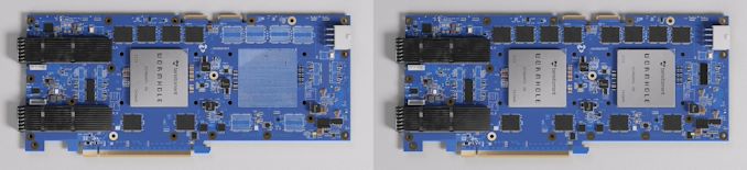
To put that 466 FP8 TFLOPS at 300W number into context, let's compare it to what AI market leader Nvidia has to offer at this thermal design power. Nvidia's A100 does not support FP8, but it does support INT8 and its peak performance is 624 TOPS (1,248 TOPS with sparsity). By contrast, Nvidia's H100 supports FP8 and its peak performance is massive 1,670 TFLOPS (3,341 TFLOPS with sparsity) at 300W, which is a big difference from Tenstorrent's Wormhole n300.
There is a big catch though. Tenstorrent's Wormhole n150 is offered for $999, whereas n300 is available for $1,399. By contrast, one Nvidia H100 card can retail for $30,000, depending on quantities. Of course, we do not know whether four or eight Wormhole processors can indeed deliver the performance of a single H300, though they will do so at 600W or 1200W TDP, respectively.
In addition to cards, Tenstorrent offers developers pre-built workstations with four n300 cards inside the less expensive Xeon-based TT-LoudBox with active cooling and a premium EPYC-powered TT-QuietBox with liquid cooling.
Sources: Tenstorrent, Tom's Hardware
AI
Standard CPU coolers, while adequate for managing basic thermal loads, often fall short in terms of noise reduction and superior cooling efficiency. This limitation drives advanced users and system builders to seek aftermarket solutions tailored to their specific needs. The high-end aftermarket cooler market is highly competitive, with manufacturers striving to offer products with exceptional performance.
Endorfy, previously known as SilentiumPC, is a Polish manufacturer that has undergone a significant transformation to expand its presence in global markets. The brand is known for delivering high-performance cooling solutions with a strong focus on balancing efficiency and affordability. By rebranding as Endorfy, the company aims to enter premium market segments while continuing to offer reliable, high-quality cooling products.
SilentiumPC became very popular in the value/mainstream segments of the PC market with their products, the spearhead of which probably was the Fera 5 cooler that we reviewed a little over two years ago and had a remarkable value for money. Today’s review places Endorfy’s largest CPU cooler, the Fortis 5 Dual Fan, on our laboratory test bench. The Fortis 5 is the largest CPU air cooler the company currently offers and is significantly more expensive than the Fera 5, yet it still is a single-tower cooler that strives to strike a balance between value, compatibility, and performance.
Cases/Cooling/PSUs
Tenstorrent has unveiled its next-generation Wormhole processor for AI workloads that promises to offer decent performance at a low price. The company currently offers two add-on PCIe cards carrying one or two Wormhole processors as well as TT-LoudBox, and TT-QuietBox workstations aimed at software developers. The whole of today's release is aimed at developers rather than those who will deploy the Wormhole boards for their commercial workloads.
“It is always rewarding to get more of our products into developer hands. Releasing development systems with our Wormhole™ card helps developers scale up and work on multi-chip AI software.” said Jim Keller, CEO of Tenstorrent. “In addition to this launch, we are excited that the tape-out and power-on for our second generation, Blackhole, is going very well.”
Each Wormhole processor packs 72 Tensix cores (featuring five RISC-V cores supporting various data formats) with 108 MB of SRAM to deliver 262 FP8 TFLOPS at 1 GHz at 160W thermal design power. A single-chip Wormhole n150 card carries 12 GB of GDDR6 memory featuring a 288 GB/s bandwidth.
Wormhole processors offer flexible scalability to meet the varying needs of workloads. In a standard workstation setup with four Wormhole n300 cards, the processors can merge to function as a single unit, appearing as a unified, extensive network of Tensix cores to the software. This configuration allows the accelerators to either work on the same workload, be divided among four developers or run up to eight distinct AI models simultaneously. A crucial feature of this scalability is that it operates natively without the need for virtualization. In data center environments, Wormhole processors will scale both inside one machine using PCIe or outside of a single machine using Ethernet.
From performance standpoint, Tenstorrent's single-chip Wormhole n150 card (72 Tensix cores at 1 GHz, 108 MB SRAM, 12 GB GDDR6 at 288 GB/s) is capable of 262 FP8 TFLOPS at 160W, whereas the dual-chip Wormhole n300 board (128 Tensix cores at 1 GHz, 192 MB SRAM, aggregated 24 GB GDDR6 at 576 GB/s) can offer up to 466 FP8 TFLOPS at 300W (according to Tom's Hardware).
To put that 466 FP8 TFLOPS at 300W number into context, let's compare it to what AI market leader Nvidia has to offer at this thermal design power. Nvidia's A100 does not support FP8, but it does support INT8 and its peak performance is 624 TOPS (1,248 TOPS with sparsity). By contrast, Nvidia's H100 supports FP8 and its peak performance is massive 1,670 TFLOPS (3,341 TFLOPS with sparsity) at 300W, which is a big difference from Tenstorrent's Wormhole n300.
There is a big catch though. Tenstorrent's Wormhole n150 is offered for $999, whereas n300 is available for $1,399. By contrast, one Nvidia H100 card can retail for $30,000, depending on quantities. Of course, we do not know whether four or eight Wormhole processors can indeed deliver the performance of a single H300, though they will do so at 600W or 1200W TDP, respectively.
In addition to cards, Tenstorrent offers developers pre-built workstations with four n300 cards inside the less expensive Xeon-based TT-LoudBox with active cooling and a premium EPYC-powered TT-QuietBox with liquid cooling.
Sources: Tenstorrent, Tom's Hardware
AI

Under the CHIPS & Science Act, the U.S. government provided tens of billions of dollars in grants and loans to the world's leading maker of chips, such as Intel, Samsung, and TSMC, which will significantly expand the country's semiconductor production industry in the coming years. However, most chips are typically tested, assembled, and packaged in Asia, which has left the American supply chain incomplete. Addressing this last gap in the government's domestic chip production plans, these past couple of weeks the U.S. government signed memorandums of understanding worth about $1.5 billion with Amkor and SK hynix to support their efforts to build chip packaging facilities in the U.S.
Amkor plans to build a $2 billion advanced packaging facility near Peoria, Arizona, to test and assemble chips produced by TSMC at its Fab 21 near Phoenix, Arizona. The company signed a MOU that offers $400 million in direct funding and access to $200 million in loans under the CHIPS & Science Act. In addition, the company plans to take advantage of a 25% investment tax credit on eligible capital expenditures.
Set to be strategically positioned near TSMC's upcoming Fab 21 complex in Arizona, Amkor's Peoria facility will occupy 55 acres and, when fully completed, will feature over 500,000 square feet (46,451 square meters) of cleanroom space, more than twice the size of Amkor's advanced packaging site in Vietnam. Although the company has not disclosed the exact capacity or the specific technologies the facility will support, it is expected to cater to a wide range of industries, including automotive, high-performance computing, and mobile technologies. This suggests the new plant will offer diverse packaging solutions, including traditional, 2.5D, and 3D technologies.
Amkor has collaborated extensively with Apple on the vision and initial setup of the Peoria facility, as Apple is slated to be the facility's first and largest customer, marking a significant commitment from the tech giant. This partnership highlights the importance of the new facility in reinforcing the U.S. semiconductor supply chain and positioning Amkor as a key partner for companies relying on TSMC's manufacturing capabilities. The project is expected to generate around 2,000 jobs and is scheduled to begin operations in 2027.
This week SK hynix also signed a preliminary agreement with the U.S. government to receive up to $450 million in direct funding and $500 million in loans to build an advanced memory packaging facility in West Lafayette, Indiana.
The proposed facility is scheduled to begin operations in 2028, which means that it will assemble HBM4 or HBM4E memory. Meanwhile, DRAM devices for high bandwidth memory (HBM) stacks will still be produced in South Korea. Nonetheless, packing finished HBM4/HBM4E in the U.S. and possibly integrating these memory modules with high-end processors is a big deal.
In addition to building its packaging plant, SK hynix plans to collaborate with Purdue University and other local research institutions to advance semiconductor technology and packaging innovations. This partnership is intended to bolster research and development in the region, positioning the facility as a hub for AI technology and skilled employment.
Semiconductors

Kioxia's booth at FMS 2024 was a busy one with multiple technology demonstrations keeping visitors occupied. A walk-through of the BiCS 8 manufacturing process was the first to grab my attention. Kioxia and Western Digital announced the sampling of BiCS 8 in March 2023. We had touched briefly upon its CMOS Bonded Array (CBA) scheme in our coverage of Kioxial's 2Tb QLC NAND device and coverage of Western Digital's 128 TB QLC enterprise SSD proof-of-concept demonstration. At Kioxia's booth, we got more insights.

Traditionally, fabrication of flash chips involved placement of the associate logic circuitry (CMOS process) around the periphery of the flash array. The process then moved on to putting the CMOS under the cell array, but the wafer development process was serialized with the CMOS logic getting fabricated first followed by the cell array on top. However, this has some challenges because the cell array requires a high-temperature processing step to ensure higher reliability that can be detrimental to the health of the CMOS logic. Thanks to recent advancements in wafer bonding techniques, the new CBA process allows the CMOS wafer and cell array wafer to be processed independently in parallel and then pieced together, as shown in the models above.

The BiCS 8 3D NAND incorporates 218 layers, compared to 112 layers in BiCS 5 and 162 layers in BiCS 6. The company decided to skip over BiCS 7 (or, rather, it was probably a short-lived generation meant as an internal test vehicle). The generation retains the four-plane charge trap structure of BiCS 6. In its TLC avatar, it is available as a 1 Tbit device. The QLC version is available in two capacities - 1 Tbit and 2 Tbit.
Kioxia also noted that while the number of layers (218) doesn't compare favorably with the latest layer counts from the competition, its lateral scaling / cell shrinkage has enabled it to be competitive in terms of bit density as well as operating speeds (3200 MT/s). For reference, the latest shipping NAND from Micron - the G9 - has 276 layers with a bit density in TLC mode of 21 Gbit/mm2, and operates at up to 3600 MT/s. However, its 232L NAND operates only up to 2400 MT/s and has a bit density of 14.6 Gbit/mm2.
It must be noted that the CBA hybrid bonding process has advantages over the current processes used by other vendors - including Micron's CMOS under array (CuA) and SK hynix's 4D PUC (periphery-under-chip) developed in the late 2010s. It is expected that other NAND vendors will also move eventually to some variant of the hybrid bonding scheme used by Kioxia.
Storage
Lorem Ipsum is simply dummy text of the printing and typesetting industry. Lorem Ipsum has been the industry's.
Standard CPU coolers, while adequate for managing basic thermal loads, often fall short in terms of noise reduction and superior cooling efficiency. This limitation drives advanced users and system builders to seek aftermarket solutions tailored to their specific needs. The high-end aftermarket cooler market is highly competitive, with manufacturers striving to offer products with exceptional performance.
Endorfy, previously known as SilentiumPC, is a Polish manufacturer that has undergone a significant transformation to expand its presence in global markets. The brand is known for delivering high-performance cooling solutions with a strong focus on balancing efficiency and affordability. By rebranding as Endorfy, the company aims to enter premium market segments while continuing to offer reliable, high-quality cooling products.
SilentiumPC became very popular in the value/mainstream segments of the PC market with their products, the spearhead of which probably was the Fera 5 cooler that we reviewed a little over two years ago and had a remarkable value for money. Today’s review places Endorfy’s largest CPU cooler, the Fortis 5 Dual Fan, on our laboratory test bench. The Fortis 5 is the largest CPU air cooler the company currently offers and is significantly more expensive than the Fera 5, yet it still is a single-tower cooler that strives to strike a balance between value, compatibility, and performance.
Cases/Cooling/PSUs

, so they can output graphics and work both with games and professional applications. And with TGPs of 355W and 315W respectively, these cards aren't underclocked in any way compared to traditional desktop cards. However, unlike a typical desktop card, the cooler on these cards is a dual-slot heatsink without any kind of fan attached, which is meant to be used with high-airflow forced-air cooling.</p>
<p style="text-align: center;"><a href="https://www.anandtech.com/show/21491/asrock-launches-passively-cooled-radeon-rx-7900-xtx-and-xt"><img alt="" src="https://images.anandtech.com/doci/21491/ASRock-Launches-AMD-Radeon--RX-790-0-Passive-1_575px.jpg" /></a></p>
<p>All-told, ASRock's passive cooler is pretty capable, as well; it's not just a simple aluminum heatsink. Beneath the fins, ASRock has gone with a vapor chamber and multiple heat pipes to distribute heat to the rest of the sink. Even with forced-air cooling in racked servers, the heatsink itself still needs to be efficient to keep a 300W+ card cool with only a dual-slot cooler – and especially so when upwards of four of these cards are installed side-by-side with each other. To make the boards even more server friendly, these cards are equipped with a 12V-2×6 power connector, a first for the Radeon RX 7900 series, simplifying installation by reducing cable clutter.</p>
<p style="text-align: center;"><a href="https://www.anandtech.com/show/21491/asrock-launches-passively-cooled-radeon-rx-7900-xtx-and-xt"><img alt="" src="https://images.anandtech.com/doci/21491/ASRock-Launches-AMD-Radeon--RX-790-0-Passive-2_575px.jpg" /></a></p>
<p>Driving the demand for these cards in particular is their memory configuration. With 24GB for the 7900 XTX and 20GB for the 7900 XT is half as much (or less) memory than can be found on AMD and NVIDIA's high-end professional and server cards, AMD is the only vendor offering consumer cards with this much memory for less than $1000. So for a memory-intensive AI inference cluster built on a low budget, the cheapest 24GB card available starts looking like a tantalizing option.</p>
<p>Otherwise, ASRock's Radeon RX 7900 Passive cards distinguish themselves from AMD's formal professional and server cards by what they're <em>not</em> capable of doing: namely, remote professional graphics or other applications that need things like GPU partitioning. These parts look to be aimed at one application only, artificial intelligence, and are meant to process huge amounts of data. For this purpose, their passive coolers will do the job and the lack of ProViz or VDI-oriented drives ensure that AMD will leave these lucrative markets for itself.</p>
</p> GPUs)
, so they can output graphics and work both with games and professional applications. And with TGPs of 355W and 315W respectively, these cards aren't underclocked in any way compared to traditional desktop cards. However, unlike a typical desktop card, the cooler on these cards is a dual-slot heatsink without any kind of fan attached, which is meant to be used with high-airflow forced-air cooling.</p>
<p style="text-align: center;"><a href="https://www.anandtech.com/show/21491/asrock-launches-passively-cooled-radeon-rx-7900-xtx-and-xt"><img alt="" src="https://images.anandtech.com/doci/21491/ASRock-Launches-AMD-Radeon--RX-790-0-Passive-1_575px.jpg" /></a></p>
<p>All-told, ASRock's passive cooler is pretty capable, as well; it's not just a simple aluminum heatsink. Beneath the fins, ASRock has gone with a vapor chamber and multiple heat pipes to distribute heat to the rest of the sink. Even with forced-air cooling in racked servers, the heatsink itself still needs to be efficient to keep a 300W+ card cool with only a dual-slot cooler – and especially so when upwards of four of these cards are installed side-by-side with each other. To make the boards even more server friendly, these cards are equipped with a 12V-2×6 power connector, a first for the Radeon RX 7900 series, simplifying installation by reducing cable clutter.</p>
<p style="text-align: center;"><a href="https://www.anandtech.com/show/21491/asrock-launches-passively-cooled-radeon-rx-7900-xtx-and-xt"><img alt="" src="https://images.anandtech.com/doci/21491/ASRock-Launches-AMD-Radeon--RX-790-0-Passive-2_575px.jpg" /></a></p>
<p>Driving the demand for these cards in particular is their memory configuration. With 24GB for the 7900 XTX and 20GB for the 7900 XT is half as much (or less) memory than can be found on AMD and NVIDIA's high-end professional and server cards, AMD is the only vendor offering consumer cards with this much memory for less than $1000. So for a memory-intensive AI inference cluster built on a low budget, the cheapest 24GB card available starts looking like a tantalizing option.</p>
<p>Otherwise, ASRock's Radeon RX 7900 Passive cards distinguish themselves from AMD's formal professional and server cards by what they're <em>not</em> capable of doing: namely, remote professional graphics or other applications that need things like GPU partitioning. These parts look to be aimed at one application only, artificial intelligence, and are meant to process huge amounts of data. For this purpose, their passive coolers will do the job and the lack of ProViz or VDI-oriented drives ensure that AMD will leave these lucrative markets for itself.</p>
</p> GPUs | https://compbuddey.blogspot.com/2024/08/asrock-launches-passively-cooled-radeon_2.html)
, so they can output graphics and work both with games and professional applications. And with TGPs of 355W and 315W respectively, these cards aren't underclocked in any way compared to traditional desktop cards. However, unlike a typical desktop card, the cooler on these cards is a dual-slot heatsink without any kind of fan attached, which is meant to be used with high-airflow forced-air cooling.</p>
<p style="text-align: center;"><a href="https://www.anandtech.com/show/21491/asrock-launches-passively-cooled-radeon-rx-7900-xtx-and-xt"><img alt="" src="https://images.anandtech.com/doci/21491/ASRock-Launches-AMD-Radeon--RX-790-0-Passive-1_575px.jpg" /></a></p>
<p>All-told, ASRock's passive cooler is pretty capable, as well; it's not just a simple aluminum heatsink. Beneath the fins, ASRock has gone with a vapor chamber and multiple heat pipes to distribute heat to the rest of the sink. Even with forced-air cooling in racked servers, the heatsink itself still needs to be efficient to keep a 300W+ card cool with only a dual-slot cooler – and especially so when upwards of four of these cards are installed side-by-side with each other. To make the boards even more server friendly, these cards are equipped with a 12V-2×6 power connector, a first for the Radeon RX 7900 series, simplifying installation by reducing cable clutter.</p>
<p style="text-align: center;"><a href="https://www.anandtech.com/show/21491/asrock-launches-passively-cooled-radeon-rx-7900-xtx-and-xt"><img alt="" src="https://images.anandtech.com/doci/21491/ASRock-Launches-AMD-Radeon--RX-790-0-Passive-2_575px.jpg" /></a></p>
<p>Driving the demand for these cards in particular is their memory configuration. With 24GB for the 7900 XTX and 20GB for the 7900 XT is half as much (or less) memory than can be found on AMD and NVIDIA's high-end professional and server cards, AMD is the only vendor offering consumer cards with this much memory for less than $1000. So for a memory-intensive AI inference cluster built on a low budget, the cheapest 24GB card available starts looking like a tantalizing option.</p>
<p>Otherwise, ASRock's Radeon RX 7900 Passive cards distinguish themselves from AMD's formal professional and server cards by what they're <em>not</em> capable of doing: namely, remote professional graphics or other applications that need things like GPU partitioning. These parts look to be aimed at one application only, artificial intelligence, and are meant to process huge amounts of data. For this purpose, their passive coolers will do the job and the lack of ProViz or VDI-oriented drives ensure that AMD will leave these lucrative markets for itself.</p>
</p> GPUs&body=https://compbuddey.blogspot.com/2024/08/asrock-launches-passively-cooled-radeon_2.html)
0 Comments