Hot Posts
End of the Road: An AnandTech Farewell
It is with great sadness that I find myself penning the hardest news post I’ve ever needed to write here at AnandTech. After over 27 years of covering the wide – and wild – world of computing hardware, today is AnandTech’s final day of publication.
For better or worse, we’ve reached the end of a long journey – one that started with a review of an AMD processor, and has ended with the review of an AMD processor. It’s fittingly poetic, but it is also a testament to the fact that we’ve spent the last 27 years doing what we love, covering the chips that are the lifeblood of the computing industry.
A lot of things have changed in the last quarter-century – in 1997 NVIDIA had yet to even coin the term “GPU” – and we’ve been fortunate to watch the world of hardware continue to evolve over the time period. We’ve gone from boxy desktop computers and laptops that today we’d charitably classify as portable desktops, to pocket computers where even the cheapest budget device puts the fastest PC of 1997 to shame.
The years have also brought some monumental changes to the world of publishing. AnandTech was hardly the first hardware enthusiast website, nor will we be the last. But we were fortunate to thrive in the past couple of decades, when so many of our peers did not, thanks to a combination of hard work, strategic investments in people and products, even more hard work, and the support of our many friends, colleagues, and readers.
Still, few things last forever, and the market for written tech journalism is not what it once was – nor will it ever be again. So, the time has come for AnandTech to wrap up its work, and let the next generation of tech journalists take their place within the zeitgeist.
It has been my immense privilege to write for AnandTech for the past 19 years – and to manage it as its editor-in-chief for the past decade. And while I carry more than a bit of remorse in being AnandTech’s final boss, I can at least take pride in everything we’ve accomplished over the years, whether it’s lauding some legendary products, writing technology primers that still remain relevant today, or watching new stars rise in expected places. There is still more that I had wanted AnandTech to do, but after 21,500 articles, this was a good start.
And while the AnandTech staff is riding off into the sunset, I am happy to report that the site itself won’t be going anywhere for a while. Our publisher, Future PLC, will be keeping the AnandTech website and its many articles live indefinitely. So that all of the content we’ve created over the years remains accessible and citable. Even without new articles to add to the collection, I expect that many of the things we’ve written over the past couple of decades will remain relevant for years to come – and remain accessible just as long.
The AnandTech Forums will also continue to be operated by Future’s community team and our dedicated troop of moderators. With forum threads going back to 1999 (and some active members just as long), the forums have a history almost as long and as storied as AnandTech itself (wounded monitor children, anyone?). So even when AnandTech is no longer publishing articles, we’ll still have a place for everyone to talk about the latest in technology – and have those discussions last longer than 48 hours.
Finally, for everyone who still needs their technical writing fix, our formidable opposition of the last 27 years and fellow Future brand, Tom’s Hardware, is continuing to cover the world of technology. There are a couple of familiar AnandTech faces already over there providing their accumulated expertise, and the site will continue doing its best to provide a written take on technology news.
So Many Thank Yous
As I look back on everything AnandTech has accomplished over the past 27 years, there are more than a few people, groups, and companies that I would like to thank on behalf of both myself and AnandTech as a whole.
First and foremost, I cannot thank enough all the editors who have worked for AnandTech over the years. T... Site Updates
-
Newer
Western Digital Introduces 4 TB microSDUC, 8 TB SDUC, and 16 TB External SSDs Western Digital's BiCS8 218-layer 3D NAND is being put to good use in a wide range of client and enterprise platforms, including WD's upcoming Gen 5 client SSDs and 128 TB-class datacenter SSD. On the external storage front, the company demonstrated four different products: for card-based media, 4 TB microSDUC and 8 TB SDUC cards with UHS-I speeds, and on the portable SSD front we had two 16 TB drives. One will be a SanDisk Desk Drive with external power, and the other in the SanDisk Extreme Pro housing with a lanyard opening in the case. All of these are using BiCS8 QLC NAND, though I did hear booth talk (as I was taking leave) that they were not supposed to divulge the use of QLC in these products. The 4 TB microSDUC and 8 TB SDUC cards are rated for UHS-I speeds. They are being marketed under the SanDisk Ultra branding. The SanDisk Desk Drive is an external SSD with a 18W power adapter, and it has been in the market for a few months now. Initially launched in capacities up to 8 TB, Western Digital had promised a 16 TB version before the end of the year. It appears that the product is coming to retail quite soon. One aspect to note is that this drive has been using TLC for the SKUs that are currently in the market, so it appears unlikely that the 16 TB version would be QLC. The units (at least up to the 8 TB capacity point) come with two SN850XE drives. Given the recent introduction of the 8 TB SN850X, an 'E' version with tweaked firmware is likely to be present in the 16 TB Desk Drive. The 16 TB portable SSD in the SanDisk Extreme housing was a technology demonstration. It is definitely the highest capacity bus-powered portable SSD demonstrated by any vendor at any trade show thus far. Given the 16 TB Desk Drive's imminent market introduction, it is just a matter of time before the technology demonstration of the bus-powered version becomes a retail reality. Storage
-
Older
Western Digital Introduces 4 TB microSDUC, 8 TB SDUC, and 16 TB External SSDs Western Digital's BiCS8 218-layer 3D NAND is being put to good use in a wide range of client and enterprise platforms, including WD's upcoming Gen 5 client SSDs and 128 TB-class datacenter SSD. On the external storage front, the company demonstrated four different products: for card-based media, 4 TB microSDUC and 8 TB SDUC cards with UHS-I speeds, and on the portable SSD front we had two 16 TB drives. One will be a SanDisk Desk Drive with external power, and the other in the SanDisk Extreme Pro housing with a lanyard opening in the case. All of these are using BiCS8 QLC NAND, though I did hear booth talk (as I was taking leave) that they were not supposed to divulge the use of QLC in these products. The 4 TB microSDUC and 8 TB SDUC cards are rated for UHS-I speeds. They are being marketed under the SanDisk Ultra branding. The SanDisk Desk Drive is an external SSD with a 18W power adapter, and it has been in the market for a few months now. Initially launched in capacities up to 8 TB, Western Digital had promised a 16 TB version before the end of the year. It appears that the product is coming to retail quite soon. One aspect to note is that this drive has been using TLC for the SKUs that are currently in the market, so it appears unlikely that the 16 TB version would be QLC. The units (at least up to the 8 TB capacity point) come with two SN850XE drives. Given the recent introduction of the 8 TB SN850X, an 'E' version with tweaked firmware is likely to be present in the 16 TB Desk Drive. The 16 TB portable SSD in the SanDisk Extreme housing was a technology demonstration. It is definitely the highest capacity bus-powered portable SSD demonstrated by any vendor at any trade show thus far. Given the 16 TB Desk Drive's imminent market introduction, it is just a matter of time before the technology demonstration of the bus-powered version becomes a retail reality. Storage
You may like these posts
The Corsair iCUE LINK TITAN 360 RX RGB AIO Cooler Review: Meticulous, But Pricey Corsair, a longstanding and esteemed manufacturer in the PC components industry, initially built its reputation on memory-related products. However, nearly two decades ago, Corsair began diversifying its product line. This expansion started cautiously, with a limited number of products, but quickly proved to be highly successful, propelling Corsair into the industry powerhouse it is today. One of Corsair's most triumphant product categories is all-in-one (AIO) liquid coolers. This success is particularly notable given that their initial foray into liquid cooling in 2003 did not meet expectations. However, Corsair didn’t throw in the towel. Undeterred, they re-entered the market years later, leveraging the growing popularity of user-friendly, maintenance-free AIO designs. This gamble paid off handsomely, as AIO coolers are now one of Corsair’s flagship product lines, boasting a wide array of models. In this review, we focus on the latest addition to Corsair's AIO cooler lineup: the iCUE LINK TITAN 360 RX. This model is similar to the iCUE LINK H150i RGB, but introduces subtle yet significant improvements, including a performance upgrade with an enhanced pump. The TITAN 360 RX continues Corsair's tradition of innovation and quality, seamlessly integrating into the iCUE ecosystem for an optimized user experience. Its single-cable design ensures a clean and effortless installation, making it a standout in Corsair's evolving cooler lineup. Cases/Cooling/PSUs
July 30, 2025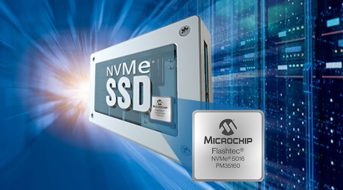
Microchip Demonstrates Flashtec 5016 Enterprise SSD Controller Microchip recently announced the availability of their second PCIe Gen 5 enterprise SSD controller - the Flashtec 5016. Like the 4016, this is also a 16-channel controller, but there are some key updates: PCIe 5.0 lane organization: Operation in x4 or dual independent x2 / x2 mode in the 5016, compared to the x8, or x4, or dual independent x4 / x2 mode in the 4016. DRAM support: Four ranks of DDR5-5200 in the 5016, compared to two ranks of DDR4-3200 in the 4016. Extended NAND support: 2400 MT/s NAND in the 4016, compared to the 3200 MT/s NAND support in the 5016. Performance improvements: The 5016 is capable of delivering 3.5M+ random read IOPS compared to the 3M+ of the 4016. Microchip's enterprise SSD controllers provide a high level of flexibility to SSD vendors by providing them with significant horsepower and accelerators. The 5016 includes Cortex-A53 cores for SSD vendors to run custom applications relevant to SSD management. However, compared to the Gen4 controllers, there are two additional cores in the CPU cluster. The DRAM subsystem includes ECC support (both out-of-band and inline, as desired by the SSD vendor). At FMS 2024, the company demonstrated an application of the neural network engines embedded in the Gen5 controllers. Controllers usually employ a 'read-retry' operation with altered read-out voltages for flash reads that do not complete successfully. Microchip implemented a machine learning approach to determine the read-out voltage based on the health history of the NAND block using the NN engines in the controller. This approach delivers tangible benefits for read latency and power consumption (thanks to a smaller number of errors on the first read). The 4016 and 5016 come with a single-chip root of trust implementation for hardware security. A secure boot process with dual-signature authentication ensures that the controller firmware is not maliciously altered in the field. The company also brought out the advantages of their controller's implementation of SR-IOV, flexible data placement, and zoned namespaces along with their 'credit engine' scheme for multi-tenant cloud workloads. These aspects were also brought out in other demonstrations. Microchip's press release included quotes from the usual NAND vendors - Solidigm, Kioxia, and Micron. On the customer front, Longsys has been using Flashtec controllers in their enterprise offerings along with YMTC NAND. It is likely that this collaboration will continue further using the new 5016 controller. Storage
July 29, 2025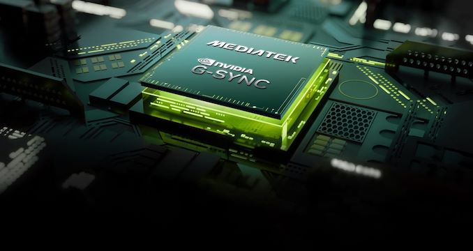
MediaTek to Add NVIDIA G-Sync Support to Monitor Scalers, Make G-Sync Displays More Accessible NVIDIA on Tuesday said that future monitor scalers from MediaTek will support its G-Sync technologies. NVIDIA is partnering with MediaTek to integrate its full range of G-Sync technologies into future monitors without requiring a standalone G-Sync module, which makes advanced gaming features more accessible across a broader range of displays. Traditionally, G-Sync technology relied on a dedicated G-sync module – based on an Altera FPGA – to handle syncing display refresh rates with the GPU in order to reduce screen tearing, stutter, and input lag. As a more basic solution, in 2019 NVIDIA introduced G-Sync Compatible certification and branding, which leveraged the industry-standard VESA AdaptiveSync technology to handle variable refresh rates. In lieu of using a dedicated module, leveraging AdaptiveSync allowed for cheaper monitors, with NVIDIA's program serving as a stamp of approval that the monitor worked with NVIDIA GPUs and met NVIDIA's performance requirements. Still, G-Sync Compatible monitors still lack some features that, to date, require the dedicated G-Sync module. Through this new partnership with MediaTek, MediaTek will bring support for all of NVIDIA's G-Sync technologies, including the latest G-Sync Pulsar, directly into their scalers. G-Sync Pulsar enhances motion clarity and reduces ghosting, providing a smoother gaming experience. In addition to variable refresh rates and Pulsar, MediaTek-based G-Sync displays will support such features as variable overdrive, 12-bit color, Ultra Low Motion Blur, low latency HDR, and Reflex Analyzer. This integration will allow more monitors to support a full range of G-Sync features without having to incorporate an expensive FPGA. The first monitors to feature full G-Sync support without needing an NVIDIA module include the AOC Agon Pro AG276QSG2, Acer Predator XB273U F5, and ASUS ROG Swift 360Hz PG27AQNR. These monitors offer 360Hz refresh rates, 1440p resolution, and HDR support. What remains to be seen is which specific MediaTek's scalers will support NVIDIA's G-Sync technology – or if the company is going to implement support into all of their scalers going forward. It also remains to be seen whether monitors with NVIDIA's dedicated G-Sync modules retain any advantages over displays with MediaTek's scalers. Monitors
July 29, 2025
Popular Post
Kioxia Details BiCS 8 NAND at FMS 2024: 218 Layers With Superior Scaling
Kioxia's booth at FMS 2024 was a busy one with multiple technology demonstrations keeping visitors occupied. A walk-through of the BiCS 8 manufacturing process was the first to grab my attention. Kioxia and Western Digital announced the sampling of BiCS 8 in March 2023. We had touched briefly upon its CMOS Bonded Array (CBA) scheme in our coverage of Kioxial's 2Tb QLC NAND device and coverage of Western Digital's 128 TB QLC enterprise SSD proof-of-concept demonstration. At Kioxia's booth, we got more insights.
Traditionally, fabrication of flash chips involved placement of the associate logic circuitry (CMOS process) around the periphery of the flash array. The process then moved on to putting the CMOS under the cell array, but the wafer development process was serialized with the CMOS logic getting fabricated first followed by the cell array on top. However, this has some challenges because the cell array requires a high-temperature processing step to ensure higher reliability that can be detrimental to the health of the CMOS logic. Thanks to recent advancements in wafer bonding techniques, the new CBA process allows the CMOS wafer and cell array wafer to be processed independently in parallel and then pieced together, as shown in the models above.
The BiCS 8 3D NAND incorporates 218 layers, compared to 112 layers in BiCS 5 and 162 layers in BiCS 6. The company decided to skip over BiCS 7 (or, rather, it was probably a short-lived generation meant as an internal test vehicle). The generation retains the four-plane charge trap structure of BiCS 6. In its TLC avatar, it is available as a 1 Tbit device. The QLC version is available in two capacities - 1 Tbit and 2 Tbit.
Kioxia also noted that while the number of layers (218) doesn't compare favorably with the latest layer counts from the competition, its lateral scaling / cell shrinkage has enabled it to be competitive in terms of bit density as well as operating speeds (3200 MT/s). For reference, the latest shipping NAND from Micron - the G9 - has 276 layers with a bit density in TLC mode of 21 Gbit/mm2, and operates at up to 3600 MT/s. However, its 232L NAND operates only up to 2400 MT/s and has a bit density of 14.6 Gbit/mm2.
It must be noted that the CBA hybrid bonding process has advantages over the current processes used by other vendors - including Micron's CMOS under array (CuA) and SK hynix's 4D PUC (periphery-under-chip) developed in the late 2010s. It is expected that other NAND vendors will also move eventually to some variant of the hybrid bonding scheme used by Kioxia.
StorageFadu's FC5161 SSD Controller Breaks Cover in Western Digital's PCIe Gen5 Enterprise Drives
When Western Digital introduced its Ultrastar DC SN861 SSDs earlier this year, the company did not disclose which controller it used for these drives, which made many observers presume that WD was using an in-house controller. But a recent teardown of the drive shows that is not the case; instead, the company is using a controller from Fadu, a South Korean company founded in 2015 that specializes on enterprise-grade turnkey SSD solutions.
The Western Digital Ultrastar DC SN861 SSD is aimed at performance-hungry hyperscale datacenters and enterprise customers which are adopting PCIe Gen5 storage devices these days. And, as uncovered in photos from a recent Storage Review article, the drive is based on Fadu's FC5161 NVMe 2.0-compliant controller. The FC5161 utilizes 16 NAND channels supporting an ONFi 5.0 2400 MT/s interface, and features a combination of enterprise-grade capabilities (OCP Cloud Spec 2.0, SR-IOV, up to 512 name spaces for ZNS support, flexible data placement, NVMe-MI 1.2, advanced security, telemetry, power loss protection) not available on other off-the-shelf controllers – or on any previous Western Digital controllers.
The Ultrastar DC SN861 SSD offers sequential read speeds up to 13.7 GB/s as well as sequential write speeds up to 7.5 GB/s. As for random performance, it boasts with an up to 3.3 million random 4K read IOPS and up to 0.8 million random 4K write IOPS. The drives are available in capacities between 1.6 TB and 7.68 TB with one or three drive writes per day (DWPD) over five years rating as well as in U.2 and E1.S form-factors.
While the two form factors of the SN861 share a similar technical design, Western Digital has tailored each version for distinct workloads: the E1.S supports FDP and performance enhancements specifically for cloud environments. By contrast, the U.2 model is geared towards high-performance enterprise tasks and emerging applications like AI.
Without any doubts, Western Digital's Ultrastar DC SN861 is a feature-rich high-performance enterprise-grade SSD. It has another distinctive feature: a 5W idle power consumption, which is rather low by the standards of enterprise-grade drives (e.g., it is 1W lower compared to the SN840). While the difference with predecessors may be just 1W, hyperscalers deploy thousands of drives and for their TCO every watt counts.
Western Digital's Ultrastar DC SN861 SSDs are now available for purchase to select customers (such as Meta) and to interested parties. Prices are unknown, but they will depend on such factors as volumes.
Sources: Fadu, Storage Review
StorageIntel and Sandia National Labs Roll Out 1.15B Neuron “Hala Point” Neuromorphic Research System
While neuromorphic computing remains under research for the time being, efforts into the field have continued to grow over the years, as have the capabilities of the specialty chips that have been developed for this research. Following those lines, this morning Intel and Sandia National Laboratories are celebrating the deployment of the Hala Point neuromorphic system, which the two believe is the highest capacity system in the world. With 1.15 billion neurons overall, Hala Point is the largest deployment yet for Intel’s Loihi 2 neuromorphic chip, which was first announced at the tail-end of 2021.
The Hala Point system incorporates 1152 Loihi 2 processors, each of which is capable of simulating a million neurons. As noted back at the time of Loihi 2’s launch, these chips are actually rather small – just 31 mm2 per chip with 2.3 billion transistors each, as they’re built on the Intel 4 process (one of the only other Intel chips to do so, besides Meteor Lake). As a result, the complete system is similarly petite, taking up just 6 rack units of space (or as Sandia likes to compare it to, about the size of a microwave), with a power consumption of 2.6 kW. Now that it’s online, Hala Point has dethroned the SpiNNaker system as the largest disclosed neuromorphic system, offering admittedly just a slightly larger number of neurons at less than 3% of the power consumption of the 100 kW British system.
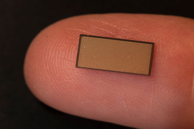
A Single Loihi 2 Chip (31 mm2)
Hala Point will be replacing an older Intel neuromorphic system at Sandia, Pohoiki Springs, which is based on Intel’s first-generation Loihi chips. By comparison, Hala Point offers ten-times as many neurons, and upwards of 12x the performance overall,
Both neuromorphic systems have been procured by Sandia in order to advance the national lab’s research into neuromorphic computing, a computing paradigm that behaves like a brain. The central thought (if you’ll excuse the pun) is that by mimicking the wetware writing this article, neuromorphic chips can be used to solve problems that conventional processors cannot solve today, and that they can do so more efficiently as well.
Sandia, for its part, has said that it will be using the system to look at large-scale neuromorphic computing, with work operating on a scale well beyond Pohoiki Springs. With Hala Point offering a simulated neuron count very roughly on the level of complexity of an owl brain, the lab believes that a larger-scale system will finally enable them to properly exploit the properties of neuromorphic computing to solve real problems in fields such as device physics, computer architecture, computer science and informatics, moving well beyond the simple demonstrations initially achieved at a smaller scale.
One new focus from the lab, which in turn has caught Intel’s attention, is the applicability of neuromorphic computing towards AI inference. Because the neural networks themselves behind the current wave of AI systems are attempting to emulate the human brain, in a sense, there is an obvious degree of synergy with the brain-mimicking neuromorphic chips, even if the algorithms differ in some key respects. Still, with energy efficiency being one of the major benefits of neuromorphic computing, it’s pushed Intel to look into the matter further – and even build a second, Hala Point-sized system of their own.
According to Intel, in their research on Hala Point, the system has reached efficiencies as high as 15 TOPS-per-Watt at 8-bit precision, albeit while using 10:1 sparsity, making it more than competitive with current-generation commercial chips. As an added bonus to that efficiency, the neuromorphic systems don’t require extensive data processing and batching in advance, which is normally necessary to make efficient use of the high density ALU arrays in GPUs and GPU-like processors.
Perhaps the most interesting use case of all, however, is the potent... CPUs
TSMC's 1.6nm Technology Announced for Late 2026: A16 with "Super Power Rail" Backside Power With the arrival of spring comes showers, flowers, and in the technology industry, TSMC's annual technology symposium series. With customers spread all around the world, the Taiwanese pure play foundry has adopted an interesting strategy for updating its customers on its fab plans, holding a series of symposiums from Silicon Valley to Shanghai. Kicking off the series every year – and giving us our first real look at TSMC's updated foundry plans for the coming years – is the Santa Clara stop, where yesterday the company has detailed several new technologies, ranging from more advanced lithography processes to massive, wafer-scale chip packing options.
Today we're publishing several stories based on TSMC's different offerings, starting with TSMC's marquee announcement: their A16 process node. Meanwhile, for the rest of our symposium stories, please be sure to check out the related reading below, and check back for additional stories.
- TSMC 2nm Update: N2 In 2025, N2P Loses Backside Power, and NanoFlex Brings Optimal Cells
- TSMC Preps Cheaper 4nm N4C Process For 2025, Aiming For 8.5% Cost Reduction
- TSMC's System-on-Wafer Platform Goes 3D: CoW-SoW Stacks Up the Chips
- TSMC Jumps Into Silicon Photonics, Lays Out Roadmap For 12.8 Tbps COUPE On-Package Interconnect
Headlining its Silicon Valley stop, TSMC announced its first 'angstrom-class' process technology: A16. Following a production schedule shift that has seen backside power delivery network technology (BSPDN) removed from TSMC's N2P node, the new 1.6nm-class production node will now be the first process to introduce BSPDN to TSMC's chipmaking repertoire. With the addition of backside power capabilities and other improvements, TSMC expects A16 to offer significantly improved performance and energy efficiency compared to TSMC's N2P fabrication process. It will be available to TSMC's clients starting H2 2026.
TSMC A16: Combining GAAFET With Backside Power Delivery
At a high level, TSMC's A16 process technology will rely on gate-all-around (GAAFET) nanosheet transistors and will feature a backside power rail, which will both improve power delivery and moderately increase transistor density. Compared to TSMC's N2P fabrication process, A16 is expected to offer a performance improvement of 8% to 10% at the same voltage and complexity, or a 15% to 20% reduction in power consumption at the same frequency and transistor count. TSMC is not listing detailed density parameters this far out, but the company says that chip density will increase by 1.07x to 1.10x – keeping in mind that transistor density heavily depends on the type and libraries of transistors used.
The key innovation of TSMC's A16 node, is its Super Power Rail (SPR) backside power delivery network, a first for TSMC. The contract chipmaker claims that A16's SPR is specifically tailored for high-performance computing products that feature both complex signal routes and dense power circuitry.
As noted earlier, with this week's announcement, A16 has now become the launch vehicle for backside power delivery at TSMC. The company was initially slated to offer BSPDN technology with N2P in 2026, but for reasons that aren't entirely clear, the tech has been punted from N2P and moved to A16. TSMC's official timing for N2P in 2023 was always a bit loose, so it's hard to say if this represents much of a practical delay for BSPDN at TSMC. But at the same time, it's important to underscore that A16 isn't just N2P renamed, but rather it will be a distinct technology from N2P.
TSMC is not the only fab pursuing backside power delivery, and accordingly, we're seeing multiple variations on the technique crop up at different fabs. The... Semiconductors
Search This Blog
OfferNest
Subscribe Us
Most Popular
Kioxia Details BiCS 8 NAND at FMS 2024: 218 Layers With Superior Scaling
Kioxia's booth at FMS 2024 was a busy one with multiple technology demonstrations keeping visitors occupied. A walk-through of the BiCS 8 manufacturing process was the first to grab my attention. Kioxia and Western Digital announced the sampling of BiCS 8 in March 2023. We had touched briefly upon its CMOS Bonded Array (CBA) scheme in our coverage of Kioxial's 2Tb QLC NAND device and coverage of Western Digital's 128 TB QLC enterprise SSD proof-of-concept demonstration. At Kioxia's booth, we got more insights.
Traditionally, fabrication of flash chips involved placement of the associate logic circuitry (CMOS process) around the periphery of the flash array. The process then moved on to putting the CMOS under the cell array, but the wafer development process was serialized with the CMOS logic getting fabricated first followed by the cell array on top. However, this has some challenges because the cell array requires a high-temperature processing step to ensure higher reliability that can be detrimental to the health of the CMOS logic. Thanks to recent advancements in wafer bonding techniques, the new CBA process allows the CMOS wafer and cell array wafer to be processed independently in parallel and then pieced together, as shown in the models above.
The BiCS 8 3D NAND incorporates 218 layers, compared to 112 layers in BiCS 5 and 162 layers in BiCS 6. The company decided to skip over BiCS 7 (or, rather, it was probably a short-lived generation meant as an internal test vehicle). The generation retains the four-plane charge trap structure of BiCS 6. In its TLC avatar, it is available as a 1 Tbit device. The QLC version is available in two capacities - 1 Tbit and 2 Tbit.
Kioxia also noted that while the number of layers (218) doesn't compare favorably with the latest layer counts from the competition, its lateral scaling / cell shrinkage has enabled it to be competitive in terms of bit density as well as operating speeds (3200 MT/s). For reference, the latest shipping NAND from Micron - the G9 - has 276 layers with a bit density in TLC mode of 21 Gbit/mm2, and operates at up to 3600 MT/s. However, its 232L NAND operates only up to 2400 MT/s and has a bit density of 14.6 Gbit/mm2.
It must be noted that the CBA hybrid bonding process has advantages over the current processes used by other vendors - including Micron's CMOS under array (CuA) and SK hynix's 4D PUC (periphery-under-chip) developed in the late 2010s. It is expected that other NAND vendors will also move eventually to some variant of the hybrid bonding scheme used by Kioxia.
StorageFadu's FC5161 SSD Controller Breaks Cover in Western Digital's PCIe Gen5 Enterprise Drives
When Western Digital introduced its Ultrastar DC SN861 SSDs earlier this year, the company did not disclose which controller it used for these drives, which made many observers presume that WD was using an in-house controller. But a recent teardown of the drive shows that is not the case; instead, the company is using a controller from Fadu, a South Korean company founded in 2015 that specializes on enterprise-grade turnkey SSD solutions.
The Western Digital Ultrastar DC SN861 SSD is aimed at performance-hungry hyperscale datacenters and enterprise customers which are adopting PCIe Gen5 storage devices these days. And, as uncovered in photos from a recent Storage Review article, the drive is based on Fadu's FC5161 NVMe 2.0-compliant controller. The FC5161 utilizes 16 NAND channels supporting an ONFi 5.0 2400 MT/s interface, and features a combination of enterprise-grade capabilities (OCP Cloud Spec 2.0, SR-IOV, up to 512 name spaces for ZNS support, flexible data placement, NVMe-MI 1.2, advanced security, telemetry, power loss protection) not available on other off-the-shelf controllers – or on any previous Western Digital controllers.
The Ultrastar DC SN861 SSD offers sequential read speeds up to 13.7 GB/s as well as sequential write speeds up to 7.5 GB/s. As for random performance, it boasts with an up to 3.3 million random 4K read IOPS and up to 0.8 million random 4K write IOPS. The drives are available in capacities between 1.6 TB and 7.68 TB with one or three drive writes per day (DWPD) over five years rating as well as in U.2 and E1.S form-factors.
While the two form factors of the SN861 share a similar technical design, Western Digital has tailored each version for distinct workloads: the E1.S supports FDP and performance enhancements specifically for cloud environments. By contrast, the U.2 model is geared towards high-performance enterprise tasks and emerging applications like AI.
Without any doubts, Western Digital's Ultrastar DC SN861 is a feature-rich high-performance enterprise-grade SSD. It has another distinctive feature: a 5W idle power consumption, which is rather low by the standards of enterprise-grade drives (e.g., it is 1W lower compared to the SN840). While the difference with predecessors may be just 1W, hyperscalers deploy thousands of drives and for their TCO every watt counts.
Western Digital's Ultrastar DC SN861 SSDs are now available for purchase to select customers (such as Meta) and to interested parties. Prices are unknown, but they will depend on such factors as volumes.
Sources: Fadu, Storage Review
StorageIntel and Sandia National Labs Roll Out 1.15B Neuron “Hala Point” Neuromorphic Research System
While neuromorphic computing remains under research for the time being, efforts into the field have continued to grow over the years, as have the capabilities of the specialty chips that have been developed for this research. Following those lines, this morning Intel and Sandia National Laboratories are celebrating the deployment of the Hala Point neuromorphic system, which the two believe is the highest capacity system in the world. With 1.15 billion neurons overall, Hala Point is the largest deployment yet for Intel’s Loihi 2 neuromorphic chip, which was first announced at the tail-end of 2021.
The Hala Point system incorporates 1152 Loihi 2 processors, each of which is capable of simulating a million neurons. As noted back at the time of Loihi 2’s launch, these chips are actually rather small – just 31 mm2 per chip with 2.3 billion transistors each, as they’re built on the Intel 4 process (one of the only other Intel chips to do so, besides Meteor Lake). As a result, the complete system is similarly petite, taking up just 6 rack units of space (or as Sandia likes to compare it to, about the size of a microwave), with a power consumption of 2.6 kW. Now that it’s online, Hala Point has dethroned the SpiNNaker system as the largest disclosed neuromorphic system, offering admittedly just a slightly larger number of neurons at less than 3% of the power consumption of the 100 kW British system.

A Single Loihi 2 Chip (31 mm2)
Hala Point will be replacing an older Intel neuromorphic system at Sandia, Pohoiki Springs, which is based on Intel’s first-generation Loihi chips. By comparison, Hala Point offers ten-times as many neurons, and upwards of 12x the performance overall,
Both neuromorphic systems have been procured by Sandia in order to advance the national lab’s research into neuromorphic computing, a computing paradigm that behaves like a brain. The central thought (if you’ll excuse the pun) is that by mimicking the wetware writing this article, neuromorphic chips can be used to solve problems that conventional processors cannot solve today, and that they can do so more efficiently as well.
Sandia, for its part, has said that it will be using the system to look at large-scale neuromorphic computing, with work operating on a scale well beyond Pohoiki Springs. With Hala Point offering a simulated neuron count very roughly on the level of complexity of an owl brain, the lab believes that a larger-scale system will finally enable them to properly exploit the properties of neuromorphic computing to solve real problems in fields such as device physics, computer architecture, computer science and informatics, moving well beyond the simple demonstrations initially achieved at a smaller scale.
One new focus from the lab, which in turn has caught Intel’s attention, is the applicability of neuromorphic computing towards AI inference. Because the neural networks themselves behind the current wave of AI systems are attempting to emulate the human brain, in a sense, there is an obvious degree of synergy with the brain-mimicking neuromorphic chips, even if the algorithms differ in some key respects. Still, with energy efficiency being one of the major benefits of neuromorphic computing, it’s pushed Intel to look into the matter further – and even build a second, Hala Point-sized system of their own.
According to Intel, in their research on Hala Point, the system has reached efficiencies as high as 15 TOPS-per-Watt at 8-bit precision, albeit while using 10:1 sparsity, making it more than competitive with current-generation commercial chips. As an added bonus to that efficiency, the neuromorphic systems don’t require extensive data processing and batching in advance, which is normally necessary to make efficient use of the high density ALU arrays in GPUs and GPU-like processors.
Perhaps the most interesting use case of all, however, is the potent... CPUs
TSMC's 1.6nm Technology Announced for Late 2026: A16 with "Super Power Rail" Backside Power With the arrival of spring comes showers, flowers, and in the technology industry, TSMC's annual technology symposium series. With customers spread all around the world, the Taiwanese pure play foundry has adopted an interesting strategy for updating its customers on its fab plans, holding a series of symposiums from Silicon Valley to Shanghai. Kicking off the series every year – and giving us our first real look at TSMC's updated foundry plans for the coming years – is the Santa Clara stop, where yesterday the company has detailed several new technologies, ranging from more advanced lithography processes to massive, wafer-scale chip packing options.
Today we're publishing several stories based on TSMC's different offerings, starting with TSMC's marquee announcement: their A16 process node. Meanwhile, for the rest of our symposium stories, please be sure to check out the related reading below, and check back for additional stories.
- TSMC 2nm Update: N2 In 2025, N2P Loses Backside Power, and NanoFlex Brings Optimal Cells
- TSMC Preps Cheaper 4nm N4C Process For 2025, Aiming For 8.5% Cost Reduction
- TSMC's System-on-Wafer Platform Goes 3D: CoW-SoW Stacks Up the Chips
- TSMC Jumps Into Silicon Photonics, Lays Out Roadmap For 12.8 Tbps COUPE On-Package Interconnect
Headlining its Silicon Valley stop, TSMC announced its first 'angstrom-class' process technology: A16. Following a production schedule shift that has seen backside power delivery network technology (BSPDN) removed from TSMC's N2P node, the new 1.6nm-class production node will now be the first process to introduce BSPDN to TSMC's chipmaking repertoire. With the addition of backside power capabilities and other improvements, TSMC expects A16 to offer significantly improved performance and energy efficiency compared to TSMC's N2P fabrication process. It will be available to TSMC's clients starting H2 2026.
TSMC A16: Combining GAAFET With Backside Power Delivery
At a high level, TSMC's A16 process technology will rely on gate-all-around (GAAFET) nanosheet transistors and will feature a backside power rail, which will both improve power delivery and moderately increase transistor density. Compared to TSMC's N2P fabrication process, A16 is expected to offer a performance improvement of 8% to 10% at the same voltage and complexity, or a 15% to 20% reduction in power consumption at the same frequency and transistor count. TSMC is not listing detailed density parameters this far out, but the company says that chip density will increase by 1.07x to 1.10x – keeping in mind that transistor density heavily depends on the type and libraries of transistors used.
The key innovation of TSMC's A16 node, is its Super Power Rail (SPR) backside power delivery network, a first for TSMC. The contract chipmaker claims that A16's SPR is specifically tailored for high-performance computing products that feature both complex signal routes and dense power circuitry.
As noted earlier, with this week's announcement, A16 has now become the launch vehicle for backside power delivery at TSMC. The company was initially slated to offer BSPDN technology with N2P in 2026, but for reasons that aren't entirely clear, the tech has been punted from N2P and moved to A16. TSMC's official timing for N2P in 2023 was always a bit loose, so it's hard to say if this represents much of a practical delay for BSPDN at TSMC. But at the same time, it's important to underscore that A16 isn't just N2P renamed, but rather it will be a distinct technology from N2P.
TSMC is not the only fab pursuing backside power delivery, and accordingly, we're seeing multiple variations on the technique crop up at different fabs. The... Semiconductors
Micron's GDDR7 Chip Smiles for the Camera as Micron Aims to Seize Larger Share of HBM Market
UPDATE 6/12: Micron notified us that it expects its HBM market share to rise to mid-20% in the middle of calendar 2025, not in the middle of fiscal 2025.
For Computex week, Micron was at the show in force in order to talk about its latest products across the memory spectrum. The biggest news for the memory company was that it has kicked-off sampling of it's next-gen GDDR7 memory, which is expected to start showing up in finished products later this year and was being demoed on the show floor. Meanwhile, the company is also eyeing taking a much larger piece of the other pillar of the high-performance memory market – High Bandwidth Memory – with aims of capturing around 25% of the premium HBM market.
GDDR7 to Hit the Market Later This Year
Micron's first GDDR7 chip is a 16 Gb memory device with a 32 GT/sec (32Gbps/pin) transfer rate, which is significantly faster than contemporary GDDR6/GDDR6X. As outlined with JEDEC's announcement of GDDR7 earlier this year, the latest iteration of the high-performance memory technology is slated to improve on both memory bandwidth and capacity, with bandwidths starting at 32 GT/sec and potentially climbing another 50% higher to 48 GT/sec by the time the technology reaches its apex. And while the first chips are starting off at the same 2GByte (16Gbit) capacity as today's GDDR6(X) chips, the standard itself defines capacities as high as 64Gbit.
Of particular note, GDDR7 brings with it the switch to PAM3 (3-state) signal encoding, moving from the industry's long-held NRZ (2-state) signaling. As Micron was responsible for the bespoke GDDR6X technology, which was the first major DRAM spec to use PAM signaling (in its case, 4-state PAM4), Micron reckons they have a leg-up with GDDR7 development, as they're already familiar with working with PAM.
The GDDR7 transition also brings with it a change in how chips are organized, with the standard 32-bit wide chip now split up into four 8-bit sub-channels. And, like most other contemporary memory standards, GDDR7 is adding on-die ECC support to hold the line on chip reliability (though as always, we should note that on-die ECC isn't meant to be a replacement for full, multi-chip ECC). The standard also implements some other RAS features such as error checking and scrubbing, which although are not germane to gaming, will be a big deal for compute/AI use cases.
The added complexity of GDDR7 means that the pin count is once again increasing as well, with the new standard adding a further 86 pins to accommodate the data transfer and power delivery changes, bringing it to a total of 266 pins. With that said, the actual package size is remaining unchanged from GDDR5/GDDR6, maintaining that familiar 14mm x 12mm package. Memory manufacturers are instead using smaller diameter balls, as well as decreasing the pitch between the individual solder balls – going from GDDR6's 0.75mm x 0.75mm pitch to a slightly shorter 0.75mm x 0.73mm pitch. This allows the same package to fit in another 5 rows of contacts.
As for Micron's own production plans, the company is using its latest 1-beta (1β) fabrication process. While the major memory manufacturers don't readily publish the physical parameters of their processes these days, Micron believes that they have the edge on density with 1β, and consequently will be producing the densest GDDR7 at launch. And, while more nebulous, the company company believes that 1β will give them an edge in power efficiency as well.
Micron says that the first devices incorporating GDDR7 will be available this year. And while video card vendors remain a major consumer of GDDR memory, in 2024 the AI accelerator market should not be overlooked. With AI accelerators still bottlenecked by memory capacity and bandwidth, GDDR7 is expected to pair very well with inference accelerators, which need a more cost-effective option than HBM.
On Tuesday, Noctua introduced its second-generation NH-D15 cooler, which offers refined performance and formally supports Intel's next-generation Arrow Lake-S processors in LGA1851 packaging. Alongside its NH-D15 G2 CPU cooler, Noctua also introduced its NF-A14x25r G2 140mm fans.
The Noctua NH-D15 G2 is an enhanced version of the popular NH-D15 cooler with eight heat pipes, two asymmetrical fin-stack and two speed-offset 140-mm PWM fans (to avoid acoustic interaction phenomena such as periodic humming or intermittent vibrations). According to the manufacturer, these key components are tailored to work efficiently together to deliver superior quiet cooling performance, rivalling many all-in-one water cooling systems and pushing the boundaries of air cooling efficiency.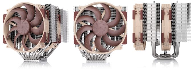
Noctua offers the NH-D15 G2 in three versions to address the specific requirements of modern CPUs. The regular version is versatile and can be used for AMD's AM5 processors and Intel's LGA1700 CPUs with included mounting accessories. The HBC (High Base Convexity) variant is tailored for LGA1700 processors, especially those subjected to full ILM pressure or those that have deformed over time, ensuring excellent contact quality despite the concave shape of the CPU. Finally, the LBC (Low Base Convexity) version is tailored for flat rectangular CPUs, providing optimal contact on AMD's AM5 and other similar processors.
While there are three versions of NH-D15 G2 aimed at different processors, they are all said to be compatible with a wide range of motherboards and other hardware. The new coolers' offset construction ensures clearance for the top PCIe x16 slot on most current motherboards. Additionally, they feature the upgraded Torx-based SecuFirm2+ multi-socket mounting system and come with Noctua's NT-H2 thermal compound.
For those looking to upgrade existing coolers like the NH-D15, NH-D15S, or NH-U14S series, Noctua is also releasing the NF-A14x25r G2 fans separately. These round-frame fans are fine-tuned in single and dual fan packages to minimize noise levels while offering decent cooling performance.
Finally, Noctua is also prepping a square-frame version of the NF-A14x25 G2 fan for release in September. This variant targets water-cooling radiators and case-cooling applications and promises to extend the versatility of Noctua's cooling solutions further.
All versions of Noctua's NH-D15 G2 coolers cost $149.90/€149.90. One NF-A14x25 G2 fan costs $39.90/€39.90, whereas a package of two fans costs $79.80/€79.80. The cooler is backed with a six-year warranty.
Cases/Cooling/PSUs' class='post-thumb' src='https://lh3.googleusercontent.com/blogger_img_proxy/AEn0k_uuaaO9irbJfQ1taNTC8O9ROatynoUDjRm4cNuwiq6Cjh02ttlU2Jg6nEYtUJS2ffwXCxsyzEs1RSGNjRJ85YDGHublEw63jc-a0sy4YYdVTeZo8MQqqSW0CkRbAT9sn8yjCszgcQ=w72-h72-p-k-no-nu'/>Noctua Launches New Flagship Cooler: NH-D15 G2 with LGA1851 CPUs Support
On Tuesday, Noctua introduced its second-generation NH-D15 cooler, which offers refined performance and formally supports Intel's next-generation Arrow Lake-S processors in LGA1851 packaging. Alongside its NH-D15 G2 CPU cooler, Noctua also introduced its NF-A14x25r G2 140mm fans.
The Noctua NH-D15 G2 is an enhanced version of the popular NH-D15 cooler with eight heat pipes, two asymmetrical fin-stack and two speed-offset 140-mm PWM fans (to avoid acoustic interaction phenomena such as periodic humming or intermittent vibrations). According to the manufacturer, these key components are tailored to work efficiently together to deliver superior quiet cooling performance, rivalling many all-in-one water cooling systems and pushing the boundaries of air cooling efficiency.
Noctua offers the NH-D15 G2 in three versions to address the specific requirements of modern CPUs. The regular version is versatile and can be used for AMD's AM5 processors and Intel's LGA1700 CPUs with included mounting accessories. The HBC (High Base Convexity) variant is tailored for LGA1700 processors, especially those subjected to full ILM pressure or those that have deformed over time, ensuring excellent contact quality despite the concave shape of the CPU. Finally, the LBC (Low Base Convexity) version is tailored for flat rectangular CPUs, providing optimal contact on AMD's AM5 and other similar processors.
While there are three versions of NH-D15 G2 aimed at different processors, they are all said to be compatible with a wide range of motherboards and other hardware. The new coolers' offset construction ensures clearance for the top PCIe x16 slot on most current motherboards. Additionally, they feature the upgraded Torx-based SecuFirm2+ multi-socket mounting system and come with Noctua's NT-H2 thermal compound.
For those looking to upgrade existing coolers like the NH-D15, NH-D15S, or NH-U14S series, Noctua is also releasing the NF-A14x25r G2 fans separately. These round-frame fans are fine-tuned in single and dual fan packages to minimize noise levels while offering decent cooling performance.
Finally, Noctua is also prepping a square-frame version of the NF-A14x25 G2 fan for release in September. This variant targets water-cooling radiators and case-cooling applications and promises to extend the versatility of Noctua's cooling solutions further.
All versions of Noctua's NH-D15 G2 coolers cost $149.90/€149.90. One NF-A14x25 G2 fan costs $39.90/€39.90, whereas a package of two fans costs $79.80/€79.80. The cooler is backed with a six-year warranty.
Cases/Cooling/PSUsKioxia Demonstrates RAID Offload Scheme for NVMe Drives
At FMS 2024, Kioxia had a proof-of-concept demonstration of their proposed a new RAID offload methodology for enterprise SSDs. The impetus for this is quite clear: as SSDs get faster in each generation, RAID arrays have a major problem of maintaining (and scaling up) performance. Even in cases where the RAID operations are handled by a dedicated RAID card, a simple write request in, say, a RAID 5 array would involve two reads and two writes to different drives. In cases where there is no hardware acceleration, the data from the reads needs to travel all the way back to the CPU and main memory for further processing before the writes can be done.
Kioxia has proposed the use of the PCIe direct memory access feature along with the SSD controller's controller memory buffer (CMB) to avoid the movement of data up to the CPU and back. The required parity computation is done by an accelerator block resident within the SSD controller.
In Kioxia's PoC implementation, the DMA engine can access the entire host address space (including the peer SSD's BAR-mapped CMB), allowing it to receive and transfer data as required from neighboring SSDs on the bus. Kioxia noted that their offload PoC saw close to 50% reduction in CPU utilization and upwards of 90% reduction in system DRAM utilization compared to software RAID done on the CPU. The proposed offload scheme can also handle scrubbing operations without taking up the host CPU cycles for the parity computation task.
Kioxia has already taken steps to contribute these features to the NVM Express working group. If accepted, the proposed offload scheme will be part of a standard that could become widely available across multiple SSD vendors.
StorageAMD Delays Ryzen 9000 Launch 1 to 2 Weeks Due to Chip Quality Issues
AMD sends word this afternoon that the company is delaying the launch of their Ryzen 9000 series desktop processors. The first Zen 5 architecture-based desktop chips were slated to launch next week, on July 31st. But citing quality issues that are significant enough that AMD is even pulling back stock already sent to distributors, AMD is delaying the launch by one to two weeks. The Ryzen 9000 launch will now be a staggered launch, with the Ryzen 5 9600X and Ryzen 7 9700X launching on August 8th, while the Ryzen 9 9900X and flagship Ryzen 9 9950X will launch a week after that, on August 15th.
The exceptional announcement, officially coming from AMD’s SVP and GM of Computing and Graphics, Jack Huynh, is short and to the point. Ahead of the launch, AMD found that “the initial production units that were shipped to our channel partners did not meet our full quality expectations.” And, as a result, the company has needed to delay the launch in order to rectify the issue.
Meanwhile, because AMD had already distributed chips to their channel partners – distributors who then filter down to retailers and system builders – this is technically a recall as well, as AMD needs to pull back the first batch of chips and replace them with known good units. That AMD has to essentially take a do-over on initial chip distribution is ultimately what’s driving this delay; it takes the better part of a month to properly seed retailers for a desktop CPU launch with even modest chip volumes, so AMD has to push the launch out to give their supply chain time to catch up.
For the moment, there are no further details on what the quality issue with the first batch of chips is, how many are affected, or what any kind of fix may entail. Whatever the issue is, AMD is simply taking back all stock and replacing it with what they’re calling “fresh units.”
| AMD Ryzen 9000 Series Processors Zen 5 Microarchitecture (Granite Ridge) |
||||||||
| AnandTech | Cores / Threads |
Base Freq |
Turbo Freq |
L2 Cache |
L3 Cache |
Memory Support | TDP | Launch Date |
| Ryzen 9 9950X | 16C/32T | 4.3GHz | 5.7GHz | 16 MB | 64 MB | DDR5-5600 | 170W | 08/15 |
| Ryzen 9 9900X | 12C/24T | 4.4GHz | 5.6GHz | 12 MB | 64 MB | 120W | ||
| Ryzen 7 9700X | 8C/16T | 3.8GHz | 5.5GHz | 8 MB | 32 MB | 65W | 08/08 | |
| Ryzen 5 9600X | 6C/12T | 3.9GHz | 5.4GHz | 6 MB | 32 MB | 65W | ||
Importantly, however, this announcement is only for the Ryzen 9000 desktop processors, and not the Ryzen AI 300 mobile processors (Strix Point), which are still slated to launch next week. A mobile chip recall would be a much bigger issue (they’re in finished devices that would need significant labor to rework), but also, both the new desktop and mobile Ryzen processors are being made on the same TSMC N4 process node, and have significant overlap due to their shared use of the Zen 5 architecture. To be sure, mobile and desktop are very different dies, but it does strongly imply that whatever the issue is, it’s not a design flaw or a fabrication flaw in the silicon itself.
That AMD is able to re-stage the launch of the desktop Ryzen 9000 chips so quickly – on the order of a few weeks – further points to an issue much farther down the line. If indeed the issue isn’t at the silicon level, then that leaves packaging and testing as the next most likely culprit. Whether that means AMD’s packaging partners had some kind of issue assembling the multi-die chips, or if AMD found some other i... CPUs
ASRock Unveils Motherboards For Ryzen 9000 At Computex 2024: X870E Taichi and X870E Taichi Lite
During Computex 2024, ASRock held an event to unveil some of its upcoming X870E motherboards, designed for AMD's Zen 5-based Ryzen 9000 series processors. ASRock's announcement includes a pair of Taichi-branded boards, the X870E Taichi and the lighter X870E Taichi lite, which uses AMD's X870E (Promontory 21) chipset for AM5.
The current flagship model announced from ASRock's X870E line-up for Ryzen 9000 is the ASRock X870E Taichi. ASRock is advertising a large 27-phase power delivery through 110A SPS, suggesting this board is designed for overclockers and all-around power users. Two PCIe 5.0 x16 slots (operating in either x16/x0 or x8/x8) provide high-speed bandwidth for cutting-edge graphics cards and other devices. Meanwhile, ASRock has gone with 4 DIMM slots on this board, so system builders will be able to max out the board's memory capacity at the cost of bandwidth.
The storage offering is impressive; besides the obligatory PCIe Gen5 x4 M.2 slot (Blazing M.2), ASRock has outfit the board with another three PCIe Gen4 x4 (Hyper) M.2 slots. Also present are two USB4 Type-C ports for high-bandwidth external I/O, while networking support is a solid pairing of a discrete Wi-Fi 7 controller with a Realtek 5Gb Ethernet controller (and the first AM5 board we've come across with something faster than a 2.5GbE controller).
The audio setup includes a Realtek ALC4082 codec and ESS SABRE9218 DAC supporting high-fidelity sound. The BIOS flashback feature is also a nice touch, and we believe this should be a feature on all mid-range to high-end motherboards, which provides an easy way to update the firmware without installing a CPU. And, as no high-end board would be complete without it, ASRock has put RGB lighting on the X870E Taichi as well.
Ultimately, as ASRock's high-end X870E board, the X870E Taichi comes with pretty much every last cutting-edge technology that ASRock can fit on the board.
Comparatively, the ASRock X870E Taichi Lite is a more streamlined and functional version of the X870E Taichi. The Lite retaining all of the latter's key features, including the 27-phase power delivery with 110A smart power stages, dual PCIe 5.0 x16 slots operating at x16 or x8/x8, four DDR5 DIMM slots, and four M.2 slots (1x Gen5 + 3x Gen4). The only significant difference is aesthetics: the Taichi Lite features a simpler silver-themed design without the RGB lighting, while the standard Taichi has a more intricate gold-accented and fanciful aesthetics.
In terms of availability, ASRock is not disclosing a release date for the board at the show. And, checking around with other tech journalists, Andreas Schilling from HawrdwareLUXX has heard that X870E and X870 motherboards aren't expected to be available in time for the Ryzen 9000 series launch. We will investigate this and contact the motherboard vendors to confirm the situation. Though as X870E/X870 boards barely differ from the current crop of X670E/B650E boards to begin with, the Ryzen 9000 series won't be fazed by a lack of slightly newer motherboards.
MotherboardsTags
- https://www.amazon.com/2020-2021-Planner-Academic-Do-Twin-Wire/dp/B083V11TM5?tag=all0ad0-21https://m.media-amazon.com/images/I/41btLRSWksL.jpg
- https://www.amazon.com/Acid-Dreams-Complete-History-Sixties-ebook/dp/B005012G6U?tag=all0ad0-21https://m.media-amazon.com/images/I/51SwQkWyzAL.jpg
- https://www.amazon.com/Adaptive-Charging-Charger-Compatible-EP-TA20JBE/dp/B07NPD5T5H?tag=all0ad0-21https://m.media-amazon.com/images/I/419ZKbzdOwL.jpg
- https://www.amazon.com/Adjustable-Foldable-Portable-Compatible-Smartphones/dp/B0963PBY4C?tag=all0ad0-21https://m.media-amazon.com/images/I/51p4wF13kCL.jpg
- https://www.amazon.com/African-Twisted-Headwraps-Headband-Headscarf/dp/B09FDMKTZP?tag=all0ad0-21https://m.media-amazon.com/images/I/41WGbzL+RkL.jpg
- https://www.amazon.com/AINOPE-Charging-Braided-compatible-MacBook/dp/B094YDZQ1C?tag=all0ad0-21https://m.media-amazon.com/images/I/51ppc0xIVtL.jpg
- https://www.amazon.com/Ambergris-Saints-Madmen-Shriek-Finch/dp/B08GGCSN3S?tag=all0ad0-21https://m.media-amazon.com/images/I/51zgVCTiUiL.jpg
- https://www.amazon.com/Amplim-Hospital-Thermometer-Professional-Thermometer/dp/B0865R5H82?tag=all0ad0-21https://m.media-amazon.com/images/I/31K01H4s6UL.jpg
- https://www.amazon.com/Animal-Gaming-Electronic-Lights-Birthday/dp/B0B2QTLWMS?tag=all0ad0-21https://m.media-amazon.com/images/I/41GY22qHwkL.jpg
- https://www.amazon.com/Animals-Flashcards-Children-Alphabet-cards/dp/9811168881?tag=all0ad0-21https://m.media-amazon.com/images/I/51U2gcSb62L.jpg
- https://www.amazon.com/ANNKIE-Dance-Electronic-Lights-Birthday/dp/B0B74DVQQV?tag=all0ad0-21https://m.media-amazon.com/images/I/51K45aP99DL.jpg
- https://www.amazon.com/Anti-Wrinkle-Silicone-Reusable-D%C3%A9collet%C3%A9-Eliminate/dp/B07FQ3QV1C?tag=all0ad0-21https://m.media-amazon.com/images/I/41RhHEsEi3L.jpg
- https://www.amazon.com/anyloop-Military-Smartwatch-Bluetooth-Waterproof/dp/B0C4P7R6CK?tag=all0ad0-21https://m.media-amazon.com/images/I/41lUAHTmi5L.jpg
- https://www.amazon.com/Aromatherapy-Shower-Steamers-Relaxation-Everything/dp/B08QDKWBWS?tag=all0ad0-21https://m.media-amazon.com/images/I/613KwmLJJ1L.jpg
- https://www.amazon.com/Audible-A-Rose-in-Winter/dp/B09JHTGT14?tag=all0ad0-21https://m.media-amazon.com/images/I/51z1bVj4CxL.jpg
- https://www.amazon.com/Audible-Fall-School-Good-Evil/dp/B0B8SZY3P5?tag=all0ad0-21https://m.media-amazon.com/images/I/51MWO0bOLIL.jpg
- https://www.amazon.com/Audible-Termination-Shock-A-Novel/dp/B09556Y79B?tag=all0ad0-21https://m.media-amazon.com/images/I/51jEsfJXG3S.jpg
- https://www.amazon.com/Automatic-Toddlers-Operated-Batteries-Birthday/dp/B0BZH34G2G?tag=all0ad0-21https://m.media-amazon.com/images/I/51PQaTAouaL.jpg
- https://www.amazon.com/AWGOU-Baby-Wipes-Dispenser-Large-Capacity/dp/B0BS3K9BFV?tag=all0ad0-21https://m.media-amazon.com/images/I/41emlsr6WnL.jpg
- https://www.amazon.com/AYAO-Blades-8-Inch-12TPI-2-Pack/dp/B0C9C1VB3D?tag=all0ad0-21https://m.media-amazon.com/images/I/41jMumgfJ4L.jpg
- https://www.amazon.com/Backless-Sleeve-Ribbed-Fitted-Shirts/dp/B0B68KPGP8?tag=all0ad0-21https://m.media-amazon.com/images/I/41vB0uLnuzL.jpg
- https://www.amazon.com/BCHWAY-Stuffed-Storage-Beanbag-Organizer/dp/B09WR2KPPG?tag=all0ad0-21https://m.media-amazon.com/images/I/41GBr+1tEBL.jpg
- https://www.amazon.com/beeprt-Bluetooth-Shipping-Label-Printer/dp/B0BK93ZSNC?tag=all0ad0-21https://m.media-amazon.com/images/I/41Ufm05KrJL.jpg
- https://www.amazon.com/Benewid-Creami-Pints-Lids-Containers/dp/B0C85Q44N6?tag=all0ad0-21https://m.media-amazon.com/images/I/41bFv6o0xjL.jpg
- https://www.amazon.com/BIG-TEETH-Magnetic-Microfiber-5-Piece/dp/B0BRXBM2T9?tag=all0ad0-21https://m.media-amazon.com/images/I/51BCt4B8jDL.jpg
- https://www.amazon.com/Blackbeard-Americas-Most-Notorious-Pirate/dp/B086N4X4SG?tag=all0ad0-21https://m.media-amazon.com/images/I/51fqeuICW+L.jpg
- https://www.amazon.com/Blaster-Automatic-Toddlers-Christmas-Birthday/dp/B0CCV9RDM5?tag=all0ad0-21https://m.media-amazon.com/images/I/51j8FkZtBiL.jpg
- https://www.amazon.com/Bloodline-Jess-Lourey/dp/1542016312?tag=all0ad0-21https://m.media-amazon.com/images/I/51KLqBsOIbL.jpg
- https://www.amazon.com/Bracelet-Stainless-Zirconium-Ceramic-Statement/dp/B0B2CQR5YW?tag=all0ad0-21https://m.media-amazon.com/images/I/41iUmnfsAmL.jpg
- https://www.amazon.com/Bride-Shadow-King-Book/dp/B0B75RL7DX?tag=all0ad0-21https://m.media-amazon.com/images/I/51LyIt-n5+L.jpg
- https://www.amazon.com/Bright-Empires-House-Spirit-Shadow/dp/B08T4VG1S2?tag=all0ad0-21https://m.media-amazon.com/images/I/61-JxjVNClL.jpg
- https://www.amazon.com/BRIGHTWORLD-Stuffers-Upgrade-5-9inch-Birthday/dp/B0B6RBCYZ7?tag=all0ad0-21https://m.media-amazon.com/images/I/61pQaIf3NVL.jpg
- https://www.amazon.com/Bunfly-Clipper-Grooming-Suction-Capacity/dp/B0C6PMSY3Z?tag=all0ad0-21https://m.media-amazon.com/images/I/51ig7m1g9OL.jpg
- https://www.amazon.com/C412H-Spring-Wound-Commercial-12-Hour-Automatic/dp/B00CTW2LYA?tag=all0ad0-21https://m.media-amazon.com/images/I/41QNVA+3MRL.jpg
- https://www.amazon.com/Cardone-Select-84-832-Ignition-Distributor/dp/B000CFFAYY?tag=all0ad0-21https://m.media-amazon.com/images/I/414iGfzryML.jpg
- https://www.amazon.com/ceiba-tree-Graduation-Envelopes-Classroom/dp/B0BQQKSLFK?tag=all0ad0-21https://m.media-amazon.com/images/I/51ZOS4YOvzL.jpg
- https://www.amazon.com/CellElection-Elastic-Ponytail-Holders-Straight/dp/B09TFDLR85?tag=all0ad0-21https://m.media-amazon.com/images/I/514QbooGKKL.jpg
- https://www.amazon.com/Certified-Charger-Charging-Braveridge-Lightning/dp/B0C1VKRXN1?tag=all0ad0-21https://m.media-amazon.com/images/I/41XG+lopk8L.jpg
- https://www.amazon.com/Certified%E3%80%91-Charger-Fasting-Charging-Compatible/dp/B0C489SXGB?tag=all0ad0-21https://m.media-amazon.com/images/I/41dNzZS3BML.jpg
- https://www.amazon.com/Charger-Certified-Lightning-Charging-Compatible/dp/B0C4L9S7QH?tag=all0ad0-21https://m.media-amazon.com/images/I/514iP4Fy28L.jpg
- https://www.amazon.com/Chicken-Shredder-Ergonomic-Anti-Slip-Dishwasher/dp/B0C5R1KZP6?tag=all0ad0-21https://m.media-amazon.com/images/I/61cx6f737WL.jpg
- https://www.amazon.com/Christmas-Decorations-PHITRIC-Sparkling-Fireplace/dp/B0B7WNC93J?tag=all0ad0-21https://m.media-amazon.com/images/I/51Gv07W+JCL.jpg
- https://www.amazon.com/Christmas-Snowflake-Stamping-Manicure-Designer/dp/B09L4SV5YY?tag=all0ad0-21https://m.media-amazon.com/images/I/51TQJxPWLrL.jpg
- https://www.amazon.com/Cleaning-Bathroom-Crevice-Bristle-Multifunctional/dp/B0CDBK4C9T?tag=all0ad0-21https://m.media-amazon.com/images/I/415dsUeaDmL.jpg
- https://www.amazon.com/Clinic-Crohns-Disease-Ulcerative-Colitis-ebook/dp/B09ZBLJLFL?tag=all0ad0-21https://m.media-amazon.com/images/I/41f5FHJle+L.jpg
- https://www.amazon.com/Coasters-Absorbent-Ceramic-Coaster-Housewarming/dp/B09ZKJRSLH?tag=all0ad0-21https://m.media-amazon.com/images/I/51POqbEgyOL.jpg
- https://www.amazon.com/CoBak-Rotating-Case-iPad-Generation/dp/B0BBR8MFHM?tag=all0ad0-21https://m.media-amazon.com/images/I/516NR1N0QKL.jpg
- https://www.amazon.com/COLORFULLEAF-Bamboo-Underwear-Breathable-Trunks/dp/B0B9BX5S9L?tag=all0ad0-21https://m.media-amazon.com/images/I/31MYPhHHapL.jpg
- https://www.amazon.com/Comforter-Paisley-Microfiber-Bohemian-Pillowcases/dp/B0BZP1SC6F?tag=all0ad0-21https://m.media-amazon.com/images/I/51KkoN3AgNL.jpg
- https://www.amazon.com/Compressed-Cordless-Electric-Brushless-Portable/dp/B0BBR1XHLS?tag=all0ad0-21https://m.media-amazon.com/images/I/41dJ2sJpGjL.jpg
- https://www.amazon.com/Cordking-14-Protectors-Shockproof-Microfiber/dp/B0B6GKRCGM?tag=all0ad0-21https://m.media-amazon.com/images/I/41tXMeWi5FL.jpg
- https://www.amazon.com/Cordless-High-Speed-Brushless-Lightweight-Cleaners/dp/B0CGL8NBM8?tag=all0ad0-21https://m.media-amazon.com/images/I/41NfsXSEnLL.jpg
- https://www.amazon.com/Cordless-Straightening-Travel-Wireless-Straightener/dp/B0CJ2HQL3H?tag=all0ad0-21https://m.media-amazon.com/images/I/31wTmdUZyuL.jpg
- https://www.amazon.com/Corrector-Clavicle-Adjustable-Straightener-Providing/dp/B07L41CV8B?tag=all0ad0-21https://m.media-amazon.com/images/I/41B0xbK2kRL.jpg
- https://www.amazon.com/Court-Wizard-Terry-Mancour-audiobook/dp/B07PC2RQSC?tag=all0ad0-21https://m.media-amazon.com/images/I/512jFQbt6JL.jpg
- https://www.amazon.com/Cozivwaiy-Platform-Sandals-Studded-Evening/dp/B0BM43W7VF?tag=all0ad0-21https://m.media-amazon.com/images/I/41+RFM1gP7L.jpg
- https://www.amazon.com/Crenova-Magnetic-Construction-Preschool-Educational/dp/B0CC1RZ2BJ?tag=all0ad0-21https://m.media-amazon.com/images/I/51lJxAlaL3L.jpg
- https://www.amazon.com/Dan-Darci-Marbling-Paint-Kids/dp/B08CLVVJ8C?tag=all0ad0-21https://m.media-amazon.com/images/I/61nDIOC0B0L.jpg
- https://www.amazon.com/Dash-Cam-Front-BOOGIIO-Dashboard/dp/B08LZJ8GMH?tag=all0ad0-21https://m.media-amazon.com/images/I/41B3QK42N1L.jpg
- https://www.amazon.com/Democracy-America-What-Wrong-About-ebook/dp/B0867TRV52?tag=all0ad0-21https://m.media-amazon.com/images/I/4129LSadlmL.jpg
- https://www.amazon.com/Detailing-Attachment-Scrubber-Cleaning-Upholstery/dp/B07WGKQVN7?tag=all0ad0-21https://m.media-amazon.com/images/I/41K75BhGaML.jpg
- https://www.amazon.com/Diameter-Hydrophilic-Filtration-Non-sterile-COBETTER/dp/B0B7BB3L1R?tag=all0ad0-21https://m.media-amazon.com/images/I/31KD4E7TW5L.jpg
- https://www.amazon.com/Diamond-Organizer-Jewelry-Storage-Diamonds/dp/B08JLVSZ15?tag=all0ad0-21https://m.media-amazon.com/images/I/514Z+bbZfQL.jpg
- https://www.amazon.com/Diamond-Painting-Diamonds-12x16inch-30%C3%9740cm/dp/B09X1CQJHX?tag=all0ad0-21https://m.media-amazon.com/images/I/51xEpqCkI-L.jpg
- https://www.amazon.com/didforu-Monocular-Telescope-Monoscope-Binocular/dp/B0C3757D5G?tag=all0ad0-21https://m.media-amazon.com/images/I/512qer0p1oL.jpg
- https://www.amazon.com/Dinkhiiro-Outdoor-Pickleball-Balls-Pickle-Ball-Accessories-Pickleball/dp/B0BNQ8HM76?tag=all0ad0-21https://m.media-amazon.com/images/I/41ni+GPR71L.jpg
- https://www.amazon.com/Distant-Horizon-Backyard-Starship-Book/dp/B0BDP9RPQL?tag=all0ad0-21https://m.media-amazon.com/images/I/512FYS+c9wL.jpg
- https://www.amazon.com/Dorman-1650134-Chevrolet-Driver-Assembly/dp/B00JW1XGDG?tag=all0ad0-21https://m.media-amazon.com/images/I/51p-ja2Vc9L.jpg
- https://www.amazon.com/DosTutu-Mermaid-Costume-Pageant-Birthday/dp/B09NJK6K9M?tag=all0ad0-21https://m.media-amazon.com/images/I/51pVYQBZKJL.jpg
- https://www.amazon.com/dp/B09GFWPXWH?tag=all0ad0-21https://m.media-amazon.com/images/I/51xO7ZL-sVL.jpg
- https://www.amazon.com/DREAMS-VISIONS-Jesus-Awakening-Muslim-ebook/dp/B0078FAA3M?tag=all0ad0-21https://m.media-amazon.com/images/I/51BKVftuXDL.jpg
- https://www.amazon.com/DSJUGGLING-Transparent-Two-Tone-Juggling-Beginners/dp/B09WHRZCFF?tag=all0ad0-21https://m.media-amazon.com/images/I/419NOeSGijL.jpg
- https://www.amazon.com/Empire-of-Storms-Sarah-J-Maas-audiobook/dp/B01KIQV5EU?tag=all0ad0-21https://m.media-amazon.com/images/I/51EMceUgxFL.jpg
- https://www.amazon.com/Eniucow-Montessori-Permanent-Traction-Toddlers/dp/B0B7CZ9KGN?tag=all0ad0-21https://m.media-amazon.com/images/I/31bJyZYqhJL.jpg
- https://www.amazon.com/Eslazoer-insulated-neoprene-reusable-activity/dp/B0BKSMXVN8?tag=all0ad0-21https://m.media-amazon.com/images/I/41kTXH2JxBL.jpg
- https://www.amazon.com/Everyday-Solutions-Mug-Tree-Polished/dp/B0B4T6NCML?tag=all0ad0-21https://m.media-amazon.com/images/I/31-7RTd1fUL.jpg
- https://www.amazon.com/Extender-Universal-Rotatable-Extension-Attachment/dp/B0C4YLVH3D?tag=all0ad0-21https://m.media-amazon.com/images/I/41+YysChcFL.jpg
- https://www.amazon.com/Eyelash-Extension-Cleanser-BREYLEE-Shampoo/dp/B08RJFTFN4?tag=all0ad0-21https://m.media-amazon.com/images/I/51UncwwSzwL.jpg
- https://www.amazon.com/Fatal-Discord-Michael-Massing-audiobook/dp/B078YDCMBD?tag=all0ad0-21https://m.media-amazon.com/images/I/51AJdROll+L.jpg
- https://www.amazon.com/Faucet-Sprayer-Attachment-Replacement-included/dp/B0BCFMT7WY?tag=all0ad0-21https://m.media-amazon.com/images/I/31wZDbk-bYL.jpg
- https://www.amazon.com/Feeling-Good-David-D-Burns-audiobook/dp/B01N9TCVLD?tag=all0ad0-21https://m.media-amazon.com/images/I/51ixV6lf9AL.jpg
- https://www.amazon.com/FeelinGirl-Waitsted-Shapewear-Control-Lifting/dp/B0CBK29G76?tag=all0ad0-21https://m.media-amazon.com/images/I/31Cl6qaK0HL.jpg
- https://www.amazon.com/Fenceguru-Decorative-Rustproof-Barrier-Landscape/dp/B0BZ91ZPHF?tag=all0ad0-21https://m.media-amazon.com/images/I/519kGS3sjxL.jpg
- https://www.amazon.com/Fernco-PQC-105-Flexible-Reusable-Plastic/dp/B00CFVNCCK?tag=all0ad0-21https://m.media-amazon.com/images/I/21xcHMaS37L.jpg
- https://www.amazon.com/Floating-Shelves-Bathroom-Bedroom-Kitchen/dp/B0CF8J497J?tag=all0ad0-21https://m.media-amazon.com/images/I/51cT9HpSh4L.jpg
- https://www.amazon.com/Forehead-Thermometer-Infrared-Eligible-Indicator/dp/B0B4ZD6K43?tag=all0ad0-21https://m.media-amazon.com/images/I/31J97vQVUHL.jpg
- https://www.amazon.com/FRGROW-Lights-Spectrum-Function-Gooseneck/dp/B0CC4P13L7?tag=all0ad0-21https://m.media-amazon.com/images/I/51UXtap-56L.jpg
- https://www.amazon.com/Funrous-Mattress-Lifter-Helper-Stainless/dp/B09WMZPM1N?tag=all0ad0-21https://m.media-amazon.com/images/I/31Vg6rJibzL.jpg
- https://www.amazon.com/GAOY-Glassy-Foundation-Combination-Polish/dp/B0BD4MMFVM?tag=all0ad0-21https://m.media-amazon.com/images/I/414wIShbm+L.jpg
- https://www.amazon.com/Gay-Pride-Rainbow-Heart-Silicone/dp/B01J8E5NUA?tag=all0ad0-21https://m.media-amazon.com/images/I/31TtNjUl3uL.jpg
- https://www.amazon.com/Gerod-Compatible-Replacement-Cushions-Headphones/dp/B09BPV34ZB?tag=all0ad0-21https://m.media-amazon.com/images/I/41cXXPmWNoL.jpg
- https://www.amazon.com/GetKen-Dispenser-Rechargeable-Portable-Automatic/dp/B0C4T26LK4?tag=all0ad0-21https://m.media-amazon.com/images/I/41v5jE7AsIL.jpg
- https://www.amazon.com/Gifts-Girls-birthday-Toys-Duplication/dp/B0B6FY328P?tag=all0ad0-21https://m.media-amazon.com/images/I/51mMmkuwdfL.jpg
- https://www.amazon.com/Girls-Charm-Bracelet-Making-Kit/dp/B0CFCC8HBZ?tag=all0ad0-21https://m.media-amazon.com/images/I/81-SB1q4h1L.jpg
- https://www.amazon.com/Girls-Charm-Bracelet-Making-Kit/dp/B0CFF3SLJT?tag=all0ad0-21https://m.media-amazon.com/images/I/81kJ83iM+IL.jpg
- https://www.amazon.com/GloFX-Blue-Rave-Bedroom-Decor/dp/B0B7ZXG6PS?tag=all0ad0-21https://m.media-amazon.com/images/I/41iPdpfs1DL.jpg
- https://www.amazon.com/GMSOL-Diamond-Necklaces-Necklace-Layered/dp/B0BXKY3XW9?tag=all0ad0-21https://m.media-amazon.com/images/I/21iQgpW3i4L.jpg
- https://www.amazon.com/Greenland-Home-GL-THROWSH-Shangri-La-Throw/dp/B017U6U8JO?tag=all0ad0-21https://m.media-amazon.com/images/I/61VISLraXWL.jpg
- https://www.amazon.com/Gyierwe-High-Pressure-Stainless-Adjustable-Filtration/dp/B0C5RHCSN8?tag=all0ad0-21https://m.media-amazon.com/images/I/51RZ3tTLzyL.jpg
- https://www.amazon.com/Halloween-Decorations-Indoor-DECSPAS-Haunted/dp/B0C6JPZ6K5?tag=all0ad0-21https://m.media-amazon.com/images/I/51zSmWVx7HL.jpg
- https://www.amazon.com/HawSkgFub-Curtains-Farmhouse-Seasonal-Bathroom/dp/B0BVLTJR4P?tag=all0ad0-21https://m.media-amazon.com/images/I/412k-TN9yzL.jpg
- https://www.amazon.com/Helping-Soldering-Hand-Base-Microscope/dp/B0BBR46ZQ9?tag=all0ad0-21https://m.media-amazon.com/images/I/41IZoepkAkL.jpg
- https://www.amazon.com/Her-Soul-Take-Souls-Trilogy/dp/B0BDT2M2QZ?tag=all0ad0-21https://m.media-amazon.com/images/I/51Z1AUkTytL.jpg
- https://www.amazon.com/HISANDUK-Pendant-Fixtures-Kitchen-Adjustable/dp/B0B76G6VCT?tag=all0ad0-21https://m.media-amazon.com/images/I/41SzQX+tAeL.jpg
- https://www.amazon.com/Homeleo-Operated-Christmas-Strawberry-Decorations/dp/B07WTVGTWX?tag=all0ad0-21https://m.media-amazon.com/images/I/51+CNn9QowL.jpg
- https://www.amazon.com/House-of-Impossible-Beauties-audiobook/dp/B077VQ68HH?tag=all0ad0-21https://m.media-amazon.com/images/I/51VFkDIrDsL.jpg
- https://www.amazon.com/HOUSE-Organizer-Upgraded-Undersink-Organizers/dp/B0BY8XZK71?tag=all0ad0-21https://m.media-amazon.com/images/I/510FKKVDhpL.jpg
- https://www.amazon.com/House-Witch-Humorous-Romantic-Fantasy/dp/B0BLJ7CQKK?tag=all0ad0-21https://m.media-amazon.com/images/I/61+JJSw9jZL.jpg
- https://www.amazon.com/HR-Quadcopter-Beginners-Altitude-Batteries/dp/B08L8YFT4S?tag=all0ad0-21https://m.media-amazon.com/images/I/41pf-DNDj5L.jpg
- https://www.amazon.com/Humble-Chic-Wall-Art-Prints/dp/B07QL3GTX4?tag=all0ad0-21https://m.media-amazon.com/images/I/31QO1OLNDGL.jpg
- https://www.amazon.com/Huyerdo-Corduroy-Cosmetic-Aesthetic-Organizer/dp/B0C1YXPX5M?tag=all0ad0-21https://m.media-amazon.com/images/I/51Es7IjWzjL.jpg
- https://www.amazon.com/I-Invited-Her-In-Adele-Parks-audiobook/dp/B07JZGFFHY?tag=all0ad0-21https://m.media-amazon.com/images/I/51ak3gyHziL.jpg
- https://www.amazon.com/In1docom-Peanut-Massage-Massager-Lacrosse/dp/B0CB4S2JRX?tag=all0ad0-21https://m.media-amazon.com/images/I/41sBnhqhZzL.jpg
- https://www.amazon.com/INeedIt-D101-Portable-Wireless-Organization/dp/B0BCKV8B81?tag=all0ad0-21https://m.media-amazon.com/images/I/21OGF1G7x9L.jpg
- https://www.amazon.com/Inflatable-Ground-Dustproof-Rainproof-Waterproof/dp/B0CB8B4PKX?tag=all0ad0-21https://m.media-amazon.com/images/I/51o0yuVrjPL.jpg
- https://www.amazon.com/Insane-Labz-Bitartrate-AMPiberry-Endurance/dp/B07V6JCWJG?tag=all0ad0-21https://m.media-amazon.com/images/I/51GZtu2lUZL.jpg
- https://www.amazon.com/Island-Queen-A-Novel/dp/B08MLPY619?tag=all0ad0-21https://m.media-amazon.com/images/I/51snO62ltvL.jpg
- https://www.amazon.com/J-hong-Toddlers-Learning-Montessori-Christmas/dp/B0C4LK67Q5?tag=all0ad0-21https://m.media-amazon.com/images/I/51q4mMYfoLL.jpg
- https://www.amazon.com/jalz-Wooden-Spoons-Cooking-3-Piece/dp/B07DZKTC9B?tag=all0ad0-21https://m.media-amazon.com/images/I/416iXJ1B8PL.jpg
- https://www.amazon.com/JENN-ARDOR-Fashion-Sneakers-Comfortable/dp/B08N16X7HR?tag=all0ad0-21https://m.media-amazon.com/images/I/41y+m0CTBeS.jpg
- https://www.amazon.com/John-Sterling-Sports-7-Ball-Capacity/dp/B01DWSH1I0?tag=all0ad0-21https://m.media-amazon.com/images/I/31-O3z3v+XL.jpg
- https://www.amazon.com/Jorpet-Elevated-Adjustable-Non-Slip-Stainless/dp/B0C3YRH31J?tag=all0ad0-21https://m.media-amazon.com/images/I/41+P1DIyA0L.jpg
- https://www.amazon.com/JOYMODE-women-workout-clothes-Legging/dp/B08766FN91?tag=all0ad0-21https://m.media-amazon.com/images/I/31DoD7LD8EL.jpg
- https://www.amazon.com/Kettlebell-Whiskey-Shaped-Silicone-Melting/dp/B0C5NBXHDF?tag=all0ad0-21https://m.media-amazon.com/images/I/41XwetcdbXL.jpg
- https://www.amazon.com/Kingdom-Come-Backyard-Starship-Book/dp/B0BKBRDCV2?tag=all0ad0-21https://m.media-amazon.com/images/I/51DX-OPQv6L.jpg
- https://www.amazon.com/Kitchen-BAYZZ-Cushioned-Non-Slip-Waterproof/dp/B095GZYG7Z?tag=all0ad0-21https://m.media-amazon.com/images/I/41-vM6JlCeL.jpg
- https://www.amazon.com/KOIOS-Immersion-Multifunctional-Stainless-Titanium/dp/B076GW89V9?tag=all0ad0-21https://m.media-amazon.com/images/I/41YrmEtdu0L.jpg
- https://www.amazon.com/Lady-Orc-Sworn-Book/dp/B0B4BB9B21?tag=all0ad0-21https://m.media-amazon.com/images/I/51VsjpQ+WoL.jpg
- https://www.amazon.com/Large-Multipurpose-Waterproof-Picnic-Shopping/dp/B0CCS1HSMK?tag=all0ad0-21https://m.media-amazon.com/images/I/410kS6OJJHL.jpg
- https://www.amazon.com/Large-Multipurpose-Waterproof-Picnic-Shopping/dp/B0CF58TZ9J?tag=all0ad0-21https://m.media-amazon.com/images/I/410kS6OJJHL.jpg
- https://www.amazon.com/Lay-My-Heart-Angela-Pneuman-ebook/dp/B00FJ5EQ0Q?tag=all0ad0-21https://m.media-amazon.com/images/I/419DBRj4HuL.jpg
- https://www.amazon.com/LeadDock-Ice-Cube-Tray-Lid/dp/B0CB6TN9DY?tag=all0ad0-21https://m.media-amazon.com/images/I/51WpROdbWEL.jpg
- https://www.amazon.com/Learning-Educational-Preschool-Developmental-Montessori/dp/B0BY2HBQLS?tag=all0ad0-21https://m.media-amazon.com/images/I/510R2-67PbL.jpg
- https://www.amazon.com/LEDKINGDOMUS-inches-Driving-Compatible-Pickup/dp/B09176936Z?tag=all0ad0-21https://m.media-amazon.com/images/I/416I+aay3RL.jpg
- https://www.amazon.com/Legend-Randidly-Ghosthound-LitRPG-Adventure/dp/B09CR88G8L?tag=all0ad0-21https://m.media-amazon.com/images/I/51cte+pTRVL.jpg
- https://www.amazon.com/Legend-Randidly-Ghosthound-LitRPG-Adventure/dp/B09NB32VS5?tag=all0ad0-21https://m.media-amazon.com/images/I/51HquIJf4EL.jpg
- https://www.amazon.com/Legend-Randidly-Ghosthound-LitRPG-Adventure/dp/B09WTLH4Z9?tag=all0ad0-21https://m.media-amazon.com/images/I/61j-pJq9blL.jpg
- https://www.amazon.com/LENRUE-Computer-Speakers-Desktop-AUX_Black/dp/B0BRFN13S9?tag=all0ad0-21https://m.media-amazon.com/images/I/41XeSj+qShL.jpg
- https://www.amazon.com/LIANTRAL-Firewood-Outdoor-Upgrade-Fireplace/dp/B0BKSVRW4N?tag=all0ad0-21https://m.media-amazon.com/images/I/51Y9mIZmocL.jpg
- https://www.amazon.com/Lilys-White-Lace-Carolyn-Brown-ebook/dp/B00DTTW5UW?tag=all0ad0-21https://m.media-amazon.com/images/I/51iPZWUaUQL.jpg
- https://www.amazon.com/LISEN-Magnetic-Install-Friendly-Smartphones/dp/B07YRKDF4P?tag=all0ad0-21https://m.media-amazon.com/images/I/51tMoOMiRzL.jpg
- https://www.amazon.com/LJIOEZZI-Balaclava-Weather-Snowboarding-Motorcycling/dp/B0BHVNYM8Z?tag=all0ad0-21https://m.media-amazon.com/images/I/31YRjxzYi8L.jpg
- https://www.amazon.com/LOXP-2C-CAR-Sun-Shade-Umbrella-Medium/dp/B0BR7WLLY4?tag=all0ad0-21https://m.media-amazon.com/images/I/41vWPHUEsJL.jpg
- https://www.amazon.com/LUENX-Trendy-Oversized-Aviator-Sunglasses/dp/B09CMB5D7N?tag=all0ad0-21https://m.media-amazon.com/images/I/41uZsi7kskL.jpg
- https://www.amazon.com/MAGEFY-Eyelashes-Natural-Handmade-Reusable/dp/B0956V789H?tag=all0ad0-21https://m.media-amazon.com/images/I/51UgJTxfm2S.jpg
- https://www.amazon.com/Magnetic-Birthday-Building-Preschool-Montessori/dp/B0BWWPC5MR?tag=all0ad0-21https://m.media-amazon.com/images/I/61UuS8o90ZL.jpg
- https://www.amazon.com/Makartt-Extension-Glitter-Trendy-Builder/dp/B096VQW7NF?tag=all0ad0-21https://m.media-amazon.com/images/I/31hUzSIu6gL.jpg
- https://www.amazon.com/Makeup-Brush-Holder-Travel-Essentials/dp/B0C7G5YXRZ?tag=all0ad0-21https://m.media-amazon.com/images/I/31od+KNxUkL.jpg
- https://www.amazon.com/MaraFansie-Housewarming-Birthday-Anniversary-Graduation/dp/B0BS416GJ3?tag=all0ad0-21https://m.media-amazon.com/images/I/51QjF6NaQ+L.jpg
- https://www.amazon.com/MAREE-Face-Moisturizer-Anti-Wrinkle-Hyaluronic/dp/B0C3LXWJJ7?tag=all0ad0-21https://m.media-amazon.com/images/I/512NgLTHbTL.jpg
- https://www.amazon.com/Matter-Black-Lives-Writing-Yorker/dp/B08TP4YC6S?tag=all0ad0-21https://m.media-amazon.com/images/I/513aBwlCG-L.jpg
- https://www.amazon.com/Mavericks-Craig-Alanson-audiobook/dp/B07GH5ZJ3N?tag=all0ad0-21https://m.media-amazon.com/images/I/51OW+MpwHYL.jpg
- https://www.amazon.com/McAfee-Protection-Exclusive-Monitoring-Subscription/dp/B0BB2N69J8?tag=all0ad0-21https://m.media-amazon.com/images/I/510kxZvrlKL.jpg
- https://www.amazon.com/McAfee-Protection-Unlimited-Device-Download/dp/B07BFRVMMN?tag=all0ad0-21https://m.media-amazon.com/images/I/51qNb5s7JzL.jpg
- https://www.amazon.com/McAfee-Total-Protection-Devices-Subscription/dp/B07K98XDX8?tag=all0ad0-21https://m.media-amazon.com/images/I/51P0zntKKaL.jpg
- https://www.amazon.com/McAfee-Total-Protection-Devices-Subscription/dp/B07K995RWG?tag=all0ad0-21https://m.media-amazon.com/images/I/51hk1owA-eL.jpg
- https://www.amazon.com/McClusky-Battle-Midway-David-Rigby-ebook/dp/B07NJCKM5P?tag=all0ad0-21https://m.media-amazon.com/images/I/41wKgBrbEhL.jpg
- https://www.amazon.com/Meat-Thermometer-Digital-Grilling-Cooking/dp/B0BQ782XNW?tag=all0ad0-21https://m.media-amazon.com/images/I/51cOJyK7rHL.jpg
- https://www.amazon.com/Missing-Molly-Natalie-Barelli-audiobook/dp/B07N7HZ9XJ?tag=all0ad0-21https://m.media-amazon.com/images/I/41G2D08UIgL.jpg
- https://www.amazon.com/Mondays-Not-Coming-audiobook/dp/B07B7897X8?tag=all0ad0-21https://m.media-amazon.com/images/I/51BRoON6IWL.jpg
- https://www.amazon.com/Monster-Wireless-Bluetooth-Headphones-Rotating/dp/B097JZQXXL?tag=all0ad0-21https://m.media-amazon.com/images/I/41RciianoPL.jpg
- https://www.amazon.com/Moolan-Cordless-Portable-Powerful-Rechargeable/dp/B0CB1C743Z?tag=all0ad0-21https://m.media-amazon.com/images/I/41qRyj2A+xL.jpg
- https://www.amazon.com/MORNEEX-Polyester-Bathroom-Waterproof-72X72inches/dp/B0B712Q9QD?tag=all0ad0-21https://m.media-amazon.com/images/I/41ejnaDrS0L.jpg
- https://www.amazon.com/MOYEIKH-Talking-Elderly-Visually-Impaired/dp/B0C4LCMTNN?tag=all0ad0-21https://m.media-amazon.com/images/I/41m7k3YEUXL.jpg
- https://www.amazon.com/Mr-You-Organizer-ModelsStand-Dust-proof-Velvet%EF%BC%8C12L/dp/B082X6BCJG?tag=all0ad0-21https://m.media-amazon.com/images/I/51cRFT9gZCL.jpg
- https://www.amazon.com/MUJERBAY-Massager-Compression-Full-Cover-Fasciitis/dp/B0BWJ4LT32?tag=all0ad0-21https://m.media-amazon.com/images/I/41d7tUceqaL.jpg
- https://www.amazon.com/Musashi-audiobook/dp/B07FXMJCX6?tag=all0ad0-21https://m.media-amazon.com/images/I/515t3Zygd7L.jpg
- https://www.amazon.com/MUSICOZY-Headphones-Bluetooth-Headband-Waterproof/dp/B09NN1MJQS?tag=all0ad0-21https://m.media-amazon.com/images/I/41qxlHs2CTL.jpg
- https://www.amazon.com/My-Dear-Hamilton-audiobook/dp/B077NN1WWF?tag=all0ad0-21https://m.media-amazon.com/images/I/51sBrSA5VfL.jpg
- https://www.amazon.com/NATOLIKE-Pickleball-Lightweight-Fiberglass-Polypropylene/dp/B0BY8JF32S?tag=all0ad0-21https://m.media-amazon.com/images/I/61I+i2U7+sL.jpg
- https://www.amazon.com/Natrol-High-Potency-Antioxidant-Vitamin-Tablets/dp/B08KXGJXR1?tag=all0ad0-21https://m.media-amazon.com/images/I/41y11UVSqkL.jpg
- https://www.amazon.com/Necromancer-Spellmonger-Book-10/dp/B083YVZ8YQ?tag=all0ad0-21https://m.media-amazon.com/images/I/51FELytNyCL.jpg
- https://www.amazon.com/NeoLartes-July-White-Berry-Garlands/dp/B0BWDHKFWV?tag=all0ad0-21https://m.media-amazon.com/images/I/51P3USHQMCL.jpg
- https://www.amazon.com/Neoprene-Dumbbell-Weights-Anti-slip-Anti-roll/dp/B087JDLWLQ?tag=all0ad0-21https://m.media-amazon.com/images/I/31hKC3UgF7L.jpg
- https://www.amazon.com/NEW-Norton-AntiVirus-Plus-Antivirus/dp/B07Q69X7XL?tag=all0ad0-21https://m.media-amazon.com/images/I/51M35ZaPBmL.jpg
- https://www.amazon.com/Nexillumi-LED-Lights-60-75-Inch/dp/B07XBJR7GY?tag=all0ad0-21https://m.media-amazon.com/images/I/519sc2GYDnL.jpg
- https://www.amazon.com/Nicebay-Professional-Dryerwith3-Attachments-Lightweight/dp/B0CBSHRBS6?tag=all0ad0-21https://m.media-amazon.com/images/I/41Og2LDzcML.jpg
- https://www.amazon.com/Night-Sleep-Death-Stars-Novel/dp/B07XY9SKT3?tag=all0ad0-21https://m.media-amazon.com/images/I/51bBRM-4BUL.jpg
- https://www.amazon.com/NuLink-Electric-Inflation-Decoration-110V-120V/dp/B01H2QF6SK?tag=all0ad0-21https://m.media-amazon.com/images/I/41mdv0LnxfL.jpg
- https://www.amazon.com/Nylavee-Computer-Speakers-Soundbar-Connection/dp/B0BZCMM17X?tag=all0ad0-21https://m.media-amazon.com/images/I/41GYynP1rrL.jpg
- https://www.amazon.com/Oakland-Living-Rose-Bird-Bath/dp/B000PAKVJK?tag=all0ad0-21https://m.media-amazon.com/images/I/41MzpuSS3yL.jpg
- https://www.amazon.com/Oasis-033879-001-VersaFiller-Filter-Cartridge/dp/B002WDQGXS?tag=all0ad0-21https://m.media-amazon.com/images/I/41nyJPxi4SL.jpg
- https://www.amazon.com/OBL-Plastic-Durable-Non-deformable-Imitation/dp/B07SKJ946F?tag=all0ad0-21https://m.media-amazon.com/images/I/51Z2NMJGOwL.jpg
- https://www.amazon.com/OCHYIT-Protector-Waterproof-Defender-Analyzer/dp/B0BKL8DWQR?tag=all0ad0-21https://m.media-amazon.com/images/I/41XownI6MdL.jpg
- https://www.amazon.com/Oil-Sprayer-Dispenser-Accessories-Spritzer/dp/B0B93CBCFC?tag=all0ad0-21https://m.media-amazon.com/images/I/51nNMZPYUXL.jpg
- https://www.amazon.com/OKIMO-Wireless-Computer-Ergonomic-Chromebook/dp/B0CC4KLTKM?tag=all0ad0-21https://m.media-amazon.com/images/I/41LJQ8jNxZL.jpg
- https://www.amazon.com/Organizer-Buttonholes-Stretchable-Connectable-Adjustable/dp/B0C22ZMRWC?tag=all0ad0-21https://m.media-amazon.com/images/I/51ql4-4eN8L.jpg
- https://www.amazon.com/Organizer-organizer-Zippers-Blocking-Insert%EF%BC%8C5/dp/B07WMWCBTQ?tag=all0ad0-21https://m.media-amazon.com/images/I/310UEu-zi7L.jpg
- https://www.amazon.com/ORICO-Adapter-External-Converter-Transfer/dp/B0B3MMJ1LB?tag=all0ad0-21https://m.media-amazon.com/images/I/41dfdJx68AL.jpg
- https://www.amazon.com/Original-Certified-Charging-Lightning-Compatible/dp/B0CJDHYYZD?tag=all0ad0-21https://m.media-amazon.com/images/I/41trxkrOxLL.jpg
- https://www.amazon.com/Oupeng-sky-Carabiner-Clip-Ring/dp/B07MSBZ7BZ?tag=all0ad0-21https://m.media-amazon.com/images/I/51Bxk8se22L.jpg
- https://www.amazon.com/Over-Top-Jonathan-Van-Ness-audiobook/dp/B07Q386LM5?tag=all0ad0-21https://m.media-amazon.com/images/I/51rcfpVI5UL.jpg
- https://www.amazon.com/Padfolio-Portfolio-Interview-Document-Organizer/dp/B07VLPS9ZK?tag=all0ad0-21https://m.media-amazon.com/images/I/41CSIOr0ZoL.jpg
- https://www.amazon.com/Pairs-Heavy-Ratchet-Tie-Mount-Crossbar-Easy/dp/B0725Z9LSB?tag=all0ad0-21https://m.media-amazon.com/images/I/41xI-f4Jj9L.jpg
- https://www.amazon.com/Paperwhite-Generation-Signature-Lightweight-Transparent/dp/B0C8B1JJYZ?tag=all0ad0-21https://m.media-amazon.com/images/I/41MpXChQpIL.jpg
- https://www.amazon.com/Paw-Patrol-Collectible-DIE-CAST-Vehicles/dp/B07S6VH6DD?tag=all0ad0-21https://m.media-amazon.com/images/I/41nC9yFe1dL.jpg
- https://www.amazon.com/Peace-nest-Checkered-Checkerboard-Lightweight/dp/B0BX969J3C?tag=all0ad0-21https://m.media-amazon.com/images/I/51D8BO3dasL.jpg
- https://www.amazon.com/Perfect-Run-Book/dp/B09SVMRP12?tag=all0ad0-21https://m.media-amazon.com/images/I/51zkV2RkC2L.jpg
- https://www.amazon.com/Pet-Grooming-Brush-Double-Sided-Blue/dp/B0BRPZY67Z?tag=all0ad0-21https://m.media-amazon.com/images/I/41iA2Z29chL.jpg
- https://www.amazon.com/Pieces-Washed-Reversible-Cooling-Closure/dp/B094FGZ3XD?tag=all0ad0-21https://m.media-amazon.com/images/I/41hX+gmSQvL.jpg
- https://www.amazon.com/PINHEN-Stabilizer-360%C2%B0Rotate-Hands-Free-Compatible/dp/B09N8VL6VT?tag=all0ad0-21https://m.media-amazon.com/images/I/41j3QfO4JLL.jpg
- https://www.amazon.com/Planner-2023-2024-Academic-Calendar-Hardcover/dp/B0BP22KCYV?tag=all0ad0-21https://m.media-amazon.com/images/I/51xfDnKUkSL.jpg
- https://www.amazon.com/Ponytail-hoyuwak-Rhinestone-Accessories-Silver/dp/B0C1GRQNLM?tag=all0ad0-21https://m.media-amazon.com/images/I/51Jl+ePN1vL.jpg
- https://www.amazon.com/Portable-Wireless-Espresso-Machine-Freshly-brewed/dp/B09LCKLYGT?tag=all0ad0-21https://m.media-amazon.com/images/I/21uyv4z55pL.jpg
- https://www.amazon.com/Premom-Quantitative-Ovulation-Predictor-Numerical/dp/B07P7LSW57?tag=all0ad0-21https://m.media-amazon.com/images/I/51dY9dReMhL.jpg
- https://www.amazon.com/Professional-Pedicure-Rosmax-Stainless-Washable/dp/B08TM7TH1N?tag=all0ad0-21https://m.media-amazon.com/images/I/519tcTL-K8L.jpg
- https://www.amazon.com/Projector-Bluetooth-15000Lumens-Portable-Compatible/dp/B0CGXHVB5D?tag=all0ad0-21https://m.media-amazon.com/images/I/414hYl+AJuL.jpg
- https://www.amazon.com/Projector-Control-Bluetooth-Dimmable-Projection/dp/B09F95JS41?tag=all0ad0-21https://m.media-amazon.com/images/I/61GYRolZ-9L.jpg
- https://www.amazon.com/Projector-HOMPOW-Bluetooth-Correction-Compatible/dp/B0BCKV1VHX?tag=all0ad0-21https://m.media-amazon.com/images/I/616j3cS2O9L.jpg
- https://www.amazon.com/Protector-Coverage-Protection-Installation-Specially/dp/B0B87THFLK?tag=all0ad0-21https://m.media-amazon.com/images/I/41tlgaNVLCL.jpg
- https://www.amazon.com/Protectors-Furniture-Scratches-Hardwood-Large/dp/B0CHB4ZR22?tag=all0ad0-21https://m.media-amazon.com/images/I/51UIaW9XlXL.jpg
- https://www.amazon.com/Purifier-Purifiers-VEWIOR-Settings-Ultra-Quiet/dp/B0B41Z7B6H?tag=all0ad0-21https://m.media-amazon.com/images/I/41o0rCSrKcL.jpg
- https://www.amazon.com/Purifiers-Purifier-Aromatherapy-Function-Filtration/dp/B0C5GCPDV2?tag=all0ad0-21https://m.media-amazon.com/images/I/41KvpYD7k5L.jpg
- https://www.amazon.com/QAWDAWM-Conduction-Headphones-Bluetooth-Waterproof/dp/B0CGR1799N?tag=all0ad0-21https://m.media-amazon.com/images/I/41trzwTzdKL.jpg
- https://www.amazon.com/REDESS-Beanie-Women-Winter-Slouchy/dp/B0BZVDHFNJ?tag=all0ad0-21https://m.media-amazon.com/images/I/51hHyl+rkWL.jpg
- https://www.amazon.com/Robot-Vacuum-Mop-Combo-Self-Charging/dp/B0CD3XTMS1?tag=all0ad0-21https://m.media-amazon.com/images/I/518O5sALu1L.jpg
- https://www.amazon.com/RONGPRO-Combination-Carpenter-Zinc-Alloy-Die-Casting/dp/B09GVQRZVK?tag=all0ad0-21https://m.media-amazon.com/images/I/41uHEayHMEL.jpg
- https://www.amazon.com/ROOMLIFE-Chenille-Slipcover-Loveseat-Sectional/dp/B0BJ5T5Z91?tag=all0ad0-21https://m.media-amazon.com/images/I/51VNyhUtziL.jpg
- https://www.amazon.com/Ryan-Rule-York-Ruthless-Book/dp/B0BPJSLNDX?tag=all0ad0-21https://m.media-amazon.com/images/I/51o9mZQpbgL.jpg
- https://www.amazon.com/Sandstorm-Street-Rats-Aramoor-Book/dp/B09QDYGXGT?tag=all0ad0-21https://m.media-amazon.com/images/I/61g7nbsvDiL.jpg
- https://www.amazon.com/Santoku-Knife-Stainless-Ergonomic-Restaurant/dp/B0865TNBKC?tag=all0ad0-21https://m.media-amazon.com/images/I/41bVfVBEhOL.jpg
- https://www.amazon.com/SATC-Woodworking-Carpenters-Gardening-Resistant/dp/B09WYGJJ3F?tag=all0ad0-21https://m.media-amazon.com/images/I/31U+zqjEzNL.jpg
- https://www.amazon.com/Scissors-ULG-Hairdressing-Stainless-Detachable/dp/B09ZTZYDT2?tag=all0ad0-21https://m.media-amazon.com/images/I/315+PnPQhmL.jpg
- https://www.amazon.com/SeaVees-Mens-Standard-Casual-Sneaker/dp/B008TUCU1A?tag=all0ad0-21https://m.media-amazon.com/images/I/31z4PJ-dnQL.jpg
- https://www.amazon.com/Security-Lighting-Waterproof-Outdoor-Basketball/dp/B09GV2B545?tag=all0ad0-21https://m.media-amazon.com/images/I/41Hh9Px9UzL.jpg
- https://www.amazon.com/Shadow-Dark-Queen-Serpentwar-Saga/dp/B07YCT8PKM?tag=all0ad0-21https://m.media-amazon.com/images/I/517+deIbkiL.jpg
- https://www.amazon.com/Shadowplay-Spellmonger-Legacy-Secrets-Book/dp/B09DZ4S8MG?tag=all0ad0-21https://m.media-amazon.com/images/I/51mV-QcOzOL.jpg
- https://www.amazon.com/Shamrocks-Bedroom-Bathroom-Kitchen-Hallway/dp/B07ZV5DSTN?tag=all0ad0-21https://m.media-amazon.com/images/I/51J0KqPk6ML.jpg
- https://www.amazon.com/Silicone-Reusable-AiKanbo-Airtight-Preservation/dp/B09X1LXS9B?tag=all0ad0-21https://m.media-amazon.com/images/I/41fNI3t5hYS.jpg
- https://www.amazon.com/Sixriver-Crimper-Straightener-Crimping-Volumizing/dp/B0C85XZFM8?tag=all0ad0-21https://m.media-amazon.com/images/I/51OrfENeNCL.jpg
- https://www.amazon.com/Skyfoot-Adjustable-Increase-Insoles-Cushioning/dp/B0BN5V3PPF?tag=all0ad0-21https://m.media-amazon.com/images/I/41uwN2FiiiL.jpg
- https://www.amazon.com/skysen-Magnetic-Decorative-Handles-Hardware/dp/B07L72D7FX?tag=all0ad0-21https://m.media-amazon.com/images/I/51AIynaJumL.jpg
- https://www.amazon.com/STAR-WARS-SW-Halloween-Wookiee/dp/B0BHZVTNQV?tag=all0ad0-21https://m.media-amazon.com/images/I/411fjZsBYrL.jpg
- https://www.amazon.com/Stens-375-402-Black-Decker-82-020/dp/B01H5K2QSQ?tag=all0ad0-21https://m.media-amazon.com/images/I/21Tkj5Btb0L.jpg
- https://www.amazon.com/Stickers-Bottles-Waterproof-Animals-Skateboard/dp/B09S3JSNV3?tag=all0ad0-21https://m.media-amazon.com/images/I/61E2JiiBkML.jpg
- https://www.amazon.com/Still-Just-Geek-Annotated-Memoir/dp/B09HZB3WGP?tag=all0ad0-21https://m.media-amazon.com/images/I/51Ee05wyCwL.jpg
- https://www.amazon.com/Straightener-MiroPure-Straightening-Anti-Scald-Temperature/dp/B06XGXP9RP?tag=all0ad0-21https://m.media-amazon.com/images/I/41okvbcUEnL.jpg
- https://www.amazon.com/Summit-Treestands-Replacement-Cables-Climbing/dp/B001BAGLXI?tag=all0ad0-21https://m.media-amazon.com/images/I/41vANZDPuCL.jpg
- https://www.amazon.com/Support-Car-Car-Support-Memory-Car-Driving/dp/B07MV5X84K?tag=all0ad0-21https://m.media-amazon.com/images/I/51iEP2LoKmL.jpg
- https://www.amazon.com/Surface-Charger-Microsoft-Compatible-Laptop/dp/B0BW41H1W2?tag=all0ad0-21https://m.media-amazon.com/images/I/31Xt8mDjKyL.jpg
- https://www.amazon.com/Survival-Essentials-Tactical-Emergency-Activities/dp/B0BFFC8ZTV?tag=all0ad0-21https://m.media-amazon.com/images/I/512QQyOIcjL.jpg
- https://www.amazon.com/SwaggWood-Certified-Lightning-Charging-Compatible/dp/B0CFQF6LS6?tag=all0ad0-21https://m.media-amazon.com/images/I/41vq56QWFNL.jpg
- https://www.amazon.com/Tablecloth-Disposable-Surfboard-Rectangle-Birthday/dp/B09X2GK6Z7?tag=all0ad0-21https://m.media-amazon.com/images/I/51M30CIsW2L.jpg
- https://www.amazon.com/Tanming-Womens-Seamless-Workout-Running/dp/B0BHY73PWB?tag=all0ad0-21https://m.media-amazon.com/images/I/310AJZGSfCL.jpg
- https://www.amazon.com/Tear-off-Productivity-Anna-Marie-Collections/dp/B09GDDCMJP?tag=all0ad0-21https://m.media-amazon.com/images/I/41yZVQwPEZL.jpg
- https://www.amazon.com/Textures-Graphite-Charcoal-Steven-Pearce-ebook/dp/B01N7Y0XP5?tag=all0ad0-21https://m.media-amazon.com/images/I/61XIPXXBL5L.jpg
- https://www.amazon.com/The-Beginning-of-Everything-audiobook/dp/B081NXJVT5?tag=all0ad0-21https://m.media-amazon.com/images/I/51aG06izsLL.jpg
- https://www.amazon.com/The-Enlightenment/dp/B07VHFHN3Y?tag=all0ad0-21https://m.media-amazon.com/images/I/51ArbS5NSDL.jpg
- https://www.amazon.com/The-Good-Lie/dp/B08QVNGF3M?tag=all0ad0-21https://m.media-amazon.com/images/I/51UPMGqzseS.jpg
- https://www.amazon.com/Thermal-Moisture-Wicking-Breathable-Charcoal/dp/B0929CZSL2?tag=all0ad0-21https://m.media-amazon.com/images/I/61GFFLF2InL.jpg
- https://www.amazon.com/Tiny-Worlds-flashcards-Preschoolers-FlashCards/dp/9811186480?tag=all0ad0-21https://m.media-amazon.com/images/I/51Du0jKtPzL.jpg
- https://www.amazon.com/TOZO-G1-Headphones-Sensitivity-Low-Latency/dp/B0B31GZW61?tag=all0ad0-21https://m.media-amazon.com/images/I/41E2gk95+aL.jpg
- https://www.amazon.com/Traffic-Secrets-Underground-Playbook-Customers/dp/B08B9XH6KH?tag=all0ad0-21https://m.media-amazon.com/images/I/51hWa7NS0NL.jpg
- https://www.amazon.com/Twinkle-Star-Decorative-Waterproof-Decorations/dp/B098JY29L7?tag=all0ad0-21https://m.media-amazon.com/images/I/616wtcSojML.jpg
- https://www.amazon.com/TWOPAN-Docking-Station-Charging-Reader/dp/B08DP397VJ?tag=all0ad0-21https://m.media-amazon.com/images/I/51uMUogb87L.jpg
- https://www.amazon.com/ULA-YUAN-Earrings-Sterling-Lightweight-Zirconia/dp/B0C4TD5XT1?tag=all0ad0-21https://m.media-amazon.com/images/I/41xB7mwzhLL.jpg
- https://www.amazon.com/Ultrean-Scale%EF%BC%8C33lb-Graduation-Rechargeable-Function/dp/B0C4T7DYPF?tag=all0ad0-21https://m.media-amazon.com/images/I/51AeRXTVp5L.jpg
- https://www.amazon.com/undercoat-grooming-couch-remover-cleaning/dp/B0BQXW1KKT?tag=all0ad0-21https://m.media-amazon.com/images/I/412YRiMjcUL.jpg
- https://www.amazon.com/Unfinished-Large-Unpainted-Birthday-Decoration/dp/B0C8YQCQBY?tag=all0ad0-21https://m.media-amazon.com/images/I/31bPd6gVmSL.jpg
- https://www.amazon.com/UniLiGis-Washable-Backpack-Adjustable-Drawstring/dp/B08CDZDKP2?tag=all0ad0-21https://m.media-amazon.com/images/I/413CAK6mBXL.jpg
- https://www.amazon.com/Uniquewise-QI003353R-L-Handcrafted-Burgundy-Natural/dp/B07F866473?tag=all0ad0-21https://m.media-amazon.com/images/I/313YcWeXFoL.jpg
- https://www.amazon.com/VacLife-Cordless-Charger-350CFM-Electric-High-Speed/dp/B0C6MZZLTT?tag=all0ad0-21https://m.media-amazon.com/images/I/41bEaK78nKL.jpg
- https://www.amazon.com/VAV-Infrared-Strong-Diffuser-Concentrator/dp/B07H8SR9K7?tag=all0ad0-21https://m.media-amazon.com/images/I/41uNl6-KSPL.jpg
- https://www.amazon.com/Vilucks-Reusable-Universal-Microfiber-Cloths/dp/B09TPPK2T6?tag=all0ad0-21https://m.media-amazon.com/images/I/21tCfu9A9wL.jpg
- https://www.amazon.com/Vooii-iPhone-Silicone-Protective-Microfiber/dp/B07Z7LY135?tag=all0ad0-21https://m.media-amazon.com/images/I/41LTfdLnNVL.jpg
- https://www.amazon.com/Walking-Sam-Father-Hundred-Across/dp/B0BJ14HHVD?tag=all0ad0-21https://m.media-amazon.com/images/I/51xw7IcZbAL.jpg
- https://www.amazon.com/Watchers-gripping-debut-horror-novel-ebook/dp/B08TP9ZQY5?tag=all0ad0-21https://m.media-amazon.com/images/I/41g5T7Vj8vL.jpg
- https://www.amazon.com/Waterproof-Exquisitely-Lengthening-Thickening-Smudge-Proof/dp/B09FJK67YH?tag=all0ad0-21https://m.media-amazon.com/images/I/51X6cb5qVvL.jpg
- https://www.amazon.com/Waterproof-Toddler-Automatic-Sprinkler-Induction/dp/B0BFB53X61?tag=all0ad0-21https://m.media-amazon.com/images/I/51hZjr8pPCL.jpg
- https://www.amazon.com/Webroot-Internet-Antivirus-Protection-Subscription/dp/B07DDL3N69?tag=all0ad0-21https://m.media-amazon.com/images/I/41engcvUs-L.jpg
- https://www.amazon.com/Welcome-Retriever-Sunflowers-Farmhouse-Decorations/dp/B0BX4CGRZ6?tag=all0ad0-21https://m.media-amazon.com/images/I/51mDBvSQDgL.jpg
- https://www.amazon.com/Westinghouse-6361700-One-Light-Barnwood-Accents/dp/B07FV24JKY?tag=all0ad0-21https://m.media-amazon.com/images/I/31CAM-d4pHL.jpg
- https://www.amazon.com/whall-Cordless-Upgraded-Brushless-Lightweight/dp/B0CCS6K9ZQ?tag=all0ad0-21https://m.media-amazon.com/images/I/41yccuwbFUL.jpg
- https://www.amazon.com/Wildfire-Street-Rats-Aramoor-Book/dp/B09TQ2N654?tag=all0ad0-21https://m.media-amazon.com/images/I/616qu3UwE1L.jpg
- https://www.amazon.com/Women-Socks-Winter-Womens-Pairs/dp/B0B51QC6YX?tag=all0ad0-21https://m.media-amazon.com/images/I/51ewD5NWbWL.jpg
- https://www.amazon.com/Womens-Shoulder-Striped-Jumpsuits-Rompers/dp/B09SJ1G85L?tag=all0ad0-21https://m.media-amazon.com/images/I/41YYqXXx5dL.jpg
- https://www.amazon.com/Wozukia-Watercolor-MatInteresting-Amphibians-Decoration/dp/B0BYF9D2FX?tag=all0ad0-21https://m.media-amazon.com/images/I/518pUiLOefL.jpg
- https://www.amazon.com/X-cosrack-Organizer-Adjustable-Multifunctional-Cabinets/dp/B08BZMX161?tag=all0ad0-21https://m.media-amazon.com/images/I/51pk2BkIxjL.jpg
- https://www.amazon.com/XIOYIG-Tabletop-Portable-Concrete-Fireplace/dp/B0BJPD1Y4S?tag=all0ad0-21https://m.media-amazon.com/images/I/31ESaKZWI5L.jpg
- https://www.amazon.com/Y-W-Y-Bracelet-Mermaid-Jewelry-Supplies/dp/B095Y3SGBT?tag=all0ad0-21https://m.media-amazon.com/images/I/81mmuW14WML.jpg
- https://www.amazon.com/YaberAuto-Battery-Portable-Extended-Charging/dp/B0C4Y9NTQT?tag=all0ad0-21https://m.media-amazon.com/images/I/51GZ73w-xSL.jpg
- https://www.amazon.com/Yicostar-Walking-Collapsible-Portable-Dispenser/dp/B08XYWNVPP?tag=all0ad0-21https://m.media-amazon.com/images/I/31XbaAaEM-L.jpg
- https://www.amazon.com/YONHISDAT-Rechargerable-Circulation-360%C2%B0Rotation-Vehicles/dp/B0C1G12PFH?tag=all0ad0-21https://m.media-amazon.com/images/I/412XGJmpeoL.jpg
- https://www.amazon.com/YORKING-Headlights-Rectangular-Freightinger-Oldsmobile/dp/B07CF7JVTN?tag=all0ad0-21https://m.media-amazon.com/images/I/61XCciZBQTL.jpg
- https://www.amazon.com/YOU-WIZV-Keychain-Cartoon-Accessory/dp/B0BPJ3RJL6?tag=all0ad0-21https://m.media-amazon.com/images/I/41kdT+esfOL.jpg
- https://www.amazon.com/YOYI-Sandproof-Lightweight-Waterproof-Festivals/dp/B0C2SRR115?tag=all0ad0-21https://m.media-amazon.com/images/I/61NsvKATXeL.jpg
Categories
- https://www.amazon.com/2020-2021-Planner-Academic-Do-Twin-Wire/dp/B083V11TM5?tag=all0ad0-21https://m.media-amazon.com/images/I/41btLRSWksL.jpg (1)
- https://www.amazon.com/Acid-Dreams-Complete-History-Sixties-ebook/dp/B005012G6U?tag=all0ad0-21https://m.media-amazon.com/images/I/51SwQkWyzAL.jpg (1)
- https://www.amazon.com/Adaptive-Charging-Charger-Compatible-EP-TA20JBE/dp/B07NPD5T5H?tag=all0ad0-21https://m.media-amazon.com/images/I/419ZKbzdOwL.jpg (1)
- https://www.amazon.com/Adjustable-Foldable-Portable-Compatible-Smartphones/dp/B0963PBY4C?tag=all0ad0-21https://m.media-amazon.com/images/I/51p4wF13kCL.jpg (1)
- https://www.amazon.com/African-Twisted-Headwraps-Headband-Headscarf/dp/B09FDMKTZP?tag=all0ad0-21https://m.media-amazon.com/images/I/41WGbzL+RkL.jpg (3)
- https://www.amazon.com/AINOPE-Charging-Braided-compatible-MacBook/dp/B094YDZQ1C?tag=all0ad0-21https://m.media-amazon.com/images/I/51ppc0xIVtL.jpg (1)
- https://www.amazon.com/Ambergris-Saints-Madmen-Shriek-Finch/dp/B08GGCSN3S?tag=all0ad0-21https://m.media-amazon.com/images/I/51zgVCTiUiL.jpg (1)
- https://www.amazon.com/Amplim-Hospital-Thermometer-Professional-Thermometer/dp/B0865R5H82?tag=all0ad0-21https://m.media-amazon.com/images/I/31K01H4s6UL.jpg (1)
- https://www.amazon.com/Animal-Gaming-Electronic-Lights-Birthday/dp/B0B2QTLWMS?tag=all0ad0-21https://m.media-amazon.com/images/I/41GY22qHwkL.jpg (2)
- https://www.amazon.com/Animals-Flashcards-Children-Alphabet-cards/dp/9811168881?tag=all0ad0-21https://m.media-amazon.com/images/I/51U2gcSb62L.jpg (1)
- https://www.amazon.com/ANNKIE-Dance-Electronic-Lights-Birthday/dp/B0B74DVQQV?tag=all0ad0-21https://m.media-amazon.com/images/I/51K45aP99DL.jpg (1)
- https://www.amazon.com/Anti-Wrinkle-Silicone-Reusable-D%C3%A9collet%C3%A9-Eliminate/dp/B07FQ3QV1C?tag=all0ad0-21https://m.media-amazon.com/images/I/41RhHEsEi3L.jpg (1)
- https://www.amazon.com/anyloop-Military-Smartwatch-Bluetooth-Waterproof/dp/B0C4P7R6CK?tag=all0ad0-21https://m.media-amazon.com/images/I/41lUAHTmi5L.jpg (2)
- https://www.amazon.com/Aromatherapy-Shower-Steamers-Relaxation-Everything/dp/B08QDKWBWS?tag=all0ad0-21https://m.media-amazon.com/images/I/613KwmLJJ1L.jpg (1)
- https://www.amazon.com/Audible-A-Rose-in-Winter/dp/B09JHTGT14?tag=all0ad0-21https://m.media-amazon.com/images/I/51z1bVj4CxL.jpg (1)
- https://www.amazon.com/Audible-Fall-School-Good-Evil/dp/B0B8SZY3P5?tag=all0ad0-21https://m.media-amazon.com/images/I/51MWO0bOLIL.jpg (1)
- https://www.amazon.com/Audible-Termination-Shock-A-Novel/dp/B09556Y79B?tag=all0ad0-21https://m.media-amazon.com/images/I/51jEsfJXG3S.jpg (1)
- https://www.amazon.com/Automatic-Toddlers-Operated-Batteries-Birthday/dp/B0BZH34G2G?tag=all0ad0-21https://m.media-amazon.com/images/I/51PQaTAouaL.jpg (2)
- https://www.amazon.com/AWGOU-Baby-Wipes-Dispenser-Large-Capacity/dp/B0BS3K9BFV?tag=all0ad0-21https://m.media-amazon.com/images/I/41emlsr6WnL.jpg (2)
- https://www.amazon.com/AYAO-Blades-8-Inch-12TPI-2-Pack/dp/B0C9C1VB3D?tag=all0ad0-21https://m.media-amazon.com/images/I/41jMumgfJ4L.jpg (1)
- https://www.amazon.com/Backless-Sleeve-Ribbed-Fitted-Shirts/dp/B0B68KPGP8?tag=all0ad0-21https://m.media-amazon.com/images/I/41vB0uLnuzL.jpg (1)
- https://www.amazon.com/BCHWAY-Stuffed-Storage-Beanbag-Organizer/dp/B09WR2KPPG?tag=all0ad0-21https://m.media-amazon.com/images/I/41GBr+1tEBL.jpg (1)
- https://www.amazon.com/beeprt-Bluetooth-Shipping-Label-Printer/dp/B0BK93ZSNC?tag=all0ad0-21https://m.media-amazon.com/images/I/41Ufm05KrJL.jpg (1)
- https://www.amazon.com/Benewid-Creami-Pints-Lids-Containers/dp/B0C85Q44N6?tag=all0ad0-21https://m.media-amazon.com/images/I/41bFv6o0xjL.jpg (1)
- https://www.amazon.com/BIG-TEETH-Magnetic-Microfiber-5-Piece/dp/B0BRXBM2T9?tag=all0ad0-21https://m.media-amazon.com/images/I/51BCt4B8jDL.jpg (1)
- https://www.amazon.com/Blackbeard-Americas-Most-Notorious-Pirate/dp/B086N4X4SG?tag=all0ad0-21https://m.media-amazon.com/images/I/51fqeuICW+L.jpg (1)
- https://www.amazon.com/Blaster-Automatic-Toddlers-Christmas-Birthday/dp/B0CCV9RDM5?tag=all0ad0-21https://m.media-amazon.com/images/I/51j8FkZtBiL.jpg (1)
- https://www.amazon.com/Bloodline-Jess-Lourey/dp/1542016312?tag=all0ad0-21https://m.media-amazon.com/images/I/51KLqBsOIbL.jpg (1)
- https://www.amazon.com/Bracelet-Stainless-Zirconium-Ceramic-Statement/dp/B0B2CQR5YW?tag=all0ad0-21https://m.media-amazon.com/images/I/41iUmnfsAmL.jpg (1)
- https://www.amazon.com/Bride-Shadow-King-Book/dp/B0B75RL7DX?tag=all0ad0-21https://m.media-amazon.com/images/I/51LyIt-n5+L.jpg (1)
- https://www.amazon.com/Bright-Empires-House-Spirit-Shadow/dp/B08T4VG1S2?tag=all0ad0-21https://m.media-amazon.com/images/I/61-JxjVNClL.jpg (1)
- https://www.amazon.com/BRIGHTWORLD-Stuffers-Upgrade-5-9inch-Birthday/dp/B0B6RBCYZ7?tag=all0ad0-21https://m.media-amazon.com/images/I/61pQaIf3NVL.jpg (1)
- https://www.amazon.com/Bunfly-Clipper-Grooming-Suction-Capacity/dp/B0C6PMSY3Z?tag=all0ad0-21https://m.media-amazon.com/images/I/51ig7m1g9OL.jpg (1)
- https://www.amazon.com/C412H-Spring-Wound-Commercial-12-Hour-Automatic/dp/B00CTW2LYA?tag=all0ad0-21https://m.media-amazon.com/images/I/41QNVA+3MRL.jpg (1)
- https://www.amazon.com/Cardone-Select-84-832-Ignition-Distributor/dp/B000CFFAYY?tag=all0ad0-21https://m.media-amazon.com/images/I/414iGfzryML.jpg (1)
- https://www.amazon.com/ceiba-tree-Graduation-Envelopes-Classroom/dp/B0BQQKSLFK?tag=all0ad0-21https://m.media-amazon.com/images/I/51ZOS4YOvzL.jpg (2)
- https://www.amazon.com/CellElection-Elastic-Ponytail-Holders-Straight/dp/B09TFDLR85?tag=all0ad0-21https://m.media-amazon.com/images/I/514QbooGKKL.jpg (1)
- https://www.amazon.com/Certified-Charger-Charging-Braveridge-Lightning/dp/B0C1VKRXN1?tag=all0ad0-21https://m.media-amazon.com/images/I/41XG+lopk8L.jpg (1)
- https://www.amazon.com/Certified%E3%80%91-Charger-Fasting-Charging-Compatible/dp/B0C489SXGB?tag=all0ad0-21https://m.media-amazon.com/images/I/41dNzZS3BML.jpg (1)
- https://www.amazon.com/Charger-Certified-Lightning-Charging-Compatible/dp/B0C4L9S7QH?tag=all0ad0-21https://m.media-amazon.com/images/I/514iP4Fy28L.jpg (1)
- https://www.amazon.com/Chicken-Shredder-Ergonomic-Anti-Slip-Dishwasher/dp/B0C5R1KZP6?tag=all0ad0-21https://m.media-amazon.com/images/I/61cx6f737WL.jpg (1)
- https://www.amazon.com/Christmas-Decorations-PHITRIC-Sparkling-Fireplace/dp/B0B7WNC93J?tag=all0ad0-21https://m.media-amazon.com/images/I/51Gv07W+JCL.jpg (1)
- https://www.amazon.com/Christmas-Snowflake-Stamping-Manicure-Designer/dp/B09L4SV5YY?tag=all0ad0-21https://m.media-amazon.com/images/I/51TQJxPWLrL.jpg (1)
- https://www.amazon.com/Cleaning-Bathroom-Crevice-Bristle-Multifunctional/dp/B0CDBK4C9T?tag=all0ad0-21https://m.media-amazon.com/images/I/415dsUeaDmL.jpg (1)
- https://www.amazon.com/Clinic-Crohns-Disease-Ulcerative-Colitis-ebook/dp/B09ZBLJLFL?tag=all0ad0-21https://m.media-amazon.com/images/I/41f5FHJle+L.jpg (1)
- https://www.amazon.com/Coasters-Absorbent-Ceramic-Coaster-Housewarming/dp/B09ZKJRSLH?tag=all0ad0-21https://m.media-amazon.com/images/I/51POqbEgyOL.jpg (2)
- https://www.amazon.com/CoBak-Rotating-Case-iPad-Generation/dp/B0BBR8MFHM?tag=all0ad0-21https://m.media-amazon.com/images/I/516NR1N0QKL.jpg (1)
- https://www.amazon.com/COLORFULLEAF-Bamboo-Underwear-Breathable-Trunks/dp/B0B9BX5S9L?tag=all0ad0-21https://m.media-amazon.com/images/I/31MYPhHHapL.jpg (1)
- https://www.amazon.com/Comforter-Paisley-Microfiber-Bohemian-Pillowcases/dp/B0BZP1SC6F?tag=all0ad0-21https://m.media-amazon.com/images/I/51KkoN3AgNL.jpg (1)
- https://www.amazon.com/Compressed-Cordless-Electric-Brushless-Portable/dp/B0BBR1XHLS?tag=all0ad0-21https://m.media-amazon.com/images/I/41dJ2sJpGjL.jpg (1)
- https://www.amazon.com/Cordking-14-Protectors-Shockproof-Microfiber/dp/B0B6GKRCGM?tag=all0ad0-21https://m.media-amazon.com/images/I/41tXMeWi5FL.jpg (1)
- https://www.amazon.com/Cordless-High-Speed-Brushless-Lightweight-Cleaners/dp/B0CGL8NBM8?tag=all0ad0-21https://m.media-amazon.com/images/I/41NfsXSEnLL.jpg (1)
- https://www.amazon.com/Cordless-Straightening-Travel-Wireless-Straightener/dp/B0CJ2HQL3H?tag=all0ad0-21https://m.media-amazon.com/images/I/31wTmdUZyuL.jpg (1)
- https://www.amazon.com/Corrector-Clavicle-Adjustable-Straightener-Providing/dp/B07L41CV8B?tag=all0ad0-21https://m.media-amazon.com/images/I/41B0xbK2kRL.jpg (1)
- https://www.amazon.com/Court-Wizard-Terry-Mancour-audiobook/dp/B07PC2RQSC?tag=all0ad0-21https://m.media-amazon.com/images/I/512jFQbt6JL.jpg (1)
- https://www.amazon.com/Cozivwaiy-Platform-Sandals-Studded-Evening/dp/B0BM43W7VF?tag=all0ad0-21https://m.media-amazon.com/images/I/41+RFM1gP7L.jpg (3)
- https://www.amazon.com/Crenova-Magnetic-Construction-Preschool-Educational/dp/B0CC1RZ2BJ?tag=all0ad0-21https://m.media-amazon.com/images/I/51lJxAlaL3L.jpg (1)
- https://www.amazon.com/Dan-Darci-Marbling-Paint-Kids/dp/B08CLVVJ8C?tag=all0ad0-21https://m.media-amazon.com/images/I/61nDIOC0B0L.jpg (1)
- https://www.amazon.com/Dash-Cam-Front-BOOGIIO-Dashboard/dp/B08LZJ8GMH?tag=all0ad0-21https://m.media-amazon.com/images/I/41B3QK42N1L.jpg (1)
- https://www.amazon.com/Democracy-America-What-Wrong-About-ebook/dp/B0867TRV52?tag=all0ad0-21https://m.media-amazon.com/images/I/4129LSadlmL.jpg (1)
- https://www.amazon.com/Detailing-Attachment-Scrubber-Cleaning-Upholstery/dp/B07WGKQVN7?tag=all0ad0-21https://m.media-amazon.com/images/I/41K75BhGaML.jpg (2)
- https://www.amazon.com/Diameter-Hydrophilic-Filtration-Non-sterile-COBETTER/dp/B0B7BB3L1R?tag=all0ad0-21https://m.media-amazon.com/images/I/31KD4E7TW5L.jpg (1)
- https://www.amazon.com/Diamond-Organizer-Jewelry-Storage-Diamonds/dp/B08JLVSZ15?tag=all0ad0-21https://m.media-amazon.com/images/I/514Z+bbZfQL.jpg (1)
- https://www.amazon.com/Diamond-Painting-Diamonds-12x16inch-30%C3%9740cm/dp/B09X1CQJHX?tag=all0ad0-21https://m.media-amazon.com/images/I/51xEpqCkI-L.jpg (1)
- https://www.amazon.com/didforu-Monocular-Telescope-Monoscope-Binocular/dp/B0C3757D5G?tag=all0ad0-21https://m.media-amazon.com/images/I/512qer0p1oL.jpg (1)
- https://www.amazon.com/Dinkhiiro-Outdoor-Pickleball-Balls-Pickle-Ball-Accessories-Pickleball/dp/B0BNQ8HM76?tag=all0ad0-21https://m.media-amazon.com/images/I/41ni+GPR71L.jpg (3)
- https://www.amazon.com/Distant-Horizon-Backyard-Starship-Book/dp/B0BDP9RPQL?tag=all0ad0-21https://m.media-amazon.com/images/I/512FYS+c9wL.jpg (1)
- https://www.amazon.com/Dorman-1650134-Chevrolet-Driver-Assembly/dp/B00JW1XGDG?tag=all0ad0-21https://m.media-amazon.com/images/I/51p-ja2Vc9L.jpg (2)
- https://www.amazon.com/DosTutu-Mermaid-Costume-Pageant-Birthday/dp/B09NJK6K9M?tag=all0ad0-21https://m.media-amazon.com/images/I/51pVYQBZKJL.jpg (1)
- https://www.amazon.com/dp/B09GFWPXWH?tag=all0ad0-21https://m.media-amazon.com/images/I/51xO7ZL-sVL.jpg (1)
- https://www.amazon.com/DREAMS-VISIONS-Jesus-Awakening-Muslim-ebook/dp/B0078FAA3M?tag=all0ad0-21https://m.media-amazon.com/images/I/51BKVftuXDL.jpg (1)
- https://www.amazon.com/DSJUGGLING-Transparent-Two-Tone-Juggling-Beginners/dp/B09WHRZCFF?tag=all0ad0-21https://m.media-amazon.com/images/I/419NOeSGijL.jpg (1)
- https://www.amazon.com/Empire-of-Storms-Sarah-J-Maas-audiobook/dp/B01KIQV5EU?tag=all0ad0-21https://m.media-amazon.com/images/I/51EMceUgxFL.jpg (1)
- https://www.amazon.com/Eniucow-Montessori-Permanent-Traction-Toddlers/dp/B0B7CZ9KGN?tag=all0ad0-21https://m.media-amazon.com/images/I/31bJyZYqhJL.jpg (1)
- https://www.amazon.com/Eslazoer-insulated-neoprene-reusable-activity/dp/B0BKSMXVN8?tag=all0ad0-21https://m.media-amazon.com/images/I/41kTXH2JxBL.jpg (1)
- https://www.amazon.com/Everyday-Solutions-Mug-Tree-Polished/dp/B0B4T6NCML?tag=all0ad0-21https://m.media-amazon.com/images/I/31-7RTd1fUL.jpg (1)
- https://www.amazon.com/Extender-Universal-Rotatable-Extension-Attachment/dp/B0C4YLVH3D?tag=all0ad0-21https://m.media-amazon.com/images/I/41+YysChcFL.jpg (2)
- https://www.amazon.com/Eyelash-Extension-Cleanser-BREYLEE-Shampoo/dp/B08RJFTFN4?tag=all0ad0-21https://m.media-amazon.com/images/I/51UncwwSzwL.jpg (1)
- https://www.amazon.com/Fatal-Discord-Michael-Massing-audiobook/dp/B078YDCMBD?tag=all0ad0-21https://m.media-amazon.com/images/I/51AJdROll+L.jpg (1)
- https://www.amazon.com/Faucet-Sprayer-Attachment-Replacement-included/dp/B0BCFMT7WY?tag=all0ad0-21https://m.media-amazon.com/images/I/31wZDbk-bYL.jpg (1)
- https://www.amazon.com/Feeling-Good-David-D-Burns-audiobook/dp/B01N9TCVLD?tag=all0ad0-21https://m.media-amazon.com/images/I/51ixV6lf9AL.jpg (1)
- https://www.amazon.com/FeelinGirl-Waitsted-Shapewear-Control-Lifting/dp/B0CBK29G76?tag=all0ad0-21https://m.media-amazon.com/images/I/31Cl6qaK0HL.jpg (1)
- https://www.amazon.com/Fenceguru-Decorative-Rustproof-Barrier-Landscape/dp/B0BZ91ZPHF?tag=all0ad0-21https://m.media-amazon.com/images/I/519kGS3sjxL.jpg (1)
- https://www.amazon.com/Fernco-PQC-105-Flexible-Reusable-Plastic/dp/B00CFVNCCK?tag=all0ad0-21https://m.media-amazon.com/images/I/21xcHMaS37L.jpg (1)
- https://www.amazon.com/Floating-Shelves-Bathroom-Bedroom-Kitchen/dp/B0CF8J497J?tag=all0ad0-21https://m.media-amazon.com/images/I/51cT9HpSh4L.jpg (2)
- https://www.amazon.com/Forehead-Thermometer-Infrared-Eligible-Indicator/dp/B0B4ZD6K43?tag=all0ad0-21https://m.media-amazon.com/images/I/31J97vQVUHL.jpg (2)
- https://www.amazon.com/FRGROW-Lights-Spectrum-Function-Gooseneck/dp/B0CC4P13L7?tag=all0ad0-21https://m.media-amazon.com/images/I/51UXtap-56L.jpg (2)
- https://www.amazon.com/Funrous-Mattress-Lifter-Helper-Stainless/dp/B09WMZPM1N?tag=all0ad0-21https://m.media-amazon.com/images/I/31Vg6rJibzL.jpg (1)
- https://www.amazon.com/GAOY-Glassy-Foundation-Combination-Polish/dp/B0BD4MMFVM?tag=all0ad0-21https://m.media-amazon.com/images/I/414wIShbm+L.jpg (1)
- https://www.amazon.com/Gay-Pride-Rainbow-Heart-Silicone/dp/B01J8E5NUA?tag=all0ad0-21https://m.media-amazon.com/images/I/31TtNjUl3uL.jpg (2)
- https://www.amazon.com/Gerod-Compatible-Replacement-Cushions-Headphones/dp/B09BPV34ZB?tag=all0ad0-21https://m.media-amazon.com/images/I/41cXXPmWNoL.jpg (2)
- https://www.amazon.com/GetKen-Dispenser-Rechargeable-Portable-Automatic/dp/B0C4T26LK4?tag=all0ad0-21https://m.media-amazon.com/images/I/41v5jE7AsIL.jpg (1)
- https://www.amazon.com/Gifts-Girls-birthday-Toys-Duplication/dp/B0B6FY328P?tag=all0ad0-21https://m.media-amazon.com/images/I/51mMmkuwdfL.jpg (1)
- https://www.amazon.com/Girls-Charm-Bracelet-Making-Kit/dp/B0CFCC8HBZ?tag=all0ad0-21https://m.media-amazon.com/images/I/81-SB1q4h1L.jpg (1)
- https://www.amazon.com/Girls-Charm-Bracelet-Making-Kit/dp/B0CFF3SLJT?tag=all0ad0-21https://m.media-amazon.com/images/I/81kJ83iM+IL.jpg (1)
- https://www.amazon.com/GloFX-Blue-Rave-Bedroom-Decor/dp/B0B7ZXG6PS?tag=all0ad0-21https://m.media-amazon.com/images/I/41iPdpfs1DL.jpg (1)
- https://www.amazon.com/GMSOL-Diamond-Necklaces-Necklace-Layered/dp/B0BXKY3XW9?tag=all0ad0-21https://m.media-amazon.com/images/I/21iQgpW3i4L.jpg (1)
- https://www.amazon.com/Greenland-Home-GL-THROWSH-Shangri-La-Throw/dp/B017U6U8JO?tag=all0ad0-21https://m.media-amazon.com/images/I/61VISLraXWL.jpg (1)
- https://www.amazon.com/Gyierwe-High-Pressure-Stainless-Adjustable-Filtration/dp/B0C5RHCSN8?tag=all0ad0-21https://m.media-amazon.com/images/I/51RZ3tTLzyL.jpg (1)
- https://www.amazon.com/Halloween-Decorations-Indoor-DECSPAS-Haunted/dp/B0C6JPZ6K5?tag=all0ad0-21https://m.media-amazon.com/images/I/51zSmWVx7HL.jpg (1)
- https://www.amazon.com/HawSkgFub-Curtains-Farmhouse-Seasonal-Bathroom/dp/B0BVLTJR4P?tag=all0ad0-21https://m.media-amazon.com/images/I/412k-TN9yzL.jpg (2)
- https://www.amazon.com/Helping-Soldering-Hand-Base-Microscope/dp/B0BBR46ZQ9?tag=all0ad0-21https://m.media-amazon.com/images/I/41IZoepkAkL.jpg (2)
- https://www.amazon.com/Her-Soul-Take-Souls-Trilogy/dp/B0BDT2M2QZ?tag=all0ad0-21https://m.media-amazon.com/images/I/51Z1AUkTytL.jpg (1)
- https://www.amazon.com/HISANDUK-Pendant-Fixtures-Kitchen-Adjustable/dp/B0B76G6VCT?tag=all0ad0-21https://m.media-amazon.com/images/I/41SzQX+tAeL.jpg (1)
- https://www.amazon.com/Homeleo-Operated-Christmas-Strawberry-Decorations/dp/B07WTVGTWX?tag=all0ad0-21https://m.media-amazon.com/images/I/51+CNn9QowL.jpg (1)
- https://www.amazon.com/House-of-Impossible-Beauties-audiobook/dp/B077VQ68HH?tag=all0ad0-21https://m.media-amazon.com/images/I/51VFkDIrDsL.jpg (1)
- https://www.amazon.com/HOUSE-Organizer-Upgraded-Undersink-Organizers/dp/B0BY8XZK71?tag=all0ad0-21https://m.media-amazon.com/images/I/510FKKVDhpL.jpg (1)
- https://www.amazon.com/House-Witch-Humorous-Romantic-Fantasy/dp/B0BLJ7CQKK?tag=all0ad0-21https://m.media-amazon.com/images/I/61+JJSw9jZL.jpg (1)
- https://www.amazon.com/HR-Quadcopter-Beginners-Altitude-Batteries/dp/B08L8YFT4S?tag=all0ad0-21https://m.media-amazon.com/images/I/41pf-DNDj5L.jpg (1)
- https://www.amazon.com/Humble-Chic-Wall-Art-Prints/dp/B07QL3GTX4?tag=all0ad0-21https://m.media-amazon.com/images/I/31QO1OLNDGL.jpg (1)
- https://www.amazon.com/Huyerdo-Corduroy-Cosmetic-Aesthetic-Organizer/dp/B0C1YXPX5M?tag=all0ad0-21https://m.media-amazon.com/images/I/51Es7IjWzjL.jpg (1)
- https://www.amazon.com/I-Invited-Her-In-Adele-Parks-audiobook/dp/B07JZGFFHY?tag=all0ad0-21https://m.media-amazon.com/images/I/51ak3gyHziL.jpg (1)
- https://www.amazon.com/In1docom-Peanut-Massage-Massager-Lacrosse/dp/B0CB4S2JRX?tag=all0ad0-21https://m.media-amazon.com/images/I/41sBnhqhZzL.jpg (1)
- https://www.amazon.com/INeedIt-D101-Portable-Wireless-Organization/dp/B0BCKV8B81?tag=all0ad0-21https://m.media-amazon.com/images/I/21OGF1G7x9L.jpg (1)
- https://www.amazon.com/Inflatable-Ground-Dustproof-Rainproof-Waterproof/dp/B0CB8B4PKX?tag=all0ad0-21https://m.media-amazon.com/images/I/51o0yuVrjPL.jpg (1)
- https://www.amazon.com/Insane-Labz-Bitartrate-AMPiberry-Endurance/dp/B07V6JCWJG?tag=all0ad0-21https://m.media-amazon.com/images/I/51GZtu2lUZL.jpg (1)
- https://www.amazon.com/Island-Queen-A-Novel/dp/B08MLPY619?tag=all0ad0-21https://m.media-amazon.com/images/I/51snO62ltvL.jpg (1)
- https://www.amazon.com/J-hong-Toddlers-Learning-Montessori-Christmas/dp/B0C4LK67Q5?tag=all0ad0-21https://m.media-amazon.com/images/I/51q4mMYfoLL.jpg (1)
- https://www.amazon.com/jalz-Wooden-Spoons-Cooking-3-Piece/dp/B07DZKTC9B?tag=all0ad0-21https://m.media-amazon.com/images/I/416iXJ1B8PL.jpg (1)
- https://www.amazon.com/JENN-ARDOR-Fashion-Sneakers-Comfortable/dp/B08N16X7HR?tag=all0ad0-21https://m.media-amazon.com/images/I/41y+m0CTBeS.jpg (1)
- https://www.amazon.com/John-Sterling-Sports-7-Ball-Capacity/dp/B01DWSH1I0?tag=all0ad0-21https://m.media-amazon.com/images/I/31-O3z3v+XL.jpg (2)
- https://www.amazon.com/Jorpet-Elevated-Adjustable-Non-Slip-Stainless/dp/B0C3YRH31J?tag=all0ad0-21https://m.media-amazon.com/images/I/41+P1DIyA0L.jpg (3)
- https://www.amazon.com/JOYMODE-women-workout-clothes-Legging/dp/B08766FN91?tag=all0ad0-21https://m.media-amazon.com/images/I/31DoD7LD8EL.jpg (2)
- https://www.amazon.com/Kettlebell-Whiskey-Shaped-Silicone-Melting/dp/B0C5NBXHDF?tag=all0ad0-21https://m.media-amazon.com/images/I/41XwetcdbXL.jpg (1)
- https://www.amazon.com/Kingdom-Come-Backyard-Starship-Book/dp/B0BKBRDCV2?tag=all0ad0-21https://m.media-amazon.com/images/I/51DX-OPQv6L.jpg (1)
- https://www.amazon.com/Kitchen-BAYZZ-Cushioned-Non-Slip-Waterproof/dp/B095GZYG7Z?tag=all0ad0-21https://m.media-amazon.com/images/I/41-vM6JlCeL.jpg (1)
- https://www.amazon.com/KOIOS-Immersion-Multifunctional-Stainless-Titanium/dp/B076GW89V9?tag=all0ad0-21https://m.media-amazon.com/images/I/41YrmEtdu0L.jpg (1)
- https://www.amazon.com/Lady-Orc-Sworn-Book/dp/B0B4BB9B21?tag=all0ad0-21https://m.media-amazon.com/images/I/51VsjpQ+WoL.jpg (1)
- https://www.amazon.com/Large-Multipurpose-Waterproof-Picnic-Shopping/dp/B0CCS1HSMK?tag=all0ad0-21https://m.media-amazon.com/images/I/410kS6OJJHL.jpg (1)
- https://www.amazon.com/Large-Multipurpose-Waterproof-Picnic-Shopping/dp/B0CF58TZ9J?tag=all0ad0-21https://m.media-amazon.com/images/I/410kS6OJJHL.jpg (1)
- https://www.amazon.com/Lay-My-Heart-Angela-Pneuman-ebook/dp/B00FJ5EQ0Q?tag=all0ad0-21https://m.media-amazon.com/images/I/419DBRj4HuL.jpg (1)
- https://www.amazon.com/LeadDock-Ice-Cube-Tray-Lid/dp/B0CB6TN9DY?tag=all0ad0-21https://m.media-amazon.com/images/I/51WpROdbWEL.jpg (1)
- https://www.amazon.com/Learning-Educational-Preschool-Developmental-Montessori/dp/B0BY2HBQLS?tag=all0ad0-21https://m.media-amazon.com/images/I/510R2-67PbL.jpg (3)
- https://www.amazon.com/LEDKINGDOMUS-inches-Driving-Compatible-Pickup/dp/B09176936Z?tag=all0ad0-21https://m.media-amazon.com/images/I/416I+aay3RL.jpg (1)
- https://www.amazon.com/Legend-Randidly-Ghosthound-LitRPG-Adventure/dp/B09CR88G8L?tag=all0ad0-21https://m.media-amazon.com/images/I/51cte+pTRVL.jpg (1)
- https://www.amazon.com/Legend-Randidly-Ghosthound-LitRPG-Adventure/dp/B09NB32VS5?tag=all0ad0-21https://m.media-amazon.com/images/I/51HquIJf4EL.jpg (1)
- https://www.amazon.com/Legend-Randidly-Ghosthound-LitRPG-Adventure/dp/B09WTLH4Z9?tag=all0ad0-21https://m.media-amazon.com/images/I/61j-pJq9blL.jpg (1)
- https://www.amazon.com/LENRUE-Computer-Speakers-Desktop-AUX_Black/dp/B0BRFN13S9?tag=all0ad0-21https://m.media-amazon.com/images/I/41XeSj+qShL.jpg (1)
- https://www.amazon.com/LIANTRAL-Firewood-Outdoor-Upgrade-Fireplace/dp/B0BKSVRW4N?tag=all0ad0-21https://m.media-amazon.com/images/I/51Y9mIZmocL.jpg (1)
- https://www.amazon.com/Lilys-White-Lace-Carolyn-Brown-ebook/dp/B00DTTW5UW?tag=all0ad0-21https://m.media-amazon.com/images/I/51iPZWUaUQL.jpg (1)
- https://www.amazon.com/LISEN-Magnetic-Install-Friendly-Smartphones/dp/B07YRKDF4P?tag=all0ad0-21https://m.media-amazon.com/images/I/51tMoOMiRzL.jpg (2)
- https://www.amazon.com/LJIOEZZI-Balaclava-Weather-Snowboarding-Motorcycling/dp/B0BHVNYM8Z?tag=all0ad0-21https://m.media-amazon.com/images/I/31YRjxzYi8L.jpg (1)
- https://www.amazon.com/LOXP-2C-CAR-Sun-Shade-Umbrella-Medium/dp/B0BR7WLLY4?tag=all0ad0-21https://m.media-amazon.com/images/I/41vWPHUEsJL.jpg (1)
- https://www.amazon.com/LUENX-Trendy-Oversized-Aviator-Sunglasses/dp/B09CMB5D7N?tag=all0ad0-21https://m.media-amazon.com/images/I/41uZsi7kskL.jpg (1)
- https://www.amazon.com/MAGEFY-Eyelashes-Natural-Handmade-Reusable/dp/B0956V789H?tag=all0ad0-21https://m.media-amazon.com/images/I/51UgJTxfm2S.jpg (1)
- https://www.amazon.com/Magnetic-Birthday-Building-Preschool-Montessori/dp/B0BWWPC5MR?tag=all0ad0-21https://m.media-amazon.com/images/I/61UuS8o90ZL.jpg (1)
- https://www.amazon.com/Makartt-Extension-Glitter-Trendy-Builder/dp/B096VQW7NF?tag=all0ad0-21https://m.media-amazon.com/images/I/31hUzSIu6gL.jpg (1)
- https://www.amazon.com/Makeup-Brush-Holder-Travel-Essentials/dp/B0C7G5YXRZ?tag=all0ad0-21https://m.media-amazon.com/images/I/31od+KNxUkL.jpg (1)
- https://www.amazon.com/MaraFansie-Housewarming-Birthday-Anniversary-Graduation/dp/B0BS416GJ3?tag=all0ad0-21https://m.media-amazon.com/images/I/51QjF6NaQ+L.jpg (1)
- https://www.amazon.com/MAREE-Face-Moisturizer-Anti-Wrinkle-Hyaluronic/dp/B0C3LXWJJ7?tag=all0ad0-21https://m.media-amazon.com/images/I/512NgLTHbTL.jpg (1)
- https://www.amazon.com/Matter-Black-Lives-Writing-Yorker/dp/B08TP4YC6S?tag=all0ad0-21https://m.media-amazon.com/images/I/513aBwlCG-L.jpg (1)
- https://www.amazon.com/Mavericks-Craig-Alanson-audiobook/dp/B07GH5ZJ3N?tag=all0ad0-21https://m.media-amazon.com/images/I/51OW+MpwHYL.jpg (1)
- https://www.amazon.com/McAfee-Protection-Exclusive-Monitoring-Subscription/dp/B0BB2N69J8?tag=all0ad0-21https://m.media-amazon.com/images/I/510kxZvrlKL.jpg (1)
- https://www.amazon.com/McAfee-Protection-Unlimited-Device-Download/dp/B07BFRVMMN?tag=all0ad0-21https://m.media-amazon.com/images/I/51qNb5s7JzL.jpg (1)
- https://www.amazon.com/McAfee-Total-Protection-Devices-Subscription/dp/B07K98XDX8?tag=all0ad0-21https://m.media-amazon.com/images/I/51P0zntKKaL.jpg (1)
- https://www.amazon.com/McAfee-Total-Protection-Devices-Subscription/dp/B07K995RWG?tag=all0ad0-21https://m.media-amazon.com/images/I/51hk1owA-eL.jpg (1)
- https://www.amazon.com/McClusky-Battle-Midway-David-Rigby-ebook/dp/B07NJCKM5P?tag=all0ad0-21https://m.media-amazon.com/images/I/41wKgBrbEhL.jpg (1)
- https://www.amazon.com/Meat-Thermometer-Digital-Grilling-Cooking/dp/B0BQ782XNW?tag=all0ad0-21https://m.media-amazon.com/images/I/51cOJyK7rHL.jpg (1)
- https://www.amazon.com/Missing-Molly-Natalie-Barelli-audiobook/dp/B07N7HZ9XJ?tag=all0ad0-21https://m.media-amazon.com/images/I/41G2D08UIgL.jpg (1)
- https://www.amazon.com/Mondays-Not-Coming-audiobook/dp/B07B7897X8?tag=all0ad0-21https://m.media-amazon.com/images/I/51BRoON6IWL.jpg (1)
- https://www.amazon.com/Monster-Wireless-Bluetooth-Headphones-Rotating/dp/B097JZQXXL?tag=all0ad0-21https://m.media-amazon.com/images/I/41RciianoPL.jpg (1)
- https://www.amazon.com/Moolan-Cordless-Portable-Powerful-Rechargeable/dp/B0CB1C743Z?tag=all0ad0-21https://m.media-amazon.com/images/I/41qRyj2A+xL.jpg (1)
- https://www.amazon.com/MORNEEX-Polyester-Bathroom-Waterproof-72X72inches/dp/B0B712Q9QD?tag=all0ad0-21https://m.media-amazon.com/images/I/41ejnaDrS0L.jpg (2)
- https://www.amazon.com/MOYEIKH-Talking-Elderly-Visually-Impaired/dp/B0C4LCMTNN?tag=all0ad0-21https://m.media-amazon.com/images/I/41m7k3YEUXL.jpg (1)
- https://www.amazon.com/Mr-You-Organizer-ModelsStand-Dust-proof-Velvet%EF%BC%8C12L/dp/B082X6BCJG?tag=all0ad0-21https://m.media-amazon.com/images/I/51cRFT9gZCL.jpg (2)
- https://www.amazon.com/MUJERBAY-Massager-Compression-Full-Cover-Fasciitis/dp/B0BWJ4LT32?tag=all0ad0-21https://m.media-amazon.com/images/I/41d7tUceqaL.jpg (1)
- https://www.amazon.com/Musashi-audiobook/dp/B07FXMJCX6?tag=all0ad0-21https://m.media-amazon.com/images/I/515t3Zygd7L.jpg (1)
- https://www.amazon.com/MUSICOZY-Headphones-Bluetooth-Headband-Waterproof/dp/B09NN1MJQS?tag=all0ad0-21https://m.media-amazon.com/images/I/41qxlHs2CTL.jpg (1)
- https://www.amazon.com/My-Dear-Hamilton-audiobook/dp/B077NN1WWF?tag=all0ad0-21https://m.media-amazon.com/images/I/51sBrSA5VfL.jpg (1)
- https://www.amazon.com/NATOLIKE-Pickleball-Lightweight-Fiberglass-Polypropylene/dp/B0BY8JF32S?tag=all0ad0-21https://m.media-amazon.com/images/I/61I+i2U7+sL.jpg (1)
- https://www.amazon.com/Natrol-High-Potency-Antioxidant-Vitamin-Tablets/dp/B08KXGJXR1?tag=all0ad0-21https://m.media-amazon.com/images/I/41y11UVSqkL.jpg (1)
- https://www.amazon.com/Necromancer-Spellmonger-Book-10/dp/B083YVZ8YQ?tag=all0ad0-21https://m.media-amazon.com/images/I/51FELytNyCL.jpg (1)
- https://www.amazon.com/NeoLartes-July-White-Berry-Garlands/dp/B0BWDHKFWV?tag=all0ad0-21https://m.media-amazon.com/images/I/51P3USHQMCL.jpg (1)
- https://www.amazon.com/Neoprene-Dumbbell-Weights-Anti-slip-Anti-roll/dp/B087JDLWLQ?tag=all0ad0-21https://m.media-amazon.com/images/I/31hKC3UgF7L.jpg (1)
- https://www.amazon.com/NEW-Norton-AntiVirus-Plus-Antivirus/dp/B07Q69X7XL?tag=all0ad0-21https://m.media-amazon.com/images/I/51M35ZaPBmL.jpg (1)
- https://www.amazon.com/Nexillumi-LED-Lights-60-75-Inch/dp/B07XBJR7GY?tag=all0ad0-21https://m.media-amazon.com/images/I/519sc2GYDnL.jpg (1)
- https://www.amazon.com/Nicebay-Professional-Dryerwith3-Attachments-Lightweight/dp/B0CBSHRBS6?tag=all0ad0-21https://m.media-amazon.com/images/I/41Og2LDzcML.jpg (1)
- https://www.amazon.com/Night-Sleep-Death-Stars-Novel/dp/B07XY9SKT3?tag=all0ad0-21https://m.media-amazon.com/images/I/51bBRM-4BUL.jpg (1)
- https://www.amazon.com/NuLink-Electric-Inflation-Decoration-110V-120V/dp/B01H2QF6SK?tag=all0ad0-21https://m.media-amazon.com/images/I/41mdv0LnxfL.jpg (1)
- https://www.amazon.com/Nylavee-Computer-Speakers-Soundbar-Connection/dp/B0BZCMM17X?tag=all0ad0-21https://m.media-amazon.com/images/I/41GYynP1rrL.jpg (1)
- https://www.amazon.com/Oakland-Living-Rose-Bird-Bath/dp/B000PAKVJK?tag=all0ad0-21https://m.media-amazon.com/images/I/41MzpuSS3yL.jpg (1)
- https://www.amazon.com/Oasis-033879-001-VersaFiller-Filter-Cartridge/dp/B002WDQGXS?tag=all0ad0-21https://m.media-amazon.com/images/I/41nyJPxi4SL.jpg (1)
- https://www.amazon.com/OBL-Plastic-Durable-Non-deformable-Imitation/dp/B07SKJ946F?tag=all0ad0-21https://m.media-amazon.com/images/I/51Z2NMJGOwL.jpg (1)
- https://www.amazon.com/OCHYIT-Protector-Waterproof-Defender-Analyzer/dp/B0BKL8DWQR?tag=all0ad0-21https://m.media-amazon.com/images/I/41XownI6MdL.jpg (1)
- https://www.amazon.com/Oil-Sprayer-Dispenser-Accessories-Spritzer/dp/B0B93CBCFC?tag=all0ad0-21https://m.media-amazon.com/images/I/51nNMZPYUXL.jpg (1)
- https://www.amazon.com/OKIMO-Wireless-Computer-Ergonomic-Chromebook/dp/B0CC4KLTKM?tag=all0ad0-21https://m.media-amazon.com/images/I/41LJQ8jNxZL.jpg (1)
- https://www.amazon.com/Organizer-Buttonholes-Stretchable-Connectable-Adjustable/dp/B0C22ZMRWC?tag=all0ad0-21https://m.media-amazon.com/images/I/51ql4-4eN8L.jpg (1)
- https://www.amazon.com/Organizer-organizer-Zippers-Blocking-Insert%EF%BC%8C5/dp/B07WMWCBTQ?tag=all0ad0-21https://m.media-amazon.com/images/I/310UEu-zi7L.jpg (1)
- https://www.amazon.com/ORICO-Adapter-External-Converter-Transfer/dp/B0B3MMJ1LB?tag=all0ad0-21https://m.media-amazon.com/images/I/41dfdJx68AL.jpg (1)
- https://www.amazon.com/Original-Certified-Charging-Lightning-Compatible/dp/B0CJDHYYZD?tag=all0ad0-21https://m.media-amazon.com/images/I/41trxkrOxLL.jpg (1)
- https://www.amazon.com/Oupeng-sky-Carabiner-Clip-Ring/dp/B07MSBZ7BZ?tag=all0ad0-21https://m.media-amazon.com/images/I/51Bxk8se22L.jpg (1)
- https://www.amazon.com/Over-Top-Jonathan-Van-Ness-audiobook/dp/B07Q386LM5?tag=all0ad0-21https://m.media-amazon.com/images/I/51rcfpVI5UL.jpg (2)
- https://www.amazon.com/Padfolio-Portfolio-Interview-Document-Organizer/dp/B07VLPS9ZK?tag=all0ad0-21https://m.media-amazon.com/images/I/41CSIOr0ZoL.jpg (1)
- https://www.amazon.com/Pairs-Heavy-Ratchet-Tie-Mount-Crossbar-Easy/dp/B0725Z9LSB?tag=all0ad0-21https://m.media-amazon.com/images/I/41xI-f4Jj9L.jpg (1)
- https://www.amazon.com/Paperwhite-Generation-Signature-Lightweight-Transparent/dp/B0C8B1JJYZ?tag=all0ad0-21https://m.media-amazon.com/images/I/41MpXChQpIL.jpg (1)
- https://www.amazon.com/Paw-Patrol-Collectible-DIE-CAST-Vehicles/dp/B07S6VH6DD?tag=all0ad0-21https://m.media-amazon.com/images/I/41nC9yFe1dL.jpg (1)
- https://www.amazon.com/Peace-nest-Checkered-Checkerboard-Lightweight/dp/B0BX969J3C?tag=all0ad0-21https://m.media-amazon.com/images/I/51D8BO3dasL.jpg (2)
- https://www.amazon.com/Perfect-Run-Book/dp/B09SVMRP12?tag=all0ad0-21https://m.media-amazon.com/images/I/51zkV2RkC2L.jpg (1)
- https://www.amazon.com/Pet-Grooming-Brush-Double-Sided-Blue/dp/B0BRPZY67Z?tag=all0ad0-21https://m.media-amazon.com/images/I/41iA2Z29chL.jpg (1)
- https://www.amazon.com/Pieces-Washed-Reversible-Cooling-Closure/dp/B094FGZ3XD?tag=all0ad0-21https://m.media-amazon.com/images/I/41hX+gmSQvL.jpg (1)
- https://www.amazon.com/PINHEN-Stabilizer-360%C2%B0Rotate-Hands-Free-Compatible/dp/B09N8VL6VT?tag=all0ad0-21https://m.media-amazon.com/images/I/41j3QfO4JLL.jpg (1)
- https://www.amazon.com/Planner-2023-2024-Academic-Calendar-Hardcover/dp/B0BP22KCYV?tag=all0ad0-21https://m.media-amazon.com/images/I/51xfDnKUkSL.jpg (1)
- https://www.amazon.com/Ponytail-hoyuwak-Rhinestone-Accessories-Silver/dp/B0C1GRQNLM?tag=all0ad0-21https://m.media-amazon.com/images/I/51Jl+ePN1vL.jpg (1)
- https://www.amazon.com/Portable-Wireless-Espresso-Machine-Freshly-brewed/dp/B09LCKLYGT?tag=all0ad0-21https://m.media-amazon.com/images/I/21uyv4z55pL.jpg (2)
- https://www.amazon.com/Premom-Quantitative-Ovulation-Predictor-Numerical/dp/B07P7LSW57?tag=all0ad0-21https://m.media-amazon.com/images/I/51dY9dReMhL.jpg (1)
- https://www.amazon.com/Professional-Pedicure-Rosmax-Stainless-Washable/dp/B08TM7TH1N?tag=all0ad0-21https://m.media-amazon.com/images/I/519tcTL-K8L.jpg (1)
- https://www.amazon.com/Projector-Bluetooth-15000Lumens-Portable-Compatible/dp/B0CGXHVB5D?tag=all0ad0-21https://m.media-amazon.com/images/I/414hYl+AJuL.jpg (1)
- https://www.amazon.com/Projector-Control-Bluetooth-Dimmable-Projection/dp/B09F95JS41?tag=all0ad0-21https://m.media-amazon.com/images/I/61GYRolZ-9L.jpg (1)
- https://www.amazon.com/Projector-HOMPOW-Bluetooth-Correction-Compatible/dp/B0BCKV1VHX?tag=all0ad0-21https://m.media-amazon.com/images/I/616j3cS2O9L.jpg (1)
- https://www.amazon.com/Protector-Coverage-Protection-Installation-Specially/dp/B0B87THFLK?tag=all0ad0-21https://m.media-amazon.com/images/I/41tlgaNVLCL.jpg (1)
- https://www.amazon.com/Protectors-Furniture-Scratches-Hardwood-Large/dp/B0CHB4ZR22?tag=all0ad0-21https://m.media-amazon.com/images/I/51UIaW9XlXL.jpg (1)
- https://www.amazon.com/Purifier-Purifiers-VEWIOR-Settings-Ultra-Quiet/dp/B0B41Z7B6H?tag=all0ad0-21https://m.media-amazon.com/images/I/41o0rCSrKcL.jpg (1)
- https://www.amazon.com/Purifiers-Purifier-Aromatherapy-Function-Filtration/dp/B0C5GCPDV2?tag=all0ad0-21https://m.media-amazon.com/images/I/41KvpYD7k5L.jpg (1)
- https://www.amazon.com/QAWDAWM-Conduction-Headphones-Bluetooth-Waterproof/dp/B0CGR1799N?tag=all0ad0-21https://m.media-amazon.com/images/I/41trzwTzdKL.jpg (1)
- https://www.amazon.com/REDESS-Beanie-Women-Winter-Slouchy/dp/B0BZVDHFNJ?tag=all0ad0-21https://m.media-amazon.com/images/I/51hHyl+rkWL.jpg (1)
- https://www.amazon.com/Robot-Vacuum-Mop-Combo-Self-Charging/dp/B0CD3XTMS1?tag=all0ad0-21https://m.media-amazon.com/images/I/518O5sALu1L.jpg (2)
- https://www.amazon.com/RONGPRO-Combination-Carpenter-Zinc-Alloy-Die-Casting/dp/B09GVQRZVK?tag=all0ad0-21https://m.media-amazon.com/images/I/41uHEayHMEL.jpg (2)
- https://www.amazon.com/ROOMLIFE-Chenille-Slipcover-Loveseat-Sectional/dp/B0BJ5T5Z91?tag=all0ad0-21https://m.media-amazon.com/images/I/51VNyhUtziL.jpg (1)
- https://www.amazon.com/Ryan-Rule-York-Ruthless-Book/dp/B0BPJSLNDX?tag=all0ad0-21https://m.media-amazon.com/images/I/51o9mZQpbgL.jpg (1)
- https://www.amazon.com/Sandstorm-Street-Rats-Aramoor-Book/dp/B09QDYGXGT?tag=all0ad0-21https://m.media-amazon.com/images/I/61g7nbsvDiL.jpg (1)
- https://www.amazon.com/Santoku-Knife-Stainless-Ergonomic-Restaurant/dp/B0865TNBKC?tag=all0ad0-21https://m.media-amazon.com/images/I/41bVfVBEhOL.jpg (1)
- https://www.amazon.com/SATC-Woodworking-Carpenters-Gardening-Resistant/dp/B09WYGJJ3F?tag=all0ad0-21https://m.media-amazon.com/images/I/31U+zqjEzNL.jpg (1)
- https://www.amazon.com/Scissors-ULG-Hairdressing-Stainless-Detachable/dp/B09ZTZYDT2?tag=all0ad0-21https://m.media-amazon.com/images/I/315+PnPQhmL.jpg (1)
- https://www.amazon.com/SeaVees-Mens-Standard-Casual-Sneaker/dp/B008TUCU1A?tag=all0ad0-21https://m.media-amazon.com/images/I/31z4PJ-dnQL.jpg (1)
- https://www.amazon.com/Security-Lighting-Waterproof-Outdoor-Basketball/dp/B09GV2B545?tag=all0ad0-21https://m.media-amazon.com/images/I/41Hh9Px9UzL.jpg (2)
- https://www.amazon.com/Shadow-Dark-Queen-Serpentwar-Saga/dp/B07YCT8PKM?tag=all0ad0-21https://m.media-amazon.com/images/I/517+deIbkiL.jpg (1)
- https://www.amazon.com/Shadowplay-Spellmonger-Legacy-Secrets-Book/dp/B09DZ4S8MG?tag=all0ad0-21https://m.media-amazon.com/images/I/51mV-QcOzOL.jpg (1)
- https://www.amazon.com/Shamrocks-Bedroom-Bathroom-Kitchen-Hallway/dp/B07ZV5DSTN?tag=all0ad0-21https://m.media-amazon.com/images/I/51J0KqPk6ML.jpg (2)
- https://www.amazon.com/Silicone-Reusable-AiKanbo-Airtight-Preservation/dp/B09X1LXS9B?tag=all0ad0-21https://m.media-amazon.com/images/I/41fNI3t5hYS.jpg (1)
- https://www.amazon.com/Sixriver-Crimper-Straightener-Crimping-Volumizing/dp/B0C85XZFM8?tag=all0ad0-21https://m.media-amazon.com/images/I/51OrfENeNCL.jpg (1)
- https://www.amazon.com/Skyfoot-Adjustable-Increase-Insoles-Cushioning/dp/B0BN5V3PPF?tag=all0ad0-21https://m.media-amazon.com/images/I/41uwN2FiiiL.jpg (1)
- https://www.amazon.com/skysen-Magnetic-Decorative-Handles-Hardware/dp/B07L72D7FX?tag=all0ad0-21https://m.media-amazon.com/images/I/51AIynaJumL.jpg (1)
- https://www.amazon.com/STAR-WARS-SW-Halloween-Wookiee/dp/B0BHZVTNQV?tag=all0ad0-21https://m.media-amazon.com/images/I/411fjZsBYrL.jpg (1)
- https://www.amazon.com/Stens-375-402-Black-Decker-82-020/dp/B01H5K2QSQ?tag=all0ad0-21https://m.media-amazon.com/images/I/21Tkj5Btb0L.jpg (1)
- https://www.amazon.com/Stickers-Bottles-Waterproof-Animals-Skateboard/dp/B09S3JSNV3?tag=all0ad0-21https://m.media-amazon.com/images/I/61E2JiiBkML.jpg (1)
- https://www.amazon.com/Still-Just-Geek-Annotated-Memoir/dp/B09HZB3WGP?tag=all0ad0-21https://m.media-amazon.com/images/I/51Ee05wyCwL.jpg (1)
- https://www.amazon.com/Straightener-MiroPure-Straightening-Anti-Scald-Temperature/dp/B06XGXP9RP?tag=all0ad0-21https://m.media-amazon.com/images/I/41okvbcUEnL.jpg (1)
- https://www.amazon.com/Summit-Treestands-Replacement-Cables-Climbing/dp/B001BAGLXI?tag=all0ad0-21https://m.media-amazon.com/images/I/41vANZDPuCL.jpg (1)
- https://www.amazon.com/Support-Car-Car-Support-Memory-Car-Driving/dp/B07MV5X84K?tag=all0ad0-21https://m.media-amazon.com/images/I/51iEP2LoKmL.jpg (1)
- https://www.amazon.com/Surface-Charger-Microsoft-Compatible-Laptop/dp/B0BW41H1W2?tag=all0ad0-21https://m.media-amazon.com/images/I/31Xt8mDjKyL.jpg (1)
- https://www.amazon.com/Survival-Essentials-Tactical-Emergency-Activities/dp/B0BFFC8ZTV?tag=all0ad0-21https://m.media-amazon.com/images/I/512QQyOIcjL.jpg (1)
- https://www.amazon.com/SwaggWood-Certified-Lightning-Charging-Compatible/dp/B0CFQF6LS6?tag=all0ad0-21https://m.media-amazon.com/images/I/41vq56QWFNL.jpg (1)
- https://www.amazon.com/Tablecloth-Disposable-Surfboard-Rectangle-Birthday/dp/B09X2GK6Z7?tag=all0ad0-21https://m.media-amazon.com/images/I/51M30CIsW2L.jpg (1)
- https://www.amazon.com/Tanming-Womens-Seamless-Workout-Running/dp/B0BHY73PWB?tag=all0ad0-21https://m.media-amazon.com/images/I/310AJZGSfCL.jpg (1)
- https://www.amazon.com/Tear-off-Productivity-Anna-Marie-Collections/dp/B09GDDCMJP?tag=all0ad0-21https://m.media-amazon.com/images/I/41yZVQwPEZL.jpg (2)
- https://www.amazon.com/Textures-Graphite-Charcoal-Steven-Pearce-ebook/dp/B01N7Y0XP5?tag=all0ad0-21https://m.media-amazon.com/images/I/61XIPXXBL5L.jpg (1)
- https://www.amazon.com/The-Beginning-of-Everything-audiobook/dp/B081NXJVT5?tag=all0ad0-21https://m.media-amazon.com/images/I/51aG06izsLL.jpg (1)
- https://www.amazon.com/The-Enlightenment/dp/B07VHFHN3Y?tag=all0ad0-21https://m.media-amazon.com/images/I/51ArbS5NSDL.jpg (1)
- https://www.amazon.com/The-Good-Lie/dp/B08QVNGF3M?tag=all0ad0-21https://m.media-amazon.com/images/I/51UPMGqzseS.jpg (1)
- https://www.amazon.com/Thermal-Moisture-Wicking-Breathable-Charcoal/dp/B0929CZSL2?tag=all0ad0-21https://m.media-amazon.com/images/I/61GFFLF2InL.jpg (1)
- https://www.amazon.com/Tiny-Worlds-flashcards-Preschoolers-FlashCards/dp/9811186480?tag=all0ad0-21https://m.media-amazon.com/images/I/51Du0jKtPzL.jpg (1)
- https://www.amazon.com/TOZO-G1-Headphones-Sensitivity-Low-Latency/dp/B0B31GZW61?tag=all0ad0-21https://m.media-amazon.com/images/I/41E2gk95+aL.jpg (1)
- https://www.amazon.com/Traffic-Secrets-Underground-Playbook-Customers/dp/B08B9XH6KH?tag=all0ad0-21https://m.media-amazon.com/images/I/51hWa7NS0NL.jpg (1)
- https://www.amazon.com/Twinkle-Star-Decorative-Waterproof-Decorations/dp/B098JY29L7?tag=all0ad0-21https://m.media-amazon.com/images/I/616wtcSojML.jpg (3)
- https://www.amazon.com/TWOPAN-Docking-Station-Charging-Reader/dp/B08DP397VJ?tag=all0ad0-21https://m.media-amazon.com/images/I/51uMUogb87L.jpg (1)
- https://www.amazon.com/ULA-YUAN-Earrings-Sterling-Lightweight-Zirconia/dp/B0C4TD5XT1?tag=all0ad0-21https://m.media-amazon.com/images/I/41xB7mwzhLL.jpg (2)
- https://www.amazon.com/Ultrean-Scale%EF%BC%8C33lb-Graduation-Rechargeable-Function/dp/B0C4T7DYPF?tag=all0ad0-21https://m.media-amazon.com/images/I/51AeRXTVp5L.jpg (1)
- https://www.amazon.com/undercoat-grooming-couch-remover-cleaning/dp/B0BQXW1KKT?tag=all0ad0-21https://m.media-amazon.com/images/I/412YRiMjcUL.jpg (1)
- https://www.amazon.com/Unfinished-Large-Unpainted-Birthday-Decoration/dp/B0C8YQCQBY?tag=all0ad0-21https://m.media-amazon.com/images/I/31bPd6gVmSL.jpg (1)
- https://www.amazon.com/UniLiGis-Washable-Backpack-Adjustable-Drawstring/dp/B08CDZDKP2?tag=all0ad0-21https://m.media-amazon.com/images/I/413CAK6mBXL.jpg (2)
- https://www.amazon.com/Uniquewise-QI003353R-L-Handcrafted-Burgundy-Natural/dp/B07F866473?tag=all0ad0-21https://m.media-amazon.com/images/I/313YcWeXFoL.jpg (2)
- https://www.amazon.com/VacLife-Cordless-Charger-350CFM-Electric-High-Speed/dp/B0C6MZZLTT?tag=all0ad0-21https://m.media-amazon.com/images/I/41bEaK78nKL.jpg (1)
- https://www.amazon.com/VAV-Infrared-Strong-Diffuser-Concentrator/dp/B07H8SR9K7?tag=all0ad0-21https://m.media-amazon.com/images/I/41uNl6-KSPL.jpg (1)
- https://www.amazon.com/Vilucks-Reusable-Universal-Microfiber-Cloths/dp/B09TPPK2T6?tag=all0ad0-21https://m.media-amazon.com/images/I/21tCfu9A9wL.jpg (1)
- https://www.amazon.com/Vooii-iPhone-Silicone-Protective-Microfiber/dp/B07Z7LY135?tag=all0ad0-21https://m.media-amazon.com/images/I/41LTfdLnNVL.jpg (2)
- https://www.amazon.com/Walking-Sam-Father-Hundred-Across/dp/B0BJ14HHVD?tag=all0ad0-21https://m.media-amazon.com/images/I/51xw7IcZbAL.jpg (1)
- https://www.amazon.com/Watchers-gripping-debut-horror-novel-ebook/dp/B08TP9ZQY5?tag=all0ad0-21https://m.media-amazon.com/images/I/41g5T7Vj8vL.jpg (1)
- https://www.amazon.com/Waterproof-Exquisitely-Lengthening-Thickening-Smudge-Proof/dp/B09FJK67YH?tag=all0ad0-21https://m.media-amazon.com/images/I/51X6cb5qVvL.jpg (1)
- https://www.amazon.com/Waterproof-Toddler-Automatic-Sprinkler-Induction/dp/B0BFB53X61?tag=all0ad0-21https://m.media-amazon.com/images/I/51hZjr8pPCL.jpg (2)
- https://www.amazon.com/Webroot-Internet-Antivirus-Protection-Subscription/dp/B07DDL3N69?tag=all0ad0-21https://m.media-amazon.com/images/I/41engcvUs-L.jpg (1)
- https://www.amazon.com/Welcome-Retriever-Sunflowers-Farmhouse-Decorations/dp/B0BX4CGRZ6?tag=all0ad0-21https://m.media-amazon.com/images/I/51mDBvSQDgL.jpg (1)
- https://www.amazon.com/Westinghouse-6361700-One-Light-Barnwood-Accents/dp/B07FV24JKY?tag=all0ad0-21https://m.media-amazon.com/images/I/31CAM-d4pHL.jpg (1)
- https://www.amazon.com/whall-Cordless-Upgraded-Brushless-Lightweight/dp/B0CCS6K9ZQ?tag=all0ad0-21https://m.media-amazon.com/images/I/41yccuwbFUL.jpg (1)
- https://www.amazon.com/Wildfire-Street-Rats-Aramoor-Book/dp/B09TQ2N654?tag=all0ad0-21https://m.media-amazon.com/images/I/616qu3UwE1L.jpg (1)
- https://www.amazon.com/Women-Socks-Winter-Womens-Pairs/dp/B0B51QC6YX?tag=all0ad0-21https://m.media-amazon.com/images/I/51ewD5NWbWL.jpg (1)
- https://www.amazon.com/Womens-Shoulder-Striped-Jumpsuits-Rompers/dp/B09SJ1G85L?tag=all0ad0-21https://m.media-amazon.com/images/I/41YYqXXx5dL.jpg (1)
- https://www.amazon.com/Wozukia-Watercolor-MatInteresting-Amphibians-Decoration/dp/B0BYF9D2FX?tag=all0ad0-21https://m.media-amazon.com/images/I/518pUiLOefL.jpg (1)
- https://www.amazon.com/X-cosrack-Organizer-Adjustable-Multifunctional-Cabinets/dp/B08BZMX161?tag=all0ad0-21https://m.media-amazon.com/images/I/51pk2BkIxjL.jpg (1)
- https://www.amazon.com/XIOYIG-Tabletop-Portable-Concrete-Fireplace/dp/B0BJPD1Y4S?tag=all0ad0-21https://m.media-amazon.com/images/I/31ESaKZWI5L.jpg (1)
- https://www.amazon.com/Y-W-Y-Bracelet-Mermaid-Jewelry-Supplies/dp/B095Y3SGBT?tag=all0ad0-21https://m.media-amazon.com/images/I/81mmuW14WML.jpg (1)
- https://www.amazon.com/YaberAuto-Battery-Portable-Extended-Charging/dp/B0C4Y9NTQT?tag=all0ad0-21https://m.media-amazon.com/images/I/51GZ73w-xSL.jpg (1)
- https://www.amazon.com/Yicostar-Walking-Collapsible-Portable-Dispenser/dp/B08XYWNVPP?tag=all0ad0-21https://m.media-amazon.com/images/I/31XbaAaEM-L.jpg (1)
- https://www.amazon.com/YONHISDAT-Rechargerable-Circulation-360%C2%B0Rotation-Vehicles/dp/B0C1G12PFH?tag=all0ad0-21https://m.media-amazon.com/images/I/412XGJmpeoL.jpg (1)
- https://www.amazon.com/YORKING-Headlights-Rectangular-Freightinger-Oldsmobile/dp/B07CF7JVTN?tag=all0ad0-21https://m.media-amazon.com/images/I/61XCciZBQTL.jpg (1)
- https://www.amazon.com/YOU-WIZV-Keychain-Cartoon-Accessory/dp/B0BPJ3RJL6?tag=all0ad0-21https://m.media-amazon.com/images/I/41kdT+esfOL.jpg (1)
- https://www.amazon.com/YOYI-Sandproof-Lightweight-Waterproof-Festivals/dp/B0C2SRR115?tag=all0ad0-21https://m.media-amazon.com/images/I/61NsvKATXeL.jpg (1)
Random Posts
Popular Posts
Kioxia Details BiCS 8 NAND at FMS 2024: 218 Layers With Superior Scaling
Kioxia's booth at FMS 2024 was a busy one with multiple technology demonstrations keeping visitors occupied. A walk-through of the BiCS 8 manufacturing process was the first to grab my attention. Kioxia and Western Digital announced the sampling of BiCS 8 in March 2023. We had touched briefly upon its CMOS Bonded Array (CBA) scheme in our coverage of Kioxial's 2Tb QLC NAND device and coverage of Western Digital's 128 TB QLC enterprise SSD proof-of-concept demonstration. At Kioxia's booth, we got more insights.
Traditionally, fabrication of flash chips involved placement of the associate logic circuitry (CMOS process) around the periphery of the flash array. The process then moved on to putting the CMOS under the cell array, but the wafer development process was serialized with the CMOS logic getting fabricated first followed by the cell array on top. However, this has some challenges because the cell array requires a high-temperature processing step to ensure higher reliability that can be detrimental to the health of the CMOS logic. Thanks to recent advancements in wafer bonding techniques, the new CBA process allows the CMOS wafer and cell array wafer to be processed independently in parallel and then pieced together, as shown in the models above.
The BiCS 8 3D NAND incorporates 218 layers, compared to 112 layers in BiCS 5 and 162 layers in BiCS 6. The company decided to skip over BiCS 7 (or, rather, it was probably a short-lived generation meant as an internal test vehicle). The generation retains the four-plane charge trap structure of BiCS 6. In its TLC avatar, it is available as a 1 Tbit device. The QLC version is available in two capacities - 1 Tbit and 2 Tbit.
Kioxia also noted that while the number of layers (218) doesn't compare favorably with the latest layer counts from the competition, its lateral scaling / cell shrinkage has enabled it to be competitive in terms of bit density as well as operating speeds (3200 MT/s). For reference, the latest shipping NAND from Micron - the G9 - has 276 layers with a bit density in TLC mode of 21 Gbit/mm2, and operates at up to 3600 MT/s. However, its 232L NAND operates only up to 2400 MT/s and has a bit density of 14.6 Gbit/mm2.
It must be noted that the CBA hybrid bonding process has advantages over the current processes used by other vendors - including Micron's CMOS under array (CuA) and SK hynix's 4D PUC (periphery-under-chip) developed in the late 2010s. It is expected that other NAND vendors will also move eventually to some variant of the hybrid bonding scheme used by Kioxia.
StorageFadu's FC5161 SSD Controller Breaks Cover in Western Digital's PCIe Gen5 Enterprise Drives
When Western Digital introduced its Ultrastar DC SN861 SSDs earlier this year, the company did not disclose which controller it used for these drives, which made many observers presume that WD was using an in-house controller. But a recent teardown of the drive shows that is not the case; instead, the company is using a controller from Fadu, a South Korean company founded in 2015 that specializes on enterprise-grade turnkey SSD solutions.
The Western Digital Ultrastar DC SN861 SSD is aimed at performance-hungry hyperscale datacenters and enterprise customers which are adopting PCIe Gen5 storage devices these days. And, as uncovered in photos from a recent Storage Review article, the drive is based on Fadu's FC5161 NVMe 2.0-compliant controller. The FC5161 utilizes 16 NAND channels supporting an ONFi 5.0 2400 MT/s interface, and features a combination of enterprise-grade capabilities (OCP Cloud Spec 2.0, SR-IOV, up to 512 name spaces for ZNS support, flexible data placement, NVMe-MI 1.2, advanced security, telemetry, power loss protection) not available on other off-the-shelf controllers – or on any previous Western Digital controllers.
The Ultrastar DC SN861 SSD offers sequential read speeds up to 13.7 GB/s as well as sequential write speeds up to 7.5 GB/s. As for random performance, it boasts with an up to 3.3 million random 4K read IOPS and up to 0.8 million random 4K write IOPS. The drives are available in capacities between 1.6 TB and 7.68 TB with one or three drive writes per day (DWPD) over five years rating as well as in U.2 and E1.S form-factors.
While the two form factors of the SN861 share a similar technical design, Western Digital has tailored each version for distinct workloads: the E1.S supports FDP and performance enhancements specifically for cloud environments. By contrast, the U.2 model is geared towards high-performance enterprise tasks and emerging applications like AI.
Without any doubts, Western Digital's Ultrastar DC SN861 is a feature-rich high-performance enterprise-grade SSD. It has another distinctive feature: a 5W idle power consumption, which is rather low by the standards of enterprise-grade drives (e.g., it is 1W lower compared to the SN840). While the difference with predecessors may be just 1W, hyperscalers deploy thousands of drives and for their TCO every watt counts.
Western Digital's Ultrastar DC SN861 SSDs are now available for purchase to select customers (such as Meta) and to interested parties. Prices are unknown, but they will depend on such factors as volumes.
Sources: Fadu, Storage Review
StorageIntel and Sandia National Labs Roll Out 1.15B Neuron “Hala Point” Neuromorphic Research System
While neuromorphic computing remains under research for the time being, efforts into the field have continued to grow over the years, as have the capabilities of the specialty chips that have been developed for this research. Following those lines, this morning Intel and Sandia National Laboratories are celebrating the deployment of the Hala Point neuromorphic system, which the two believe is the highest capacity system in the world. With 1.15 billion neurons overall, Hala Point is the largest deployment yet for Intel’s Loihi 2 neuromorphic chip, which was first announced at the tail-end of 2021.
The Hala Point system incorporates 1152 Loihi 2 processors, each of which is capable of simulating a million neurons. As noted back at the time of Loihi 2’s launch, these chips are actually rather small – just 31 mm2 per chip with 2.3 billion transistors each, as they’re built on the Intel 4 process (one of the only other Intel chips to do so, besides Meteor Lake). As a result, the complete system is similarly petite, taking up just 6 rack units of space (or as Sandia likes to compare it to, about the size of a microwave), with a power consumption of 2.6 kW. Now that it’s online, Hala Point has dethroned the SpiNNaker system as the largest disclosed neuromorphic system, offering admittedly just a slightly larger number of neurons at less than 3% of the power consumption of the 100 kW British system.

A Single Loihi 2 Chip (31 mm2)
Hala Point will be replacing an older Intel neuromorphic system at Sandia, Pohoiki Springs, which is based on Intel’s first-generation Loihi chips. By comparison, Hala Point offers ten-times as many neurons, and upwards of 12x the performance overall,
Both neuromorphic systems have been procured by Sandia in order to advance the national lab’s research into neuromorphic computing, a computing paradigm that behaves like a brain. The central thought (if you’ll excuse the pun) is that by mimicking the wetware writing this article, neuromorphic chips can be used to solve problems that conventional processors cannot solve today, and that they can do so more efficiently as well.
Sandia, for its part, has said that it will be using the system to look at large-scale neuromorphic computing, with work operating on a scale well beyond Pohoiki Springs. With Hala Point offering a simulated neuron count very roughly on the level of complexity of an owl brain, the lab believes that a larger-scale system will finally enable them to properly exploit the properties of neuromorphic computing to solve real problems in fields such as device physics, computer architecture, computer science and informatics, moving well beyond the simple demonstrations initially achieved at a smaller scale.
One new focus from the lab, which in turn has caught Intel’s attention, is the applicability of neuromorphic computing towards AI inference. Because the neural networks themselves behind the current wave of AI systems are attempting to emulate the human brain, in a sense, there is an obvious degree of synergy with the brain-mimicking neuromorphic chips, even if the algorithms differ in some key respects. Still, with energy efficiency being one of the major benefits of neuromorphic computing, it’s pushed Intel to look into the matter further – and even build a second, Hala Point-sized system of their own.
According to Intel, in their research on Hala Point, the system has reached efficiencies as high as 15 TOPS-per-Watt at 8-bit precision, albeit while using 10:1 sparsity, making it more than competitive with current-generation commercial chips. As an added bonus to that efficiency, the neuromorphic systems don’t require extensive data processing and batching in advance, which is normally necessary to make efficient use of the high density ALU arrays in GPUs and GPU-like processors.
Perhaps the most interesting use case of all, however, is the potent... CPUs

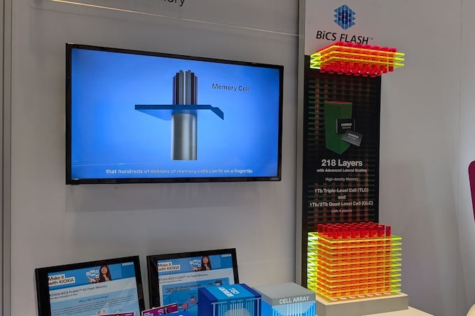
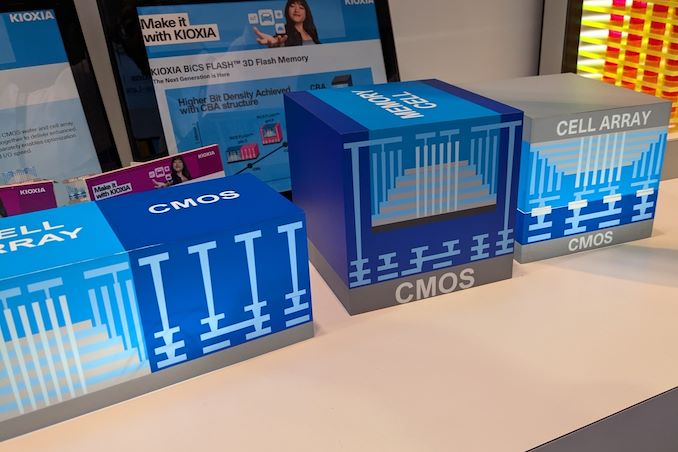
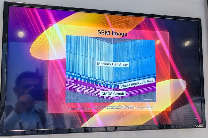
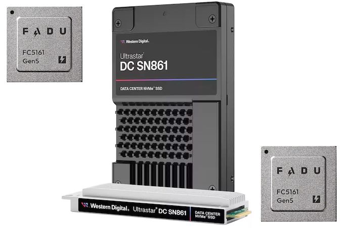
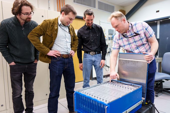
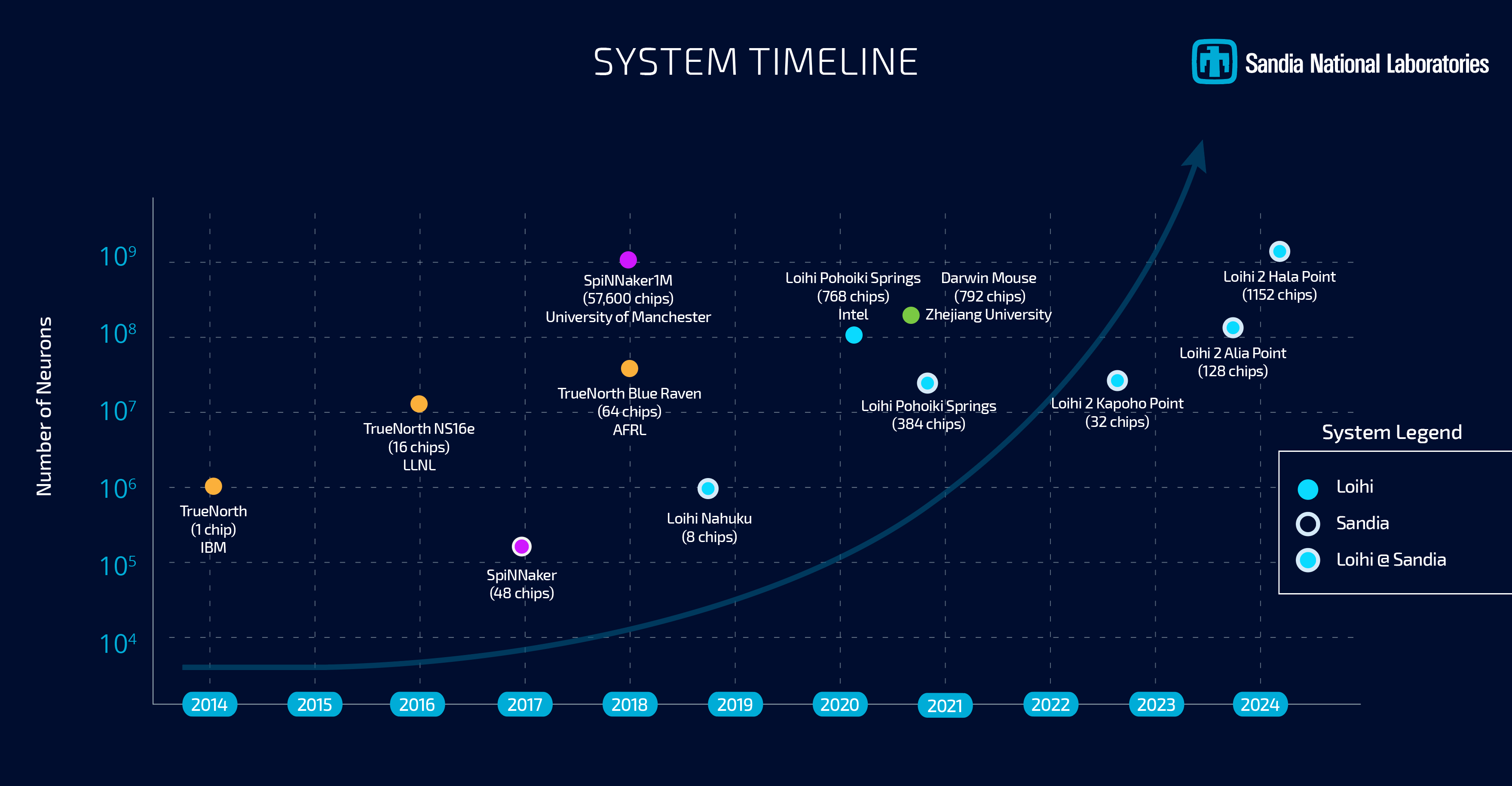
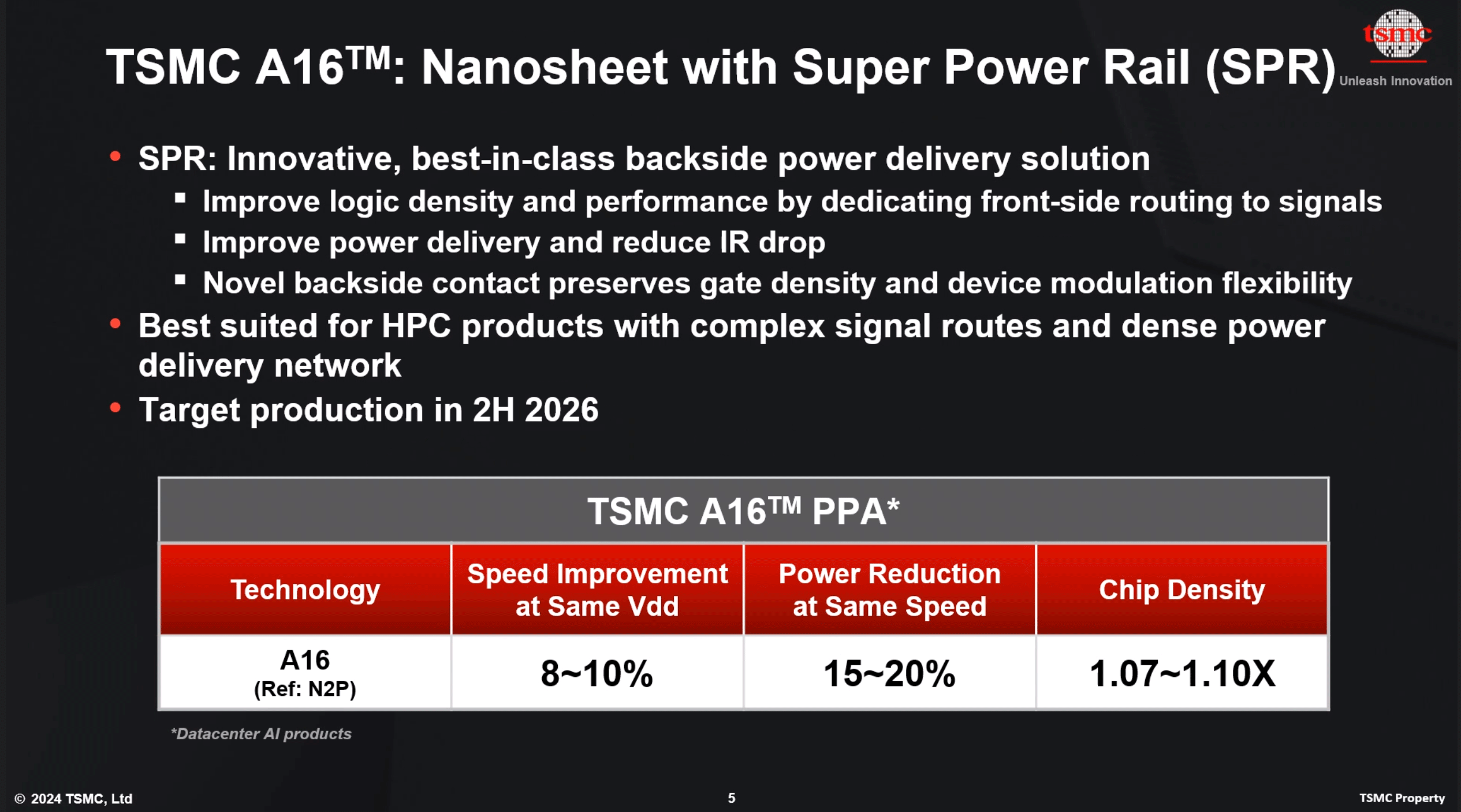
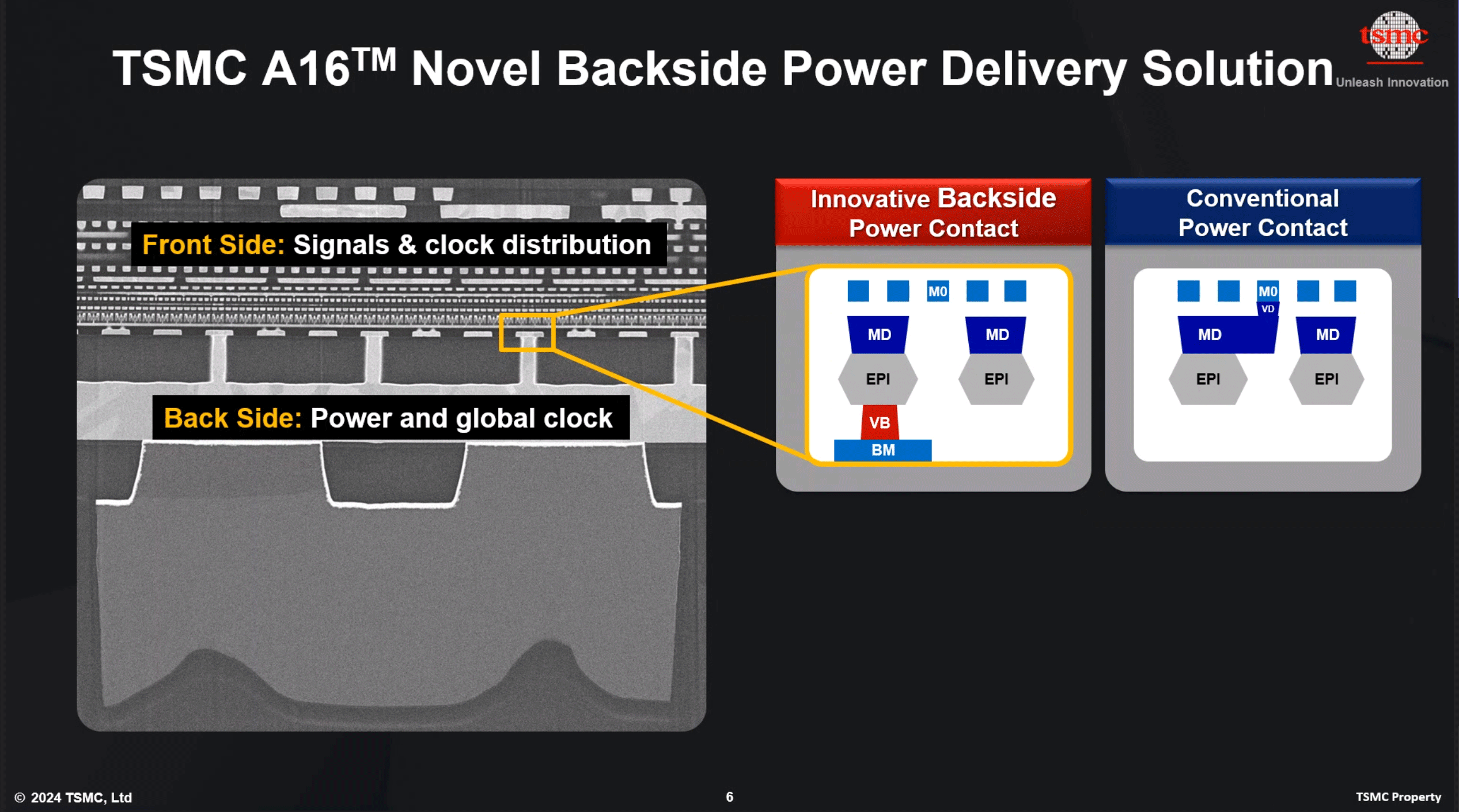
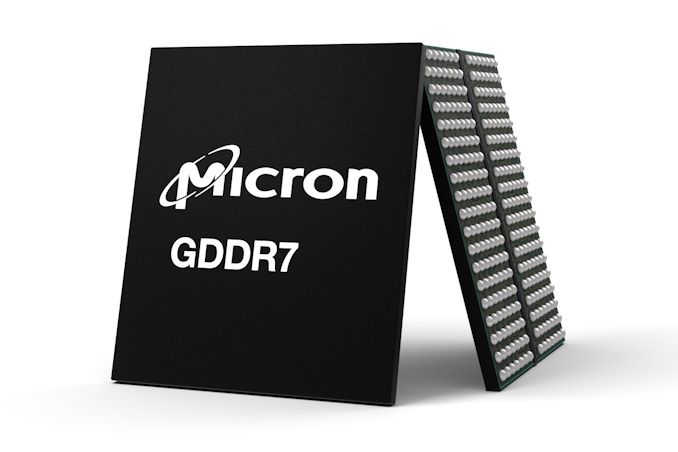
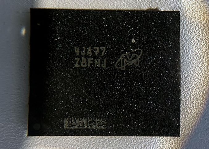
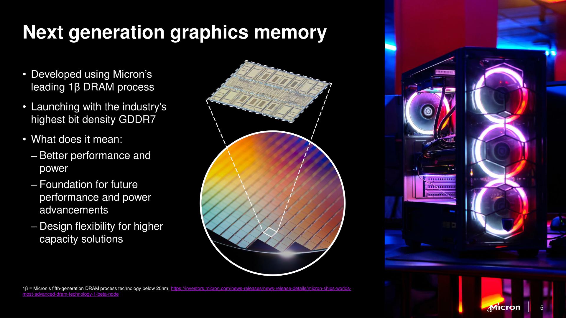
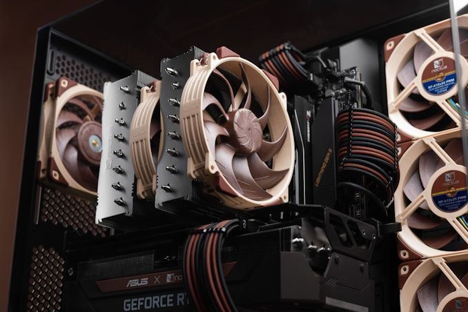
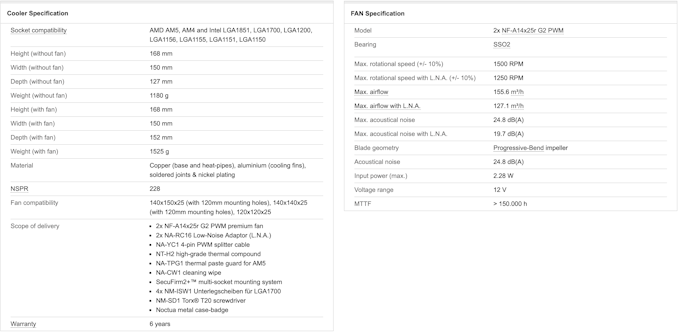
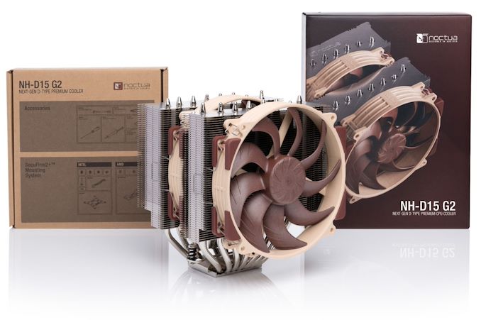
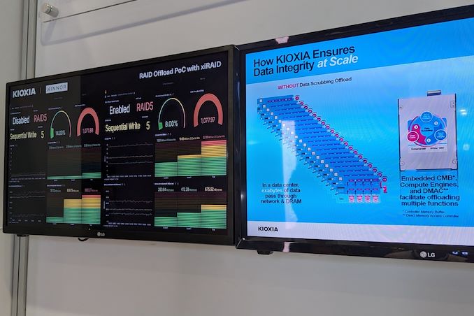
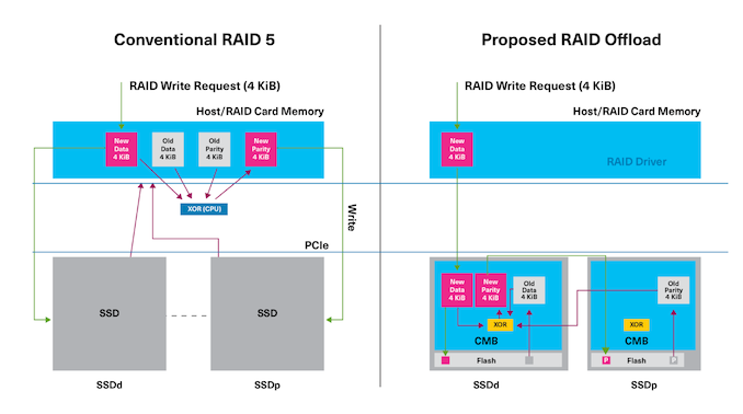

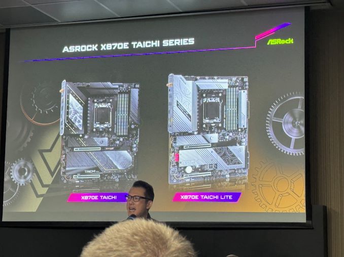
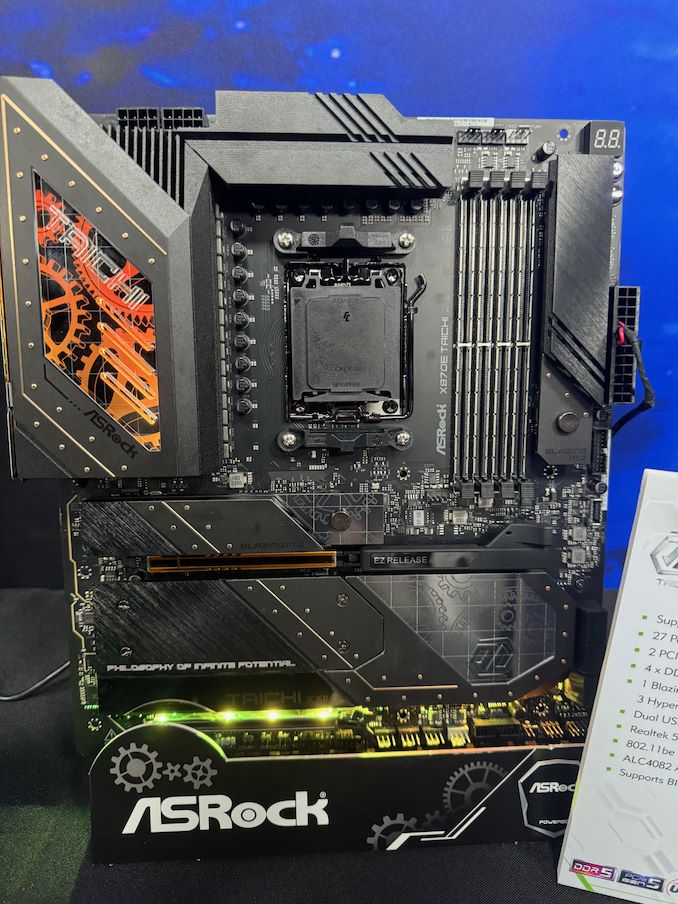
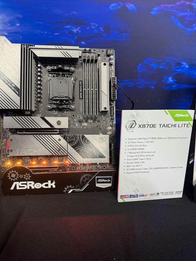

0 Comments