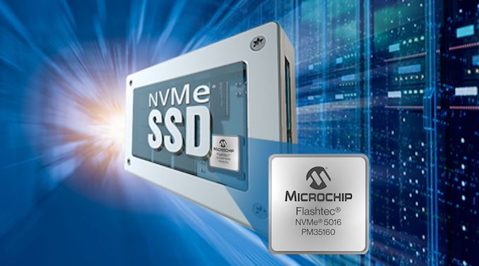

Microchip recently announced the availability of their second PCIe Gen 5 enterprise SSD controller - the Flashtec 5016. Like the 4016, this is also a 16-channel controller, but there are some key updates:
Microchip's enterprise SSD controllers provide a high level of flexibility to SSD vendors by providing them with significant horsepower and accelerators. The 5016 includes Cortex-A53 cores for SSD vendors to run custom applications relevant to SSD management. However, compared to the Gen4 controllers, there are two additional cores in the CPU cluster. The DRAM subsystem includes ECC support (both out-of-band and inline, as desired by the SSD vendor).
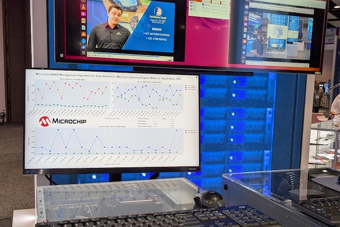
At FMS 2024, the company demonstrated an application of the neural network engines embedded in the Gen5 controllers. Controllers usually employ a 'read-retry' operation with altered read-out voltages for flash reads that do not complete successfully. Microchip implemented a machine learning approach to determine the read-out voltage based on the health history of the NAND block using the NN engines in the controller. This approach delivers tangible benefits for read latency and power consumption (thanks to a smaller number of errors on the first read).
The 4016 and 5016 come with a single-chip root of trust implementation for hardware security. A secure boot process with dual-signature authentication ensures that the controller firmware is not maliciously altered in the field. The company also brought out the advantages of their controller's implementation of SR-IOV, flexible data placement, and zoned namespaces along with their 'credit engine' scheme for multi-tenant cloud workloads. These aspects were also brought out in other demonstrations.
Microchip's press release included quotes from the usual NAND vendors - Solidigm, Kioxia, and Micron. On the customer front, Longsys has been using Flashtec controllers in their enterprise offerings along with YMTC NAND. It is likely that this collaboration will continue further using the new 5016 controller.
Storage

As Seagate ramps up shipments of its new heat assisted magnetic recording (HAMR)-based Mozaic 3+ hard drive platform, the company is both in the enviable position of shipping the first major new hard drive technology in a decade, and the much less enviable position of proving the reliability of the first major new hard drive technology in a decade. Due to HAMR's use of temporal heating with its platters, as well as all-new read/write heads, HAMR introduces multiple new changes at once that have raise questions about how reliable the technology will be. Looking to address these matters (and further promote their HAMR drives), Seagate has published a fresh blog post outlining the company's R&D efforts, and why the company expects their HAMR drives to last several years – as long or longer than current PMR hard drives.
According to the company, the reliability of Mozaic 3+ drives on par with traditional drives relying on perpendicular magnetic recording (PMR), the company says. In fact, components of HAMR HDDs have demonstrated a 50% increase in reliability over the past two years. Seagate says that Mozaic 3+ drives boast impressive durability metrics: their read/write heads have demonstrated capacity to handle over 3.2 petabytes of data transfer over 6,000 hours of operation, which exceeds data transfers of typical nearline hard drives by 20 times. Accordingly, Seagate is rating these drives for a mean time between failure (MTBF) 2.5 million hours, which is in-line with PMR-based drives.
Based on their field stress tests, involving over 500,000 Mozaic 3+ drives, Seagate says that the heads of Mozaic 3+ drives will last over seven years, surpassing the typical lifespan of current PMR-based drives. Generally, customers anticipate that modern PMR drives will last between four and five years with average usage, so these drives would exceed current expectations.
Altogether, Seagate is continuing aim for a seamless transition from PMR to HAMR drives in customer systems. That means ensuring that these new drives can fit into existing data center infrastructures without requiring any changes to enterprise specifications, warranty conditions, or form factors.
Storage
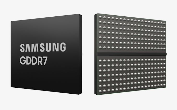
Now that JEDEC has published specification of GDDR7 memory, memory manufacturers are beginning to announce their initial products. The first out of the gate for this generation is Samsung, which has has quietly added its GDDR7 products to its official product catalog.
For now, Samsung lists two GDDR7 devices on its website: 16 Gbit chips rated for an up to 28 GT/s data transfer rate and a faster version running at up to 32 GT/s data transfer rate (which is in line with initial parts that Samsung announced in mid-2023). The chips feature a 512M x32 organization and come in a 266-pin FBGA packaging. The chips are already sampling, so Samsung's customers – GPU vendors, AI inference vendors, network product vendors, and the like – should already have GDDR7 chips in their labs.
The GDDR7 specification promises the maximum per-chip capacity of 64 Gbit (8 GB) and data transfer rates of 48 GT/s. Meanwhile, first generation GDDR7 chips (as announced so far) will feature a rather moderate capacity of 16 Gbit (2 GB) and a data transfer rate of up to 32 GT/s.
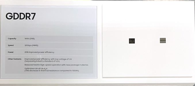
Performance-wise, the first generation of GDDR7 should provide a significant improvement in memory bandwidth over GDDR6 and GDDR6X. However capacity/density improvements will not come until memory manufacturers move to their next generation EUV-based process nodes. As a result, the first GDDR7-based graphics cards are unlikely to sport any memory capacity improvements. Though looking a bit farther down the road, Samsung and SK Hynix have previously told Tom's Hardware that they intend to reach mass production of 24 Gbit GDDR7 chips in 2025.
Otherwise, it is noteworthy that SK Hynix also demonstrated its GDDR7 chips at NVIDIA's GTC last week. So Samsung's competition should be close behind in delivering samples, and eventually mass production memory.
Source: Samsung (via @harukaze5719)
Memory
The CXL consortium has had a regular presence at FMS (which rechristened itself from 'Flash Memory Summit' to the 'Future of Memory and Storage' this year). Back at FMS 2022, the company had announced v3.0 of the CXL specifications. This was followed by CXL 3.1's introduction at Supercomputing 2023. Having started off as a host to device interconnect standard, it had slowly subsumed other competing standards such as OpenCAPI and Gen-Z. As a result, the specifications started to encompass a wide variety of use-cases by building a protocol on top of the the ubiquitous PCIe expansion bus. The CXL consortium comprises of heavyweights such as AMD and Intel, as well as a large number of startup companies attempting to play in different segments on the device side. At FMS 2024, CXL had a prime position in the booth demos of many vendors.
The migration of server platforms from DDR4 to DDR5, along with the rise of workloads demanding large RAM capacity (but not particularly sensitive to either memory bandwidth or latency), has opened up memory expansion modules as one of the first set of widely available CXL devices. Over the last couple of years, we have had product announcements from Samsung and Micron in this area.
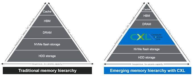
At FMS 2024, SK hynix was showing off their DDR5-based CMM-DDR5 CXL memory module with a 128 GB capacity. The company was also detailing their associated Heterogeneous Memory Software Development Kit (HMSDK) - a set of libraries and tools at both the kernel and user levels aimed at increasing the ease of use of CXL memory. This is achieved in part by considering the memory pyramid / hierarchy and relocating the data between the server's main memory (DRAM) and the CXL device based on usage frequency.
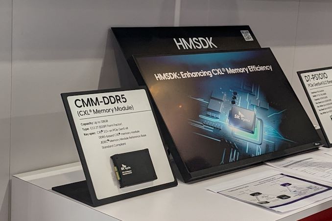
The CMM-DDR5 CXL memory module comes in the SDFF form-factor (E3.S 2T) with a PCIe 3.0 x8 host interface. The internal memory is based on 1α technology DRAM, and the device promises DDR5-class bandwidth and latency within a single NUMA hop. As these memory modules are meant to be used in datacenters and enterprises, the firmware includes features for RAS (reliability, availability, and serviceability) along with secure boot and other management features.
SK hynix was also demonstrating Niagara 2.0 - a hardware solution (currently based on FPGAs) to enable memory pooling and sharing - i.e, connecting multiple CXL memories to allow different hosts (CPUs and GPUs) to optimally share their capacity. The previous version only allowed capacity sharing, but the latest version enables sharing of data also. SK hynix had presented these solutions at the CXL DevCon 2024 earlier this year, but some progress seems to have been made in finalizing the specifications of the CMM-DDR5 at FMS 2024.
Micron had unveiled the CZ120 CXL Memory Expansion Module last year based on the Microchip SMC 2000 series CXL memory controller. At FMS 2024, Micron and Microchip had a demonstration of the module on a Granite Rapids server.
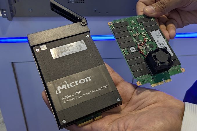
Additional insights into the SMC 2000 controller were also provided.
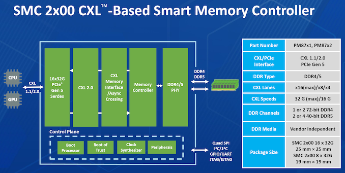
The CXL memory controller also incorporates DRAM die failure handling, and Microchip also provides diagnostics and debug tools to analyze failed modules. The memory controller also supports ECC, which forms part of the enterprise... Storage
As Seagate ramps up shipments of its new heat assisted magnetic recording (HAMR)-based Mozaic 3+ hard drive platform, the company is both in the enviable position of shipping the first major new hard drive technology in a decade, and the much less enviable position of proving the reliability of the first major new hard drive technology in a decade. Due to HAMR's use of temporal heating with its platters, as well as all-new read/write heads, HAMR introduces multiple new changes at once that have raise questions about how reliable the technology will be. Looking to address these matters (and further promote their HAMR drives), Seagate has published a fresh blog post outlining the company's R&D efforts, and why the company expects their HAMR drives to last several years – as long or longer than current PMR hard drives.
According to the company, the reliability of Mozaic 3+ drives on par with traditional drives relying on perpendicular magnetic recording (PMR), the company says. In fact, components of HAMR HDDs have demonstrated a 50% increase in reliability over the past two years. Seagate says that Mozaic 3+ drives boast impressive durability metrics: their read/write heads have demonstrated capacity to handle over 3.2 petabytes of data transfer over 6,000 hours of operation, which exceeds data transfers of typical nearline hard drives by 20 times. Accordingly, Seagate is rating these drives for a mean time between failure (MTBF) 2.5 million hours, which is in-line with PMR-based drives.
Based on their field stress tests, involving over 500,000 Mozaic 3+ drives, Seagate says that the heads of Mozaic 3+ drives will last over seven years, surpassing the typical lifespan of current PMR-based drives. Generally, customers anticipate that modern PMR drives will last between four and five years with average usage, so these drives would exceed current expectations.
Altogether, Seagate is continuing aim for a seamless transition from PMR to HAMR drives in customer systems. That means ensuring that these new drives can fit into existing data center infrastructures without requiring any changes to enterprise specifications, warranty conditions, or form factors.
Storage
Now that JEDEC has published specification of GDDR7 memory, memory manufacturers are beginning to announce their initial products. The first out of the gate for this generation is Samsung, which has has quietly added its GDDR7 products to its official product catalog.
For now, Samsung lists two GDDR7 devices on its website: 16 Gbit chips rated for an up to 28 GT/s data transfer rate and a faster version running at up to 32 GT/s data transfer rate (which is in line with initial parts that Samsung announced in mid-2023). The chips feature a 512M x32 organization and come in a 266-pin FBGA packaging. The chips are already sampling, so Samsung's customers – GPU vendors, AI inference vendors, network product vendors, and the like – should already have GDDR7 chips in their labs.
The GDDR7 specification promises the maximum per-chip capacity of 64 Gbit (8 GB) and data transfer rates of 48 GT/s. Meanwhile, first generation GDDR7 chips (as announced so far) will feature a rather moderate capacity of 16 Gbit (2 GB) and a data transfer rate of up to 32 GT/s.
Performance-wise, the first generation of GDDR7 should provide a significant improvement in memory bandwidth over GDDR6 and GDDR6X. However capacity/density improvements will not come until memory manufacturers move to their next generation EUV-based process nodes. As a result, the first GDDR7-based graphics cards are unlikely to sport any memory capacity improvements. Though looking a bit farther down the road, Samsung and SK Hynix have previously told Tom's Hardware that they intend to reach mass production of 24 Gbit GDDR7 chips in 2025.
Otherwise, it is noteworthy that SK Hynix also demonstrated its GDDR7 chips at NVIDIA's GTC last week. So Samsung's competition should be close behind in delivering samples, and eventually mass production memory.
Source: Samsung (via @harukaze5719)
Memory
The CXL consortium has had a regular presence at FMS (which rechristened itself from 'Flash Memory Summit' to the 'Future of Memory and Storage' this year). Back at FMS 2022, the company had announced v3.0 of the CXL specifications. This was followed by CXL 3.1's introduction at Supercomputing 2023. Having started off as a host to device interconnect standard, it had slowly subsumed other competing standards such as OpenCAPI and Gen-Z. As a result, the specifications started to encompass a wide variety of use-cases by building a protocol on top of the the ubiquitous PCIe expansion bus. The CXL consortium comprises of heavyweights such as AMD and Intel, as well as a large number of startup companies attempting to play in different segments on the device side. At FMS 2024, CXL had a prime position in the booth demos of many vendors.
The migration of server platforms from DDR4 to DDR5, along with the rise of workloads demanding large RAM capacity (but not particularly sensitive to either memory bandwidth or latency), has opened up memory expansion modules as one of the first set of widely available CXL devices. Over the last couple of years, we have had product announcements from Samsung and Micron in this area.
At FMS 2024, SK hynix was showing off their DDR5-based CMM-DDR5 CXL memory module with a 128 GB capacity. The company was also detailing their associated Heterogeneous Memory Software Development Kit (HMSDK) - a set of libraries and tools at both the kernel and user levels aimed at increasing the ease of use of CXL memory. This is achieved in part by considering the memory pyramid / hierarchy and relocating the data between the server's main memory (DRAM) and the CXL device based on usage frequency.
The CMM-DDR5 CXL memory module comes in the SDFF form-factor (E3.S 2T) with a PCIe 3.0 x8 host interface. The internal memory is based on 1α technology DRAM, and the device promises DDR5-class bandwidth and latency within a single NUMA hop. As these memory modules are meant to be used in datacenters and enterprises, the firmware includes features for RAS (reliability, availability, and serviceability) along with secure boot and other management features.
SK hynix was also demonstrating Niagara 2.0 - a hardware solution (currently based on FPGAs) to enable memory pooling and sharing - i.e, connecting multiple CXL memories to allow different hosts (CPUs and GPUs) to optimally share their capacity. The previous version only allowed capacity sharing, but the latest version enables sharing of data also. SK hynix had presented these solutions at the CXL DevCon 2024 earlier this year, but some progress seems to have been made in finalizing the specifications of the CMM-DDR5 at FMS 2024.
Micron had unveiled the CZ120 CXL Memory Expansion Module last year based on the Microchip SMC 2000 series CXL memory controller. At FMS 2024, Micron and Microchip had a demonstration of the module on a Granite Rapids server.
Additional insights into the SMC 2000 controller were also provided.
The CXL memory controller also incorporates DRAM die failure handling, and Microchip also provides diagnostics and debug tools to analyze failed modules. The memory controller also supports ECC, which forms part of the enterprise... Storage
The CXL consortium has had a regular presence at FMS (which rechristened itself from 'Flash Memory Summit' to the 'Future of Memory and Storage' this year). Back at FMS 2022, the company had announced v3.0 of the CXL specifications. This was followed by CXL 3.1's introduction at Supercomputing 2023. Having started off as a host to device interconnect standard, it had slowly subsumed other competing standards such as OpenCAPI and Gen-Z. As a result, the specifications started to encompass a wide variety of use-cases by building a protocol on top of the the ubiquitous PCIe expansion bus. The CXL consortium comprises of heavyweights such as AMD and Intel, as well as a large number of startup companies attempting to play in different segments on the device side. At FMS 2024, CXL had a prime position in the booth demos of many vendors.
The migration of server platforms from DDR4 to DDR5, along with the rise of workloads demanding large RAM capacity (but not particularly sensitive to either memory bandwidth or latency), has opened up memory expansion modules as one of the first set of widely available CXL devices. Over the last couple of years, we have had product announcements from Samsung and Micron in this area.
At FMS 2024, SK hynix was showing off their DDR5-based CMM-DDR5 CXL memory module with a 128 GB capacity. The company was also detailing their associated Heterogeneous Memory Software Development Kit (HMSDK) - a set of libraries and tools at both the kernel and user levels aimed at increasing the ease of use of CXL memory. This is achieved in part by considering the memory pyramid / hierarchy and relocating the data between the server's main memory (DRAM) and the CXL device based on usage frequency.
The CMM-DDR5 CXL memory module comes in the SDFF form-factor (E3.S 2T) with a PCIe 3.0 x8 host interface. The internal memory is based on 1α technology DRAM, and the device promises DDR5-class bandwidth and latency within a single NUMA hop. As these memory modules are meant to be used in datacenters and enterprises, the firmware includes features for RAS (reliability, availability, and serviceability) along with secure boot and other management features.
SK hynix was also demonstrating Niagara 2.0 - a hardware solution (currently based on FPGAs) to enable memory pooling and sharing - i.e, connecting multiple CXL memories to allow different hosts (CPUs and GPUs) to optimally share their capacity. The previous version only allowed capacity sharing, but the latest version enables sharing of data also. SK hynix had presented these solutions at the CXL DevCon 2024 earlier this year, but some progress seems to have been made in finalizing the specifications of the CMM-DDR5 at FMS 2024.
Micron had unveiled the CZ120 CXL Memory Expansion Module last year based on the Microchip SMC 2000 series CXL memory controller. At FMS 2024, Micron and Microchip had a demonstration of the module on a Granite Rapids server.
Additional insights into the SMC 2000 controller were also provided.
The CXL memory controller also incorporates DRAM die failure handling, and Microchip also provides diagnostics and debug tools to analyze failed modules. The memory controller also supports ECC, which forms part of the enterprise... Storage

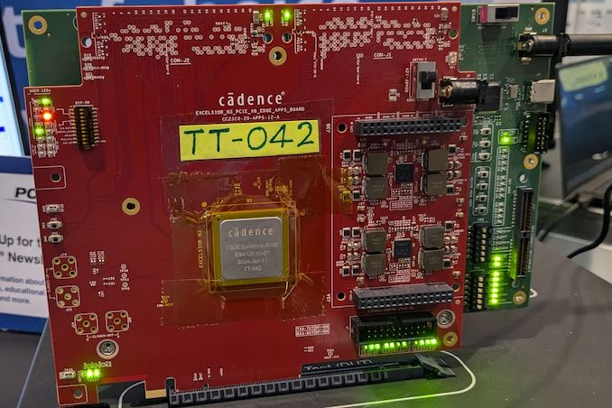
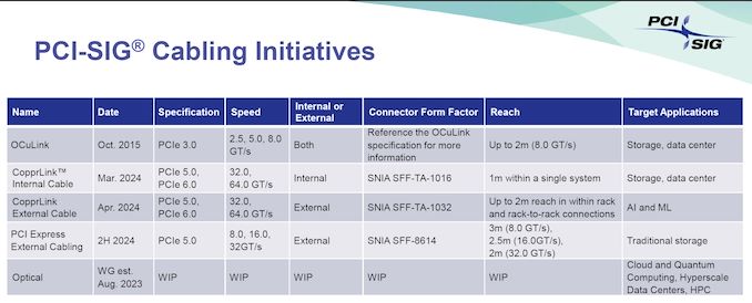
PCI-SIG this week released version 0.5 of the PCI-Express 7.0 specification to its members. This is the second draft of the spec and the final call for PCI-SIG members to submit their new features to the standard. The latest update on the development of the specification comes a couple months shy of a year after the PCI-SIG published the initial Draft 0.3 specificaiton, with the PCI-SIG using the latest update to reiterate that development of the new standard remains on-track for a final release in 2025.
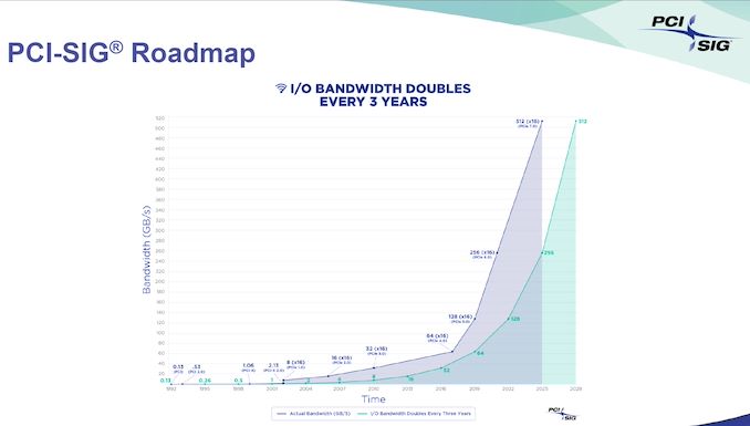
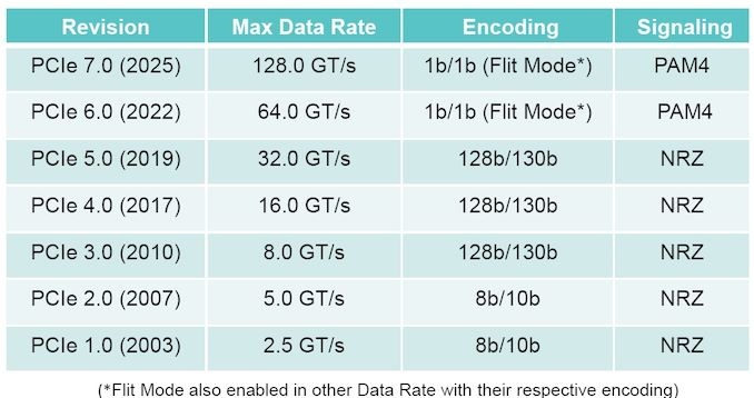
PCIe 7.0 is is the next generation interconnect technology for computers that is set to increase data transfer speeds to 128 GT/s per pin, doubling the 64 GT/s of PCIe 6.0 and quadrupling the 32 GT/s of PCIe 5.0. This would allow a 16-lane (x16) connection to support 256 GB/sec of bandwidth in each direction simultaneously, excluding encoding overhead. Such speeds will be handy for future datacenters as well as artificial intelligence and high-performance computing applications that will need even faster data transfer rates, including network data transfer rates.
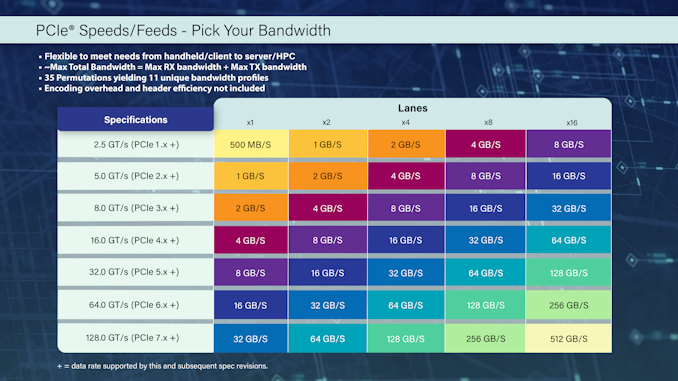
To achieve its impressive data transfer rates, PCIe 7.0 doubles the bus frequency at the physical layer compared to PCIe 5.0 and 6.0. Otherwise, the standard retains pulse amplitude modulation with four level signaling (PAM4), 1b/1b FLIT mode encoding, and the forward error correction (FEC) technologies that are already used for PCIe 6.0. Otherwise, PCI-SIG says that the PCIe 7.0 speicification also focuses on enhanced channel parameters and reach as well as improved power efficiency.
Overall, the engineers behind the standard have their work cut out for them, given that PCIe 7.0 requires doubling the bus frequency at the physical layer, a major development that PCIe 6.0 sidestepped with PAM4 signaling. Nothing comes for free in regards to improving data signaling, and with PCIe 7.0, the PCI-SIG is arguably back to hard-mode development by needing to improve the physical layer once more – this time to enable it to run at around 30GHz. Though how much of this heavy lifting will be accomplished through smart signaling (and retimers) and how much will be accomplished through sheer materials improvements, such as thicker printed circuit boards (PCBs) and low-loss materials, remains to be seen.
The next major step for PCIe 7.0 is finalization of the version 0.7 of specification, which is considered the Complete Draft, where all aspects must be fully defined, and electrical specifications must be validated through test chips. After this iteration of the specification is released, no new features can be added. PCIe 6.0 eventually went through 4 major drafts – 0.3, 0.5, 0.7, and 0.9 – before finally being finalized, so PCIe 7.0 is likely on the same track.
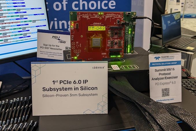
Once finalized in 2025, it should take a few years for the first PCIe 7.0 hardware to hit the shelves. Although development work on controller IP and initial hardware is already underway, that process extends well beyond the release of the final PCIe specification.
CPUs
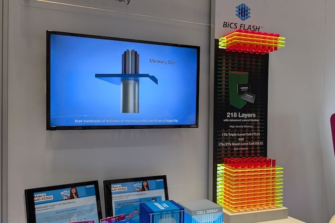
Kioxia's booth at FMS 2024 was a busy one with multiple technology demonstrations keeping visitors occupied. A walk-through of the BiCS 8 manufacturing process was the first to grab my attention. Kioxia and Western Digital announced the sampling of BiCS 8 in March 2023. We had touched briefly upon its CMOS Bonded Array (CBA) scheme in our coverage of Kioxial's 2Tb QLC NAND device and coverage of Western Digital's 128 TB QLC enterprise SSD proof-of-concept demonstration. At Kioxia's booth, we got more insights.
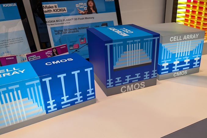
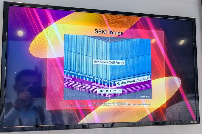
Traditionally, fabrication of flash chips involved placement of the associate logic circuitry (CMOS process) around the periphery of the flash array. The process then moved on to putting the CMOS under the cell array, but the wafer development process was serialized with the CMOS logic getting fabricated first followed by the cell array on top. However, this has some challenges because the cell array requires a high-temperature processing step to ensure higher reliability that can be detrimental to the health of the CMOS logic. Thanks to recent advancements in wafer bonding techniques, the new CBA process allows the CMOS wafer and cell array wafer to be processed independently in parallel and then pieced together, as shown in the models above.
The BiCS 8 3D NAND incorporates 218 layers, compared to 112 layers in BiCS 5 and 162 layers in BiCS 6. The company decided to skip over BiCS 7 (or, rather, it was probably a short-lived generation meant as an internal test vehicle). The generation retains the four-plane charge trap structure of BiCS 6. In its TLC avatar, it is available as a 1 Tbit device. The QLC version is available in two capacities - 1 Tbit and 2 Tbit.
Kioxia also noted that while the number of layers (218) doesn't compare favorably with the latest layer counts from the competition, its lateral scaling / cell shrinkage has enabled it to be competitive in terms of bit density as well as operating speeds (3200 MT/s). For reference, the latest shipping NAND from Micron - the G9 - has 276 layers with a bit density in TLC mode of 21 Gbit/mm2, and operates at up to 3600 MT/s. However, its 232L NAND operates only up to 2400 MT/s and has a bit density of 14.6 Gbit/mm2.
It must be noted that the CBA hybrid bonding process has advantages over the current processes used by other vendors - including Micron's CMOS under array (CuA) and SK hynix's 4D PUC (periphery-under-chip) developed in the late 2010s. It is expected that other NAND vendors will also move eventually to some variant of the hybrid bonding scheme used by Kioxia.
Storage
Kioxia's booth at FMS 2024 was a busy one with multiple technology demonstrations keeping visitors occupied. A walk-through of the BiCS 8 manufacturing process was the first to grab my attention. Kioxia and Western Digital announced the sampling of BiCS 8 in March 2023. We had touched briefly upon its CMOS Bonded Array (CBA) scheme in our coverage of Kioxial's 2Tb QLC NAND device and coverage of Western Digital's 128 TB QLC enterprise SSD proof-of-concept demonstration. At Kioxia's booth, we got more insights.
Traditionally, fabrication of flash chips involved placement of the associate logic circuitry (CMOS process) around the periphery of the flash array. The process then moved on to putting the CMOS under the cell array, but the wafer development process was serialized with the CMOS logic getting fabricated first followed by the cell array on top. However, this has some challenges because the cell array requires a high-temperature processing step to ensure higher reliability that can be detrimental to the health of the CMOS logic. Thanks to recent advancements in wafer bonding techniques, the new CBA process allows the CMOS wafer and cell array wafer to be processed independently in parallel and then pieced together, as shown in the models above.
The BiCS 8 3D NAND incorporates 218 layers, compared to 112 layers in BiCS 5 and 162 layers in BiCS 6. The company decided to skip over BiCS 7 (or, rather, it was probably a short-lived generation meant as an internal test vehicle). The generation retains the four-plane charge trap structure of BiCS 6. In its TLC avatar, it is available as a 1 Tbit device. The QLC version is available in two capacities - 1 Tbit and 2 Tbit.
Kioxia also noted that while the number of layers (218) doesn't compare favorably with the latest layer counts from the competition, its lateral scaling / cell shrinkage has enabled it to be competitive in terms of bit density as well as operating speeds (3200 MT/s). For reference, the latest shipping NAND from Micron - the G9 - has 276 layers with a bit density in TLC mode of 21 Gbit/mm2, and operates at up to 3600 MT/s. However, its 232L NAND operates only up to 2400 MT/s and has a bit density of 14.6 Gbit/mm2.
It must be noted that the CBA hybrid bonding process has advantages over the current processes used by other vendors - including Micron's CMOS under array (CuA) and SK hynix's 4D PUC (periphery-under-chip) developed in the late 2010s. It is expected that other NAND vendors will also move eventually to some variant of the hybrid bonding scheme used by Kioxia.
Storage
Lorem Ipsum is simply dummy text of the printing and typesetting industry. Lorem Ipsum has been the industry's.
As Seagate ramps up shipments of its new heat assisted magnetic recording (HAMR)-based Mozaic 3+ hard drive platform, the company is both in the enviable position of shipping the first major new hard drive technology in a decade, and the much less enviable position of proving the reliability of the first major new hard drive technology in a decade. Due to HAMR's use of temporal heating with its platters, as well as all-new read/write heads, HAMR introduces multiple new changes at once that have raise questions about how reliable the technology will be. Looking to address these matters (and further promote their HAMR drives), Seagate has published a fresh blog post outlining the company's R&D efforts, and why the company expects their HAMR drives to last several years – as long or longer than current PMR hard drives.
According to the company, the reliability of Mozaic 3+ drives on par with traditional drives relying on perpendicular magnetic recording (PMR), the company says. In fact, components of HAMR HDDs have demonstrated a 50% increase in reliability over the past two years. Seagate says that Mozaic 3+ drives boast impressive durability metrics: their read/write heads have demonstrated capacity to handle over 3.2 petabytes of data transfer over 6,000 hours of operation, which exceeds data transfers of typical nearline hard drives by 20 times. Accordingly, Seagate is rating these drives for a mean time between failure (MTBF) 2.5 million hours, which is in-line with PMR-based drives.
Based on their field stress tests, involving over 500,000 Mozaic 3+ drives, Seagate says that the heads of Mozaic 3+ drives will last over seven years, surpassing the typical lifespan of current PMR-based drives. Generally, customers anticipate that modern PMR drives will last between four and five years with average usage, so these drives would exceed current expectations.
Altogether, Seagate is continuing aim for a seamless transition from PMR to HAMR drives in customer systems. That means ensuring that these new drives can fit into existing data center infrastructures without requiring any changes to enterprise specifications, warranty conditions, or form factors.
Storage
Now that JEDEC has published specification of GDDR7 memory, memory manufacturers are beginning to announce their initial products. The first out of the gate for this generation is Samsung, which has has quietly added its GDDR7 products to its official product catalog.
For now, Samsung lists two GDDR7 devices on its website: 16 Gbit chips rated for an up to 28 GT/s data transfer rate and a faster version running at up to 32 GT/s data transfer rate (which is in line with initial parts that Samsung announced in mid-2023). The chips feature a 512M x32 organization and come in a 266-pin FBGA packaging. The chips are already sampling, so Samsung's customers – GPU vendors, AI inference vendors, network product vendors, and the like – should already have GDDR7 chips in their labs.
The GDDR7 specification promises the maximum per-chip capacity of 64 Gbit (8 GB) and data transfer rates of 48 GT/s. Meanwhile, first generation GDDR7 chips (as announced so far) will feature a rather moderate capacity of 16 Gbit (2 GB) and a data transfer rate of up to 32 GT/s.
Performance-wise, the first generation of GDDR7 should provide a significant improvement in memory bandwidth over GDDR6 and GDDR6X. However capacity/density improvements will not come until memory manufacturers move to their next generation EUV-based process nodes. As a result, the first GDDR7-based graphics cards are unlikely to sport any memory capacity improvements. Though looking a bit farther down the road, Samsung and SK Hynix have previously told Tom's Hardware that they intend to reach mass production of 24 Gbit GDDR7 chips in 2025.
Otherwise, it is noteworthy that SK Hynix also demonstrated its GDDR7 chips at NVIDIA's GTC last week. So Samsung's competition should be close behind in delivering samples, and eventually mass production memory.
Source: Samsung (via @harukaze5719)
Memory



.</p>
<p align="center"><a href="https://www.anandtech.com/show/21514/microship-demonstrates-flashtec-5016-enterprise-ssd-controller"><img alt="" src="https://images.anandtech.com/doci/21514/flashtec-ml_575px.jpg" /></a></p>
<p>At FMS 2024, the company demonstrated an application of the neural network engines embedded in the Gen5 controllers. Controllers usually employ a 'read-retry' operation with altered read-out voltages for flash reads that do not complete successfully. Microchip implemented a machine learning approach to determine the read-out voltage based on the health history of the NAND block using the NN engines in the controller. This approach delivers tangible benefits for read latency and power consumption (thanks to a smaller number of errors on the first read).</p>
<p>The 4016 and 5016 come with a single-chip root of trust implementation for hardware security. A secure boot process with dual-signature authentication ensures that the controller firmware is not maliciously altered in the field. The company also brought out the advantages of their controller's implementation of SR-IOV, flexible data placement, and zoned namespaces along with their 'credit engine' scheme for multi-tenant cloud workloads. These aspects were also brought out in other demonstrations.</p>
<p>Microchip's press release included quotes from the usual NAND vendors - Solidigm, Kioxia, and Micron. On the customer front, Longsys has been using Flashtec controllers in their enterprise offerings along with YMTC NAND. It is likely that this collaboration will continue further using the new 5016 controller.</p>
</p> Storage)
.</p>
<p align="center"><a href="https://www.anandtech.com/show/21514/microship-demonstrates-flashtec-5016-enterprise-ssd-controller"><img alt="" src="https://images.anandtech.com/doci/21514/flashtec-ml_575px.jpg" /></a></p>
<p>At FMS 2024, the company demonstrated an application of the neural network engines embedded in the Gen5 controllers. Controllers usually employ a 'read-retry' operation with altered read-out voltages for flash reads that do not complete successfully. Microchip implemented a machine learning approach to determine the read-out voltage based on the health history of the NAND block using the NN engines in the controller. This approach delivers tangible benefits for read latency and power consumption (thanks to a smaller number of errors on the first read).</p>
<p>The 4016 and 5016 come with a single-chip root of trust implementation for hardware security. A secure boot process with dual-signature authentication ensures that the controller firmware is not maliciously altered in the field. The company also brought out the advantages of their controller's implementation of SR-IOV, flexible data placement, and zoned namespaces along with their 'credit engine' scheme for multi-tenant cloud workloads. These aspects were also brought out in other demonstrations.</p>
<p>Microchip's press release included quotes from the usual NAND vendors - Solidigm, Kioxia, and Micron. On the customer front, Longsys has been using Flashtec controllers in their enterprise offerings along with YMTC NAND. It is likely that this collaboration will continue further using the new 5016 controller.</p>
</p> Storage)
.</p>
<p align="center"><a href="https://www.anandtech.com/show/21514/microship-demonstrates-flashtec-5016-enterprise-ssd-controller"><img alt="" src="https://images.anandtech.com/doci/21514/flashtec-ml_575px.jpg" /></a></p>
<p>At FMS 2024, the company demonstrated an application of the neural network engines embedded in the Gen5 controllers. Controllers usually employ a 'read-retry' operation with altered read-out voltages for flash reads that do not complete successfully. Microchip implemented a machine learning approach to determine the read-out voltage based on the health history of the NAND block using the NN engines in the controller. This approach delivers tangible benefits for read latency and power consumption (thanks to a smaller number of errors on the first read).</p>
<p>The 4016 and 5016 come with a single-chip root of trust implementation for hardware security. A secure boot process with dual-signature authentication ensures that the controller firmware is not maliciously altered in the field. The company also brought out the advantages of their controller's implementation of SR-IOV, flexible data placement, and zoned namespaces along with their 'credit engine' scheme for multi-tenant cloud workloads. These aspects were also brought out in other demonstrations.</p>
<p>Microchip's press release included quotes from the usual NAND vendors - Solidigm, Kioxia, and Micron. On the customer front, Longsys has been using Flashtec controllers in their enterprise offerings along with YMTC NAND. It is likely that this collaboration will continue further using the new 5016 controller.</p>
</p> Storage | https://compbuddey.blogspot.com/2025/02/microchip-demonstrates-flashtec-5016_9.html)
.</p>
<p align="center"><a href="https://www.anandtech.com/show/21514/microship-demonstrates-flashtec-5016-enterprise-ssd-controller"><img alt="" src="https://images.anandtech.com/doci/21514/flashtec-ml_575px.jpg" /></a></p>
<p>At FMS 2024, the company demonstrated an application of the neural network engines embedded in the Gen5 controllers. Controllers usually employ a 'read-retry' operation with altered read-out voltages for flash reads that do not complete successfully. Microchip implemented a machine learning approach to determine the read-out voltage based on the health history of the NAND block using the NN engines in the controller. This approach delivers tangible benefits for read latency and power consumption (thanks to a smaller number of errors on the first read).</p>
<p>The 4016 and 5016 come with a single-chip root of trust implementation for hardware security. A secure boot process with dual-signature authentication ensures that the controller firmware is not maliciously altered in the field. The company also brought out the advantages of their controller's implementation of SR-IOV, flexible data placement, and zoned namespaces along with their 'credit engine' scheme for multi-tenant cloud workloads. These aspects were also brought out in other demonstrations.</p>
<p>Microchip's press release included quotes from the usual NAND vendors - Solidigm, Kioxia, and Micron. On the customer front, Longsys has been using Flashtec controllers in their enterprise offerings along with YMTC NAND. It is likely that this collaboration will continue further using the new 5016 controller.</p>
</p> Storage&body=https://compbuddey.blogspot.com/2025/02/microchip-demonstrates-flashtec-5016_9.html)


0 Comments