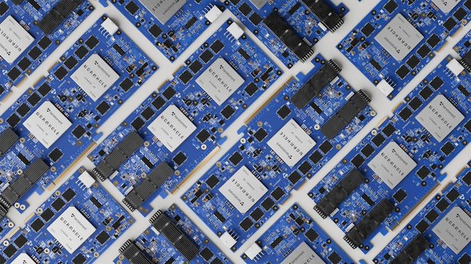

Tenstorrent has unveiled its next-generation Wormhole processor for AI workloads that promises to offer decent performance at a low price. The company currently offers two add-on PCIe cards carrying one or two Wormhole processors as well as TT-LoudBox, and TT-QuietBox workstations aimed at software developers. The whole of today's release is aimed at developers rather than those who will deploy the Wormhole boards for their commercial workloads.
“It is always rewarding to get more of our products into developer hands. Releasing development systems with our Wormhole™ card helps developers scale up and work on multi-chip AI software.” said Jim Keller, CEO of Tenstorrent. “In addition to this launch, we are excited that the tape-out and power-on for our second generation, Blackhole, is going very well.”
Each Wormhole processor packs 72 Tensix cores (featuring five RISC-V cores supporting various data formats) with 108 MB of SRAM to deliver 262 FP8 TFLOPS at 1 GHz at 160W thermal design power. A single-chip Wormhole n150 card carries 12 GB of GDDR6 memory featuring a 288 GB/s bandwidth.
Wormhole processors offer flexible scalability to meet the varying needs of workloads. In a standard workstation setup with four Wormhole n300 cards, the processors can merge to function as a single unit, appearing as a unified, extensive network of Tensix cores to the software. This configuration allows the accelerators to either work on the same workload, be divided among four developers or run up to eight distinct AI models simultaneously. A crucial feature of this scalability is that it operates natively without the need for virtualization. In data center environments, Wormhole processors will scale both inside one machine using PCIe or outside of a single machine using Ethernet.
From performance standpoint, Tenstorrent's single-chip Wormhole n150 card (72 Tensix cores at 1 GHz, 108 MB SRAM, 12 GB GDDR6 at 288 GB/s) is capable of 262 FP8 TFLOPS at 160W, whereas the dual-chip Wormhole n300 board (128 Tensix cores at 1 GHz, 192 MB SRAM, aggregated 24 GB GDDR6 at 576 GB/s) can offer up to 466 FP8 TFLOPS at 300W (according to Tom's Hardware).
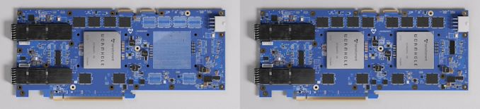
To put that 466 FP8 TFLOPS at 300W number into context, let's compare it to what AI market leader Nvidia has to offer at this thermal design power. Nvidia's A100 does not support FP8, but it does support INT8 and its peak performance is 624 TOPS (1,248 TOPS with sparsity). By contrast, Nvidia's H100 supports FP8 and its peak performance is massive 1,670 TFLOPS (3,341 TFLOPS with sparsity) at 300W, which is a big difference from Tenstorrent's Wormhole n300.
There is a big catch though. Tenstorrent's Wormhole n150 is offered for $999, whereas n300 is available for $1,399. By contrast, one Nvidia H100 card can retail for $30,000, depending on quantities. Of course, we do not know whether four or eight Wormhole processors can indeed deliver the performance of a single H300, though they will do so at 600W or 1200W TDP, respectively.
In addition to cards, Tenstorrent offers developers pre-built workstations with four n300 cards inside the less expensive Xeon-based TT-LoudBox with active cooling and a premium EPYC-powered TT-QuietBox with liquid cooling.
Sources: Tenstorrent, Tom's Hardware
AI

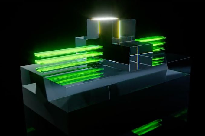
In addition to revealing its roadmap and plans concerning its current leading-edge process technologies, TSMC also shared progress of its N2 node as part of its Symposiums 2024. The company's first 2nm-class fabrication node, and predominantly featuring gate-all-around transistors, according to TSMC N2 has almost achieved its target performance and yield goals, which places it on track to enter high-volume manufacturing in the second half of 2025.
TSMC states that 'N2 development is well on track and N2P is next.' In particular, gate-all-around nanosheet devices currently achieve over 90% of their expected performance, whereas yields of 256 Mb SRAM (32 MB) devices already exceeds 80%, depending on the batch. All of this for a node that is over a year away from mass production.
Meanwhile, average yield of a 256 Mb SRAM was around 70% as of March, 2024, up from around 35% in April, 2023. Device performance has also been improving with higher frequencies being achieved while keeping power consumption in check.
Chip designer interest towards TSMC's first 2nm-class gate-all-around nanosheet transistor-based technology is significant, too. The number of new tape-outs (NTOs) in the first year of N2 is over two-times higher than it was for N5. Though with that said, given TSMC's close working relationship with a handful of high-volume vendors – most notably Appe – NTOs can be a very misleading figure since the first year of a new node at TSMC is capacity constrained, and consequently the bulk of that capacity goes to TSMC's priority partners.
Meanwhile, there were considerably more N5 tapeouts in its second year (some where N5P, of course) and N2 promises to have 2.6X more NTOs in its second year. So the node indeed looks quite promising. In fact, based on TSMC's slides (which we're unfortunately not able to republish), N2 is more popular than N3 in terms of NTOs both in the first and the second years of existence.
When it comes to the second year of N2, in the second half of 2026 TSMC plans to roll out its N2P technology, which promises additional performance and power benefits. N2P is expected to improve frequency by 15% - 20%, reduce power consumption by 30% - 40%, and increase chip density by over 1.15 times compared to N3E, significant benefits to move to all-new GAA nanosheet transistors.
Finally, for those companies that need the best in performance, power, and density, TSMC is poised to offer their A16 process in 2026. That node will also bring in backside power delivery, which will add costs, but is expected to greatly improve performance efficiency and scaling.
Semiconductors
During the opening keynote delivered by AMD CEO Dr. Lisa Su at Computex 2024, AMD finally lifted the lid on their highly-anticipated Zen 5 microarchitecture. The backbone for the next couple of years of everything CPU at AMD, the company unveiled their plans to bring Zen 5 in the consumer market, announcing both their next-generation mobile and desktop products at the same time. With a tight schedule that will see both platforms launch within weeks of each other, today AMD is taking their first step with the launch of the Ryzen AI 300 series – codenamed Strix Point – their new Zen 5-powered mobile SoC.
The latest and greatest from AMD, the Strix Point brings significant architectural improvements across AMD's entire IP portfolio. Headlining the chip, of course, is the company's new Zen 5 CPU microarchitecture, which is taking multiple steps to improve on CPU performance without the benefits of big clockspeed gains. And reflecting the industry's current heavy emphasis on AI performance, Strix Point also includes the latest XDNA 2-based NPU, which boasts up to 50 TOPS of performance. Other improvements include an upgraded integrated graphics processor, with AMD moving to the RDNA 3.5 graphics architecture.
The architectural updates in Strix Point are also seeing AMD opt for a heterogenous CPU design from the very start, incorporating both performance and efficiency cores as a means of offering better overall performance in power-constrained devices. AMD first introduced their compact Zen cores in the middle of the Zen 4 generation, and while they made it into products such as AMD's small-die Phoenix 2 platform, this is the first time AMD's flagship mobile silicon has included them as well. And while this change is going to be transparent from a user perspective, under the hood it represents an important improvement in CPU design. As a result, all Ryzen AI 300 chips are going to include a mix of not only AMD's (mostly) full-fat Zen 5 CPU cores, but also their compact Zen 5c cores, boosting the chips' total CPU core counts and performance in multi-threaded situations.
For today's launch, the AMD Ryzen AI 300 series will consist of just three SKUs: the flagship Ryzen AI 9 HX 375, with 12 CPU cores, as well as the Ryzen AI 9 HX 370 and Ryzen 9 365, with 12 and 10 cores respectively. All three SoCs combine both the regular Zen 5 core with the more compact Zen 5c cores to make up the CPU cluster, and are paired with a powerful Raden 890M/880M GPU, and a XDNA 2-based NPU.
As the successor to the Zen 4-based Phoenix/Hawk Point, the AMD Ryzen AI 300 series is targeting a diverse and active notebook market that has become the largest segment of the PC industry overall. And it is telling that, for the first time in the Zen era, AMD is launching their mobile chips first – if only by days – rather than their typical desktop-first launch. It's both a reflection on how the PC industry has changed over the years, and how AMD has continued to iterate and improve upon its mobile chips; this is as close to mobile-first as the company has ever been.
Getting down to business, for our review of the Ryzen AI 300 series, we are taking a look at ASUS's Zenbook S 16 (2024), a 16-inch laptop that's equipped with AMD's Ryzen AI 9 HX 370. The sightly more modest Ryzen features four Zen 5 CPU cores and 8 Zen 5c CPU cores, as well as AMD's latest RDNA 3.5 Radeon 890M integrated graphics. Overall, the HX 370 has a configurable TDP of between 15 and 54 W, depending on the desired notebook configuration.
Fleshing out the rest of the Zenbook S 16, ASUS has equipped the laptop with a bevy of features and technologies fitting for a flagship Ryzen notebook. The centerpiece of the laptop is a Lumina OLED 16-inch display, with a resolution of up to 2880 x 1800 and a variable 120 Hz refresh rate. Meanwhile, inside the Zenbook S 16 is 32 GB of LPDDR5 memory and a 1 TB PCIe 4.0 NVMe SSD. And while this is a 16-inch class notebook, ASUS has still designed it with an emphasis on portability, leading to the Zenbook S 16 coming in at 1.1 cm thick, and weighting 1.5 kg. That petite design also means ASUS has configured the Ryzen AI 9 HX 370 chip inside rather conservatively: out of the box, the chip runs at a TDP of just 17 Watts.
CPUs
In addition to revealing its roadmap and plans concerning its current leading-edge process technologies, TSMC also shared progress of its N2 node as part of its Symposiums 2024. The company's first 2nm-class fabrication node, and predominantly featuring gate-all-around transistors, according to TSMC N2 has almost achieved its target performance and yield goals, which places it on track to enter high-volume manufacturing in the second half of 2025.
TSMC states that 'N2 development is well on track and N2P is next.' In particular, gate-all-around nanosheet devices currently achieve over 90% of their expected performance, whereas yields of 256 Mb SRAM (32 MB) devices already exceeds 80%, depending on the batch. All of this for a node that is over a year away from mass production.
Meanwhile, average yield of a 256 Mb SRAM was around 70% as of March, 2024, up from around 35% in April, 2023. Device performance has also been improving with higher frequencies being achieved while keeping power consumption in check.
Chip designer interest towards TSMC's first 2nm-class gate-all-around nanosheet transistor-based technology is significant, too. The number of new tape-outs (NTOs) in the first year of N2 is over two-times higher than it was for N5. Though with that said, given TSMC's close working relationship with a handful of high-volume vendors – most notably Appe – NTOs can be a very misleading figure since the first year of a new node at TSMC is capacity constrained, and consequently the bulk of that capacity goes to TSMC's priority partners.
Meanwhile, there were considerably more N5 tapeouts in its second year (some where N5P, of course) and N2 promises to have 2.6X more NTOs in its second year. So the node indeed looks quite promising. In fact, based on TSMC's slides (which we're unfortunately not able to republish), N2 is more popular than N3 in terms of NTOs both in the first and the second years of existence.
When it comes to the second year of N2, in the second half of 2026 TSMC plans to roll out its N2P technology, which promises additional performance and power benefits. N2P is expected to improve frequency by 15% - 20%, reduce power consumption by 30% - 40%, and increase chip density by over 1.15 times compared to N3E, significant benefits to move to all-new GAA nanosheet transistors.
Finally, for those companies that need the best in performance, power, and density, TSMC is poised to offer their A16 process in 2026. That node will also bring in backside power delivery, which will add costs, but is expected to greatly improve performance efficiency and scaling.
Semiconductors
During the opening keynote delivered by AMD CEO Dr. Lisa Su at Computex 2024, AMD finally lifted the lid on their highly-anticipated Zen 5 microarchitecture. The backbone for the next couple of years of everything CPU at AMD, the company unveiled their plans to bring Zen 5 in the consumer market, announcing both their next-generation mobile and desktop products at the same time. With a tight schedule that will see both platforms launch within weeks of each other, today AMD is taking their first step with the launch of the Ryzen AI 300 series – codenamed Strix Point – their new Zen 5-powered mobile SoC.
The latest and greatest from AMD, the Strix Point brings significant architectural improvements across AMD's entire IP portfolio. Headlining the chip, of course, is the company's new Zen 5 CPU microarchitecture, which is taking multiple steps to improve on CPU performance without the benefits of big clockspeed gains. And reflecting the industry's current heavy emphasis on AI performance, Strix Point also includes the latest XDNA 2-based NPU, which boasts up to 50 TOPS of performance. Other improvements include an upgraded integrated graphics processor, with AMD moving to the RDNA 3.5 graphics architecture.
The architectural updates in Strix Point are also seeing AMD opt for a heterogenous CPU design from the very start, incorporating both performance and efficiency cores as a means of offering better overall performance in power-constrained devices. AMD first introduced their compact Zen cores in the middle of the Zen 4 generation, and while they made it into products such as AMD's small-die Phoenix 2 platform, this is the first time AMD's flagship mobile silicon has included them as well. And while this change is going to be transparent from a user perspective, under the hood it represents an important improvement in CPU design. As a result, all Ryzen AI 300 chips are going to include a mix of not only AMD's (mostly) full-fat Zen 5 CPU cores, but also their compact Zen 5c cores, boosting the chips' total CPU core counts and performance in multi-threaded situations.
For today's launch, the AMD Ryzen AI 300 series will consist of just three SKUs: the flagship Ryzen AI 9 HX 375, with 12 CPU cores, as well as the Ryzen AI 9 HX 370 and Ryzen 9 365, with 12 and 10 cores respectively. All three SoCs combine both the regular Zen 5 core with the more compact Zen 5c cores to make up the CPU cluster, and are paired with a powerful Raden 890M/880M GPU, and a XDNA 2-based NPU.
As the successor to the Zen 4-based Phoenix/Hawk Point, the AMD Ryzen AI 300 series is targeting a diverse and active notebook market that has become the largest segment of the PC industry overall. And it is telling that, for the first time in the Zen era, AMD is launching their mobile chips first – if only by days – rather than their typical desktop-first launch. It's both a reflection on how the PC industry has changed over the years, and how AMD has continued to iterate and improve upon its mobile chips; this is as close to mobile-first as the company has ever been.
Getting down to business, for our review of the Ryzen AI 300 series, we are taking a look at ASUS's Zenbook S 16 (2024), a 16-inch laptop that's equipped with AMD's Ryzen AI 9 HX 370. The sightly more modest Ryzen features four Zen 5 CPU cores and 8 Zen 5c CPU cores, as well as AMD's latest RDNA 3.5 Radeon 890M integrated graphics. Overall, the HX 370 has a configurable TDP of between 15 and 54 W, depending on the desired notebook configuration.
Fleshing out the rest of the Zenbook S 16, ASUS has equipped the laptop with a bevy of features and technologies fitting for a flagship Ryzen notebook. The centerpiece of the laptop is a Lumina OLED 16-inch display, with a resolution of up to 2880 x 1800 and a variable 120 Hz refresh rate. Meanwhile, inside the Zenbook S 16 is 32 GB of LPDDR5 memory and a 1 TB PCIe 4.0 NVMe SSD. And while this is a 16-inch class notebook, ASUS has still designed it with an emphasis on portability, leading to the Zenbook S 16 coming in at 1.1 cm thick, and weighting 1.5 kg. That petite design also means ASUS has configured the Ryzen AI 9 HX 370 chip inside rather conservatively: out of the box, the chip runs at a TDP of just 17 Watts.
CPUs
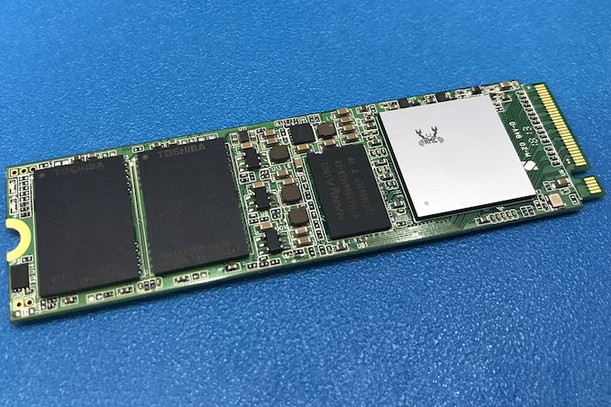
While Realtek is best known in the enthusiast space for for its peripheral controllers such as audio codecs and network controllers, the company also has a small-but-respectable SSD controller business that tends to fly under the radar due to its focus on entry-level and mainstream drives. But Realtek's stature in the SSD space is on the rise, as the company is not only planning new PCIe Gen5 SSD controllers, but also their first high-end, DRAM-equipped SSD controller.
For this year's Computex trade show, Realtek laid out a new SSD controller roadmap that calls for the company to release a trio of new SSD controllers over the next couple of years. First up is a new four-channel entry-level PCIe 4.0 controller, the RTS5776DL, which will be joined a bit later by a PCIe 5.0 variant, the RTS5781DL. But most interesting on Realtek's new roadmap is the final chip being planned: the eight-channel, DRAM-equipped RTS5782, which would be the company's first high-end SSD controller, capable of hitting sequential read rates as high as 14GB/second.
| Realtek NVMe SSD Controller Comparison | |||||||||
| RTS5782 | RTS5781DL | RTS5776DL | RTS5772DL | RTS5766DL | |||||
| Market Segment | High-End | Mainstream | Entry-Level | ||||||
| Error Correction | 4K LDPC | 2K LDPC | |||||||
| DRAM | DDR4, LPDDR4(X) | No | No | No | No | ||||
| Host Interface | PCIe 5.0 x4 | PCIe 5.0 x4 | PCIe 4.0 x4 | PCIe 4.0 x4 | PCIe 3.0 x4 | ||||
| NVMe Version | NVMe 2.0 | NVMe 2.0 | NVMe 2.0 | NVMe 1.4 | NVMe 1.4 | ||||
| NAND Channels, Interface Speed | 8 ch, 3600 MT/s |
4 ch, 3600 MT/s |
4 ch, 3600 MT/s |
8 ch, 1600 MT/s |
4 ch, 1200 MT/s |
||||
| Sequential Read | 14 GB/s | 10 GB/s | 7.4 GB/s | 6 GB/s | 3.2 GB/s | ||||
| Sequential Write | 12 GB/s | 10 GB/s | 7.4 GB/s | 6 GB/s | 2.2 GB/s | ||||
| 4KB Random Read IOPS | 2500k | 1400k | 1200k | - | - | ||||
| 4KB Random Write IOPS | 2500k | 1400k | 1200k | - | - | ||||
Diving a bit deeper into Realtek's roadmap, the RTS5776DL is traditional DRAM-less PCIe Gen4 x4 controller with four NAND chann... SSDs

Lorem Ipsum is simply dummy text of the printing and typesetting industry. Lorem Ipsum has been the industry's.
In addition to revealing its roadmap and plans concerning its current leading-edge process technologies, TSMC also shared progress of its N2 node as part of its Symposiums 2024. The company's first 2nm-class fabrication node, and predominantly featuring gate-all-around transistors, according to TSMC N2 has almost achieved its target performance and yield goals, which places it on track to enter high-volume manufacturing in the second half of 2025.
TSMC states that 'N2 development is well on track and N2P is next.' In particular, gate-all-around nanosheet devices currently achieve over 90% of their expected performance, whereas yields of 256 Mb SRAM (32 MB) devices already exceeds 80%, depending on the batch. All of this for a node that is over a year away from mass production.
Meanwhile, average yield of a 256 Mb SRAM was around 70% as of March, 2024, up from around 35% in April, 2023. Device performance has also been improving with higher frequencies being achieved while keeping power consumption in check.
Chip designer interest towards TSMC's first 2nm-class gate-all-around nanosheet transistor-based technology is significant, too. The number of new tape-outs (NTOs) in the first year of N2 is over two-times higher than it was for N5. Though with that said, given TSMC's close working relationship with a handful of high-volume vendors – most notably Appe – NTOs can be a very misleading figure since the first year of a new node at TSMC is capacity constrained, and consequently the bulk of that capacity goes to TSMC's priority partners.
Meanwhile, there were considerably more N5 tapeouts in its second year (some where N5P, of course) and N2 promises to have 2.6X more NTOs in its second year. So the node indeed looks quite promising. In fact, based on TSMC's slides (which we're unfortunately not able to republish), N2 is more popular than N3 in terms of NTOs both in the first and the second years of existence.
When it comes to the second year of N2, in the second half of 2026 TSMC plans to roll out its N2P technology, which promises additional performance and power benefits. N2P is expected to improve frequency by 15% - 20%, reduce power consumption by 30% - 40%, and increase chip density by over 1.15 times compared to N3E, significant benefits to move to all-new GAA nanosheet transistors.
Finally, for those companies that need the best in performance, power, and density, TSMC is poised to offer their A16 process in 2026. That node will also bring in backside power delivery, which will add costs, but is expected to greatly improve performance efficiency and scaling.
Semiconductors


 with 108 MB of SRAM to deliver 262 FP8 TFLOPS at 1 GHz at 160W thermal design power. A single-chip Wormhole n150 card carries 12 GB of GDDR6 memory featuring a 288 GB/s bandwidth.</p>
<p>Wormhole processors offer flexible scalability to meet the varying needs of workloads. In a standard workstation setup with four Wormhole n300 cards, the processors can merge to function as a single unit, appearing as a unified, extensive network of Tensix cores to the software. This configuration allows the accelerators to either work on the same workload, be divided among four developers or run up to eight distinct AI models simultaneously. A crucial feature of this scalability is that it operates natively without the need for virtualization. In data center environments, Wormhole processors will scale both inside one machine using PCIe or outside of a single machine using Ethernet. </p>
<p>From performance standpoint, Tenstorrent's single-chip Wormhole n150 card (72 Tensix cores at 1 GHz, 108 MB SRAM, 12 GB GDDR6 at 288 GB/s) is capable of 262 FP8 TFLOPS at 160W, whereas the dual-chip Wormhole n300 board (128 Tensix cores at 1 GHz, 192 MB SRAM, aggregated 24 GB GDDR6 at 576 GB/s) can offer up to 466 FP8 TFLOPS at 300W (according to <a href="https://www.tomshardware.com/pc-components/gpus/tenstorrents-risc-v-based-wormhole-ai-accelerators-are-available-for-pre-order-today-pre-built-workstations-start-at-dollar12000">Tom's Hardware</a>).</p>
<p style="text-align: center;"><a href="https://www.anandtech.com/show/21482/tenstorrent-launches-wormhole-ai-processors-466-fp8-tflops-at-300w"><img alt="" src="https://images.anandtech.com/doci/21482/tesntorrent-wormhole_575px.jpg" /></a></p>
<p>To put that 466 FP8 TFLOPS at 300W number into context, let's compare it to what AI market leader Nvidia has to offer at this thermal design power. Nvidia's A100 does not support FP8, but it does support INT8 and its peak performance is 624 TOPS (1,248 TOPS with sparsity). By contrast, Nvidia's H100 supports FP8 and its peak performance is massive 1,670 TFLOPS (3,341 TFLOPS with sparsity) at 300W, which is a big difference from Tenstorrent's Wormhole n300. </p>
<p>There is a big catch though. Tenstorrent's Wormhole n150 is offered for $999, whereas n300 is available for $1,399. By contrast, one Nvidia H100 card can retail for $30,000, depending on quantities. Of course, we do not know whether four or eight Wormhole processors can indeed deliver the performance of a single H300, though they will do so at 600W or 1200W TDP, respectively.</p>
<p>In addition to cards, Tenstorrent offers developers pre-built workstations with four n300 cards inside the less expensive Xeon-based TT-LoudBox with active cooling and a premium EPYC-powered TT-QuietBox with liquid cooling.</p>
<p>Sources: <a href="https://tenstorrent.com/vision/tenstorrent-launches-next-generation-wormhole-based-developer-kits-and-workstations">Tenstorrent</a>, <a href="https://www.tomshardware.com/pc-components/gpus/tenstorrents-risc-v-based-wormhole-ai-accelerators-are-available-for-pre-order-today-pre-built-workstations-start-at-dollar12000">Tom's Hardware</a></p>
</p> AI)
 with 108 MB of SRAM to deliver 262 FP8 TFLOPS at 1 GHz at 160W thermal design power. A single-chip Wormhole n150 card carries 12 GB of GDDR6 memory featuring a 288 GB/s bandwidth.</p>
<p>Wormhole processors offer flexible scalability to meet the varying needs of workloads. In a standard workstation setup with four Wormhole n300 cards, the processors can merge to function as a single unit, appearing as a unified, extensive network of Tensix cores to the software. This configuration allows the accelerators to either work on the same workload, be divided among four developers or run up to eight distinct AI models simultaneously. A crucial feature of this scalability is that it operates natively without the need for virtualization. In data center environments, Wormhole processors will scale both inside one machine using PCIe or outside of a single machine using Ethernet. </p>
<p>From performance standpoint, Tenstorrent's single-chip Wormhole n150 card (72 Tensix cores at 1 GHz, 108 MB SRAM, 12 GB GDDR6 at 288 GB/s) is capable of 262 FP8 TFLOPS at 160W, whereas the dual-chip Wormhole n300 board (128 Tensix cores at 1 GHz, 192 MB SRAM, aggregated 24 GB GDDR6 at 576 GB/s) can offer up to 466 FP8 TFLOPS at 300W (according to <a href="https://www.tomshardware.com/pc-components/gpus/tenstorrents-risc-v-based-wormhole-ai-accelerators-are-available-for-pre-order-today-pre-built-workstations-start-at-dollar12000">Tom's Hardware</a>).</p>
<p style="text-align: center;"><a href="https://www.anandtech.com/show/21482/tenstorrent-launches-wormhole-ai-processors-466-fp8-tflops-at-300w"><img alt="" src="https://images.anandtech.com/doci/21482/tesntorrent-wormhole_575px.jpg" /></a></p>
<p>To put that 466 FP8 TFLOPS at 300W number into context, let's compare it to what AI market leader Nvidia has to offer at this thermal design power. Nvidia's A100 does not support FP8, but it does support INT8 and its peak performance is 624 TOPS (1,248 TOPS with sparsity). By contrast, Nvidia's H100 supports FP8 and its peak performance is massive 1,670 TFLOPS (3,341 TFLOPS with sparsity) at 300W, which is a big difference from Tenstorrent's Wormhole n300. </p>
<p>There is a big catch though. Tenstorrent's Wormhole n150 is offered for $999, whereas n300 is available for $1,399. By contrast, one Nvidia H100 card can retail for $30,000, depending on quantities. Of course, we do not know whether four or eight Wormhole processors can indeed deliver the performance of a single H300, though they will do so at 600W or 1200W TDP, respectively.</p>
<p>In addition to cards, Tenstorrent offers developers pre-built workstations with four n300 cards inside the less expensive Xeon-based TT-LoudBox with active cooling and a premium EPYC-powered TT-QuietBox with liquid cooling.</p>
<p>Sources: <a href="https://tenstorrent.com/vision/tenstorrent-launches-next-generation-wormhole-based-developer-kits-and-workstations">Tenstorrent</a>, <a href="https://www.tomshardware.com/pc-components/gpus/tenstorrents-risc-v-based-wormhole-ai-accelerators-are-available-for-pre-order-today-pre-built-workstations-start-at-dollar12000">Tom's Hardware</a></p>
</p> AI)
 with 108 MB of SRAM to deliver 262 FP8 TFLOPS at 1 GHz at 160W thermal design power. A single-chip Wormhole n150 card carries 12 GB of GDDR6 memory featuring a 288 GB/s bandwidth.</p>
<p>Wormhole processors offer flexible scalability to meet the varying needs of workloads. In a standard workstation setup with four Wormhole n300 cards, the processors can merge to function as a single unit, appearing as a unified, extensive network of Tensix cores to the software. This configuration allows the accelerators to either work on the same workload, be divided among four developers or run up to eight distinct AI models simultaneously. A crucial feature of this scalability is that it operates natively without the need for virtualization. In data center environments, Wormhole processors will scale both inside one machine using PCIe or outside of a single machine using Ethernet. </p>
<p>From performance standpoint, Tenstorrent's single-chip Wormhole n150 card (72 Tensix cores at 1 GHz, 108 MB SRAM, 12 GB GDDR6 at 288 GB/s) is capable of 262 FP8 TFLOPS at 160W, whereas the dual-chip Wormhole n300 board (128 Tensix cores at 1 GHz, 192 MB SRAM, aggregated 24 GB GDDR6 at 576 GB/s) can offer up to 466 FP8 TFLOPS at 300W (according to <a href="https://www.tomshardware.com/pc-components/gpus/tenstorrents-risc-v-based-wormhole-ai-accelerators-are-available-for-pre-order-today-pre-built-workstations-start-at-dollar12000">Tom's Hardware</a>).</p>
<p style="text-align: center;"><a href="https://www.anandtech.com/show/21482/tenstorrent-launches-wormhole-ai-processors-466-fp8-tflops-at-300w"><img alt="" src="https://images.anandtech.com/doci/21482/tesntorrent-wormhole_575px.jpg" /></a></p>
<p>To put that 466 FP8 TFLOPS at 300W number into context, let's compare it to what AI market leader Nvidia has to offer at this thermal design power. Nvidia's A100 does not support FP8, but it does support INT8 and its peak performance is 624 TOPS (1,248 TOPS with sparsity). By contrast, Nvidia's H100 supports FP8 and its peak performance is massive 1,670 TFLOPS (3,341 TFLOPS with sparsity) at 300W, which is a big difference from Tenstorrent's Wormhole n300. </p>
<p>There is a big catch though. Tenstorrent's Wormhole n150 is offered for $999, whereas n300 is available for $1,399. By contrast, one Nvidia H100 card can retail for $30,000, depending on quantities. Of course, we do not know whether four or eight Wormhole processors can indeed deliver the performance of a single H300, though they will do so at 600W or 1200W TDP, respectively.</p>
<p>In addition to cards, Tenstorrent offers developers pre-built workstations with four n300 cards inside the less expensive Xeon-based TT-LoudBox with active cooling and a premium EPYC-powered TT-QuietBox with liquid cooling.</p>
<p>Sources: <a href="https://tenstorrent.com/vision/tenstorrent-launches-next-generation-wormhole-based-developer-kits-and-workstations">Tenstorrent</a>, <a href="https://www.tomshardware.com/pc-components/gpus/tenstorrents-risc-v-based-wormhole-ai-accelerators-are-available-for-pre-order-today-pre-built-workstations-start-at-dollar12000">Tom's Hardware</a></p>
</p> AI | https://compbuddey.blogspot.com/2024/08/tenstorrent-launches-wormhole-ai_4.html)
 with 108 MB of SRAM to deliver 262 FP8 TFLOPS at 1 GHz at 160W thermal design power. A single-chip Wormhole n150 card carries 12 GB of GDDR6 memory featuring a 288 GB/s bandwidth.</p>
<p>Wormhole processors offer flexible scalability to meet the varying needs of workloads. In a standard workstation setup with four Wormhole n300 cards, the processors can merge to function as a single unit, appearing as a unified, extensive network of Tensix cores to the software. This configuration allows the accelerators to either work on the same workload, be divided among four developers or run up to eight distinct AI models simultaneously. A crucial feature of this scalability is that it operates natively without the need for virtualization. In data center environments, Wormhole processors will scale both inside one machine using PCIe or outside of a single machine using Ethernet. </p>
<p>From performance standpoint, Tenstorrent's single-chip Wormhole n150 card (72 Tensix cores at 1 GHz, 108 MB SRAM, 12 GB GDDR6 at 288 GB/s) is capable of 262 FP8 TFLOPS at 160W, whereas the dual-chip Wormhole n300 board (128 Tensix cores at 1 GHz, 192 MB SRAM, aggregated 24 GB GDDR6 at 576 GB/s) can offer up to 466 FP8 TFLOPS at 300W (according to <a href="https://www.tomshardware.com/pc-components/gpus/tenstorrents-risc-v-based-wormhole-ai-accelerators-are-available-for-pre-order-today-pre-built-workstations-start-at-dollar12000">Tom's Hardware</a>).</p>
<p style="text-align: center;"><a href="https://www.anandtech.com/show/21482/tenstorrent-launches-wormhole-ai-processors-466-fp8-tflops-at-300w"><img alt="" src="https://images.anandtech.com/doci/21482/tesntorrent-wormhole_575px.jpg" /></a></p>
<p>To put that 466 FP8 TFLOPS at 300W number into context, let's compare it to what AI market leader Nvidia has to offer at this thermal design power. Nvidia's A100 does not support FP8, but it does support INT8 and its peak performance is 624 TOPS (1,248 TOPS with sparsity). By contrast, Nvidia's H100 supports FP8 and its peak performance is massive 1,670 TFLOPS (3,341 TFLOPS with sparsity) at 300W, which is a big difference from Tenstorrent's Wormhole n300. </p>
<p>There is a big catch though. Tenstorrent's Wormhole n150 is offered for $999, whereas n300 is available for $1,399. By contrast, one Nvidia H100 card can retail for $30,000, depending on quantities. Of course, we do not know whether four or eight Wormhole processors can indeed deliver the performance of a single H300, though they will do so at 600W or 1200W TDP, respectively.</p>
<p>In addition to cards, Tenstorrent offers developers pre-built workstations with four n300 cards inside the less expensive Xeon-based TT-LoudBox with active cooling and a premium EPYC-powered TT-QuietBox with liquid cooling.</p>
<p>Sources: <a href="https://tenstorrent.com/vision/tenstorrent-launches-next-generation-wormhole-based-developer-kits-and-workstations">Tenstorrent</a>, <a href="https://www.tomshardware.com/pc-components/gpus/tenstorrents-risc-v-based-wormhole-ai-accelerators-are-available-for-pre-order-today-pre-built-workstations-start-at-dollar12000">Tom's Hardware</a></p>
</p> AI&body=https://compbuddey.blogspot.com/2024/08/tenstorrent-launches-wormhole-ai_4.html)


0 Comments