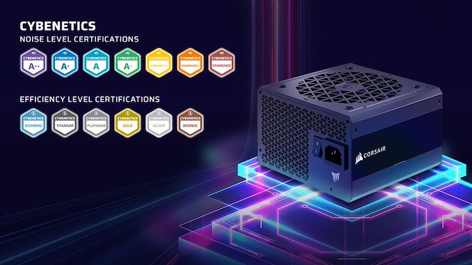

Corsair, a prominent figure in PC components, has announced a strategic shift in its approach to power supply unit (PSU) certifications. The company is dropping the widely recognized 80 PLUS certification in favor of the newer but more comprehensive Cybenetics certification.
According to the press release, the primary reason for Corsair’s move to Cybenetics certifications lies in the program's dual focus on both energy efficiency and noise levels. While the 80 PLUS certification has been a standard in the industry for decades, it exclusively measures energy conversion efficiency at four load levels (10%, 20%, 50%, 100%). Despite its long-standing presence, the 80 PLUS program has not seen significant updates in over 15 years, which limits its ability to provide a holistic view of PSU performance.
On the other hand, Cybenetics offers a more nuanced approach. It evaluates PSUs across multiple load levels and includes noise level assessments. This dual certification system rates efficiency on a familiar scale (Bronze to Titanium, plus a higher certification called Diamond) and noise levels from Standard (noisy) to A++ (virtually silent). By incorporating noise measurements, Cybenetics provides a more comprehensive overview of PSU performance, addressing an important aspect often overlooked by other certification programs. Cybenetics also enforces Power Factor, 5VSB efficiency, and Vampire Power thresholds, all important to the overall efficiency of a PSU.
Even though they're dropping 80 PLUS in favor of Cybernetics, Corsair is being highly diplomatic with their press release. They even suggest that the reader should not disregard either in favor of the other.
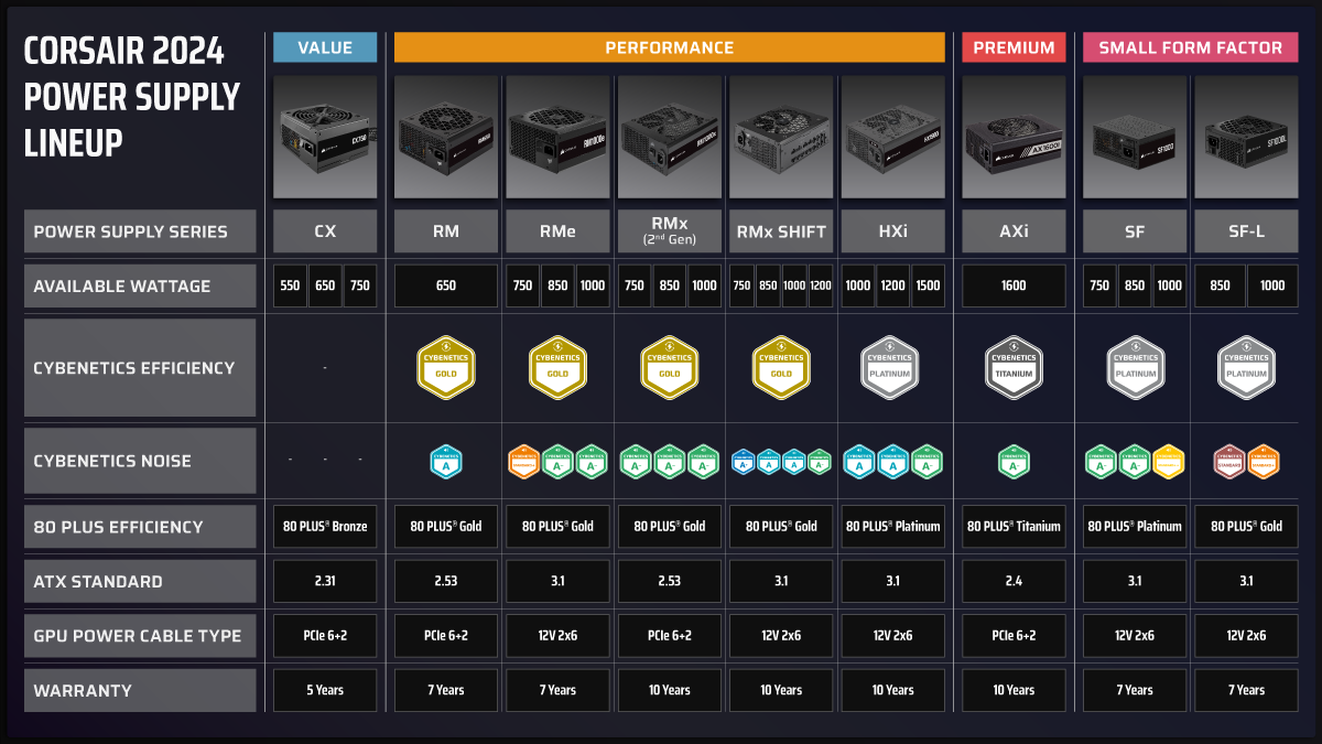
Our opinion is a bit harsher: the simplicity of the 80 PLUS certification program has led to two major flaws. First, manufacturers have primarily focused on maximizing efficiency at three specific load points, neglecting overall performance. Second, the majority of PSUs have clustered around the 80 PLUS Gold and Platinum certifications, with very few achieving the stringent Titanium level. This results in hundreds of PSUs with significantly different technical capabilities sharing the same certification badge, creating a misleading uniformity that fails to reflect true performance disparities.
Furthermore, almost every PSU platform that has been released over the past 15 years would achieve 80Plus Gold status or greater, with very few products falling down to the 80Plus Bronze certification and almost zero meeting the 80Plus White and 80Plus Silver requirements, making the three lowermost certifications practically defunct. Cybenetics dual certification certainly does not solve every issue and cannot fully assess everything there is to assess about a PSU, but it certainly makes much more information available to the user and allows users to at least factor in acoustics performance when purchasing a product.
The issue that seems to remain is that, due to the slackest requirements, manufacturers were almost always certifying their units with an input voltage of 115 VAC, resulting in myriads of units carrying a certification badge that would fail the same 80Plus certification requirements with an input voltage of 230 VAC. Unfortunately, this is also true for the Cybenetics standard, as the badges do not inform the user about the input voltage that the certification was attained with. However, as the Cybenetics standard revolves around average efficiency and not efficiency at specific load points, the majority of the PSUs should meet both efficiency thresholds and not the other way around.
Certification processes can be costly for manufacturers. By opting for the Cybenetics program, Corsair possibly aims to get the most value from its certification investments. Cybenetics offers more detailed and up-to-date testing methodologies, ensuring that the data provided is more reflective of real-world usage scenarios. In any case, Corsair’s shift to Cybenetics certification marks a significant development in the evaluation of PSUs and has the potential to create waves in the market.
Ultimately, this move has the potential disrupt the status quo. With Corsair's sheer size and influence in the larger power supply market, this could very well prompt other... Power Supply

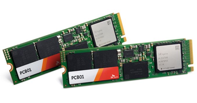
SK hynix early in Friday announced that the company has finished the development of it's PCB01 PCIe Gen5 SSD, the company's forthcoming high-end SSD for OEMs. Based on the company's new Alistar platform, the PCB01 is designed to deliver chart-topping performance for client machines. And, as a sign of the times, SK hynix is positioning the PCB01 for AI PCs, looking to synergize with the overall industry interest in anything and everything AI.
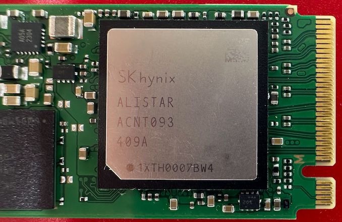
The bare, OEM-focused drives have previously been shown off by SK hynix, and make no attempt to hide what's under the hood. The PCB01 relies on SK hynix's Alistar controller, which features a PCIe Gen5 x4 host interface on the front end and eight NAND channels on the back end, placing it solidly in the realm of high-end SSDs. Paired with the Alistar controller is the company's latest 238-layer TLC NAND (H25T1TD48C & H25T2TD88C), which offers a maximum transfer speed of 2400 MT/second. Being that this is a high-end client SSD, there's also a DRAM chip on board, though the company isn't disclosing its capacity.
As with other high-end PCIe 5.0 client SSDs, SK hynix is planning on hitting peak read speeds of up to 14GB/second on the drive, while peak sequential write speeds should top 12GB/second (with pSLC caching, of course) – performance figures well within the realm of possibility for an 8 channel drive. As for random performance, at Computex the company was telling attendees that the drives should be able to sustain 4K random read and write rates of 2 million IOPS, which is very high as well. The SSDs are also said to consume up to 30% less power than 'predecessors,' according to SK hynix, though the company didn't elaborate on that figure. Typically in the storage industry, energy figures are based on iso-performance (rather than peak performance) – essentially measuring energy efficiency per bit rather than toal power consumption – and that is likely the case here as well.
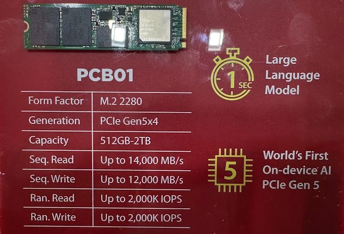
At least initially, SK Hynix plans to release its PCB01 in three capacities – 512 GB, 1 TB, and 2 TB. The company has previously disclosed that their 238L TLC NAND has a capacity of 512Gbit, so these are typical capacity figures for single-sided drives. And while the focus of the company's press release this week was on OEM drives, this is the same controller and NAND that is also going into the company's previously-teased retail Platinum P51 SSD, so this week's reveal offers a bit more detail into what to expect from that drive family as well.
Specs aside, Ahn Hyun, the Head of the N-S Committee at SK hynix, said that multiple global CPU providers for on-device AI PCs are seeking collaboration for the compatibility validation process, which is underway, so expect PCB01 drives inside PCs in this back-to-school and holiday seasons.
"We will work towards enhancing our leadership as the global top AI memory provider also in the NAND solution space by successfully completing the customer validation and mass production of PCB01, which will be in the limelight," Ahn Hyun said.
SSDs
Further to our last piece which we detailed Intel's issue to motherboard vendors to follow with stock power settings for Intel's 14th and 13th Gen Core series processors, Intel has now issued a follow-up statement to this. Over the last week or so, motherboard vendors quickly released firmware updates with a new profile called 'Intel Baseline', which motherboard vendors assumed would address the instability issues.
As it turns out, Intel doesn't seem to accept this as technically, these Intel Baseline profiles are not to be confused with Intel's default specifications. This means that Intel's Baseline profiles seemingly give the impression that they are operating at default settings, hence the terminology 'baseline' used, but this still opens motherboard vendors to use their interpretations of MCE or Multi-Core Enhancement.
To clarify things for consumers, Intel has sent us the following statement:
Several motherboard manufacturers have released BIOS profiles labeled ‘Intel Baseline Profile’. However, these BIOS profiles are not the same as the 'Intel Default Settings' recommendations that Intel has recently shared with its partners regarding the instability issues reported on 13th and 14th gen K SKU processors.
These ‘Intel Baseline Profile’ BIOS settings appear to be based on power delivery guidance previously provided by Intel to manufacturers describing the various power delivery options for 13th and 14th Generation K SKU processors based on motherboard capabilities.
Intel is not recommending motherboard manufacturers to use ‘baseline’ power delivery settings on boards capable of higher values.
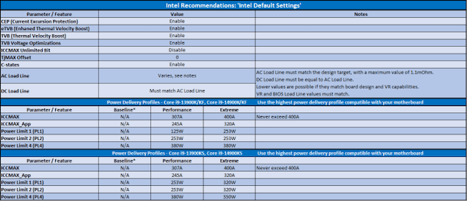
Intel’s recommended ‘Intel Default Settings’ are a combination of thermal and power delivery features along with a selection of possible power delivery profiles based on motherboard capabilities.
Intel recommends customers to implement the highest power delivery profile compatible with each individual motherboard design as noted in the table below:
Click to Enlarge Intel's Default Settings
What Intel's statement is effectively saying to consumers, is that users shouldn't be using the Baseline Power Delivery profiles which are offered by motherboard vendors through a plethora of firmware updates. Instead, Intel is recommending users opt for Intel Default Settings, which follows what the specific processor is rated for by Intel out of the box to achieve the clock speeds advertised, without users having to worry about firmware 'over' optimization which can cause instability as there have been many reports of happening.
Not only this, but the Intel Default settings offer a combination of thermal specifications and power capabilities, including voltage and frequency curve settings that apply to the capability of the motherboard used, and the power delivery equipped on the motherboard. At least for the most part, Intel is recommending users with 14th and 13th-Gen Core series K, KF, and KS SKUs that they do not recommend users opt in using the Baseline profiles offered by motherboard vendors.
Digesting the contrast between the two statements, the key differential is that Intel's priority is reducing the current going through the processor, which for both the 14th and 13th Gen Core series processors is a maximum of 400 A, even when using the Extreme profile. We know those motherboard vendors on their Z790 and Z690 motherboards opt for an unrestricted power profile, which is essentially 'unlimited' power and current to maximize performance at the cost of power consumption and heat, which does exacerbate problems and can lead to frequent bouts of instability, especially on high-intensity workloads.
Another variable Intel is recommending is that the AC Load Line must match the design target of the processor, with a maximum value of 1.1 mOhm, and that the DC Load Line must be ... CPUs


Kioxia's booth at FMS 2024 was a busy one with multiple technology demonstrations keeping visitors occupied. A walk-through of the BiCS 8 manufacturing process was the first to grab my attention. Kioxia and Western Digital announced the sampling of BiCS 8 in March 2023. We had touched briefly upon its CMOS Bonded Array (CBA) scheme in our coverage of Kioxial's 2Tb QLC NAND device and coverage of Western Digital's 128 TB QLC enterprise SSD proof-of-concept demonstration. At Kioxia's booth, we got more insights.

Traditionally, fabrication of flash chips involved placement of the associate logic circuitry (CMOS process) around the periphery of the flash array. The process then moved on to putting the CMOS under the cell array, but the wafer development process was serialized with the CMOS logic getting fabricated first followed by the cell array on top. However, this has some challenges because the cell array requires a high-temperature processing step to ensure higher reliability that can be detrimental to the health of the CMOS logic. Thanks to recent advancements in wafer bonding techniques, the new CBA process allows the CMOS wafer and cell array wafer to be processed independently in parallel and then pieced together, as shown in the models above.

The BiCS 8 3D NAND incorporates 218 layers, compared to 112 layers in BiCS 5 and 162 layers in BiCS 6. The company decided to skip over BiCS 7 (or, rather, it was probably a short-lived generation meant as an internal test vehicle). The generation retains the four-plane charge trap structure of BiCS 6. In its TLC avatar, it is available as a 1 Tbit device. The QLC version is available in two capacities - 1 Tbit and 2 Tbit.
Kioxia also noted that while the number of layers (218) doesn't compare favorably with the latest layer counts from the competition, its lateral scaling / cell shrinkage has enabled it to be competitive in terms of bit density as well as operating speeds (3200 MT/s). For reference, the latest shipping NAND from Micron - the G9 - has 276 layers with a bit density in TLC mode of 21 Gbit/mm2, and operates at up to 3600 MT/s. However, its 232L NAND operates only up to 2400 MT/s and has a bit density of 14.6 Gbit/mm2.
It must be noted that the CBA hybrid bonding process has advantages over the current processes used by other vendors - including Micron's CMOS under array (CuA) and SK hynix's 4D PUC (periphery-under-chip) developed in the late 2010s. It is expected that other NAND vendors will also move eventually to some variant of the hybrid bonding scheme used by Kioxia.
Storage
SK hynix early in Friday announced that the company has finished the development of it's PCB01 PCIe Gen5 SSD, the company's forthcoming high-end SSD for OEMs. Based on the company's new Alistar platform, the PCB01 is designed to deliver chart-topping performance for client machines. And, as a sign of the times, SK hynix is positioning the PCB01 for AI PCs, looking to synergize with the overall industry interest in anything and everything AI.
The bare, OEM-focused drives have previously been shown off by SK hynix, and make no attempt to hide what's under the hood. The PCB01 relies on SK hynix's Alistar controller, which features a PCIe Gen5 x4 host interface on the front end and eight NAND channels on the back end, placing it solidly in the realm of high-end SSDs. Paired with the Alistar controller is the company's latest 238-layer TLC NAND (H25T1TD48C & H25T2TD88C), which offers a maximum transfer speed of 2400 MT/second. Being that this is a high-end client SSD, there's also a DRAM chip on board, though the company isn't disclosing its capacity.
As with other high-end PCIe 5.0 client SSDs, SK hynix is planning on hitting peak read speeds of up to 14GB/second on the drive, while peak sequential write speeds should top 12GB/second (with pSLC caching, of course) – performance figures well within the realm of possibility for an 8 channel drive. As for random performance, at Computex the company was telling attendees that the drives should be able to sustain 4K random read and write rates of 2 million IOPS, which is very high as well. The SSDs are also said to consume up to 30% less power than 'predecessors,' according to SK hynix, though the company didn't elaborate on that figure. Typically in the storage industry, energy figures are based on iso-performance (rather than peak performance) – essentially measuring energy efficiency per bit rather than toal power consumption – and that is likely the case here as well.
At least initially, SK Hynix plans to release its PCB01 in three capacities – 512 GB, 1 TB, and 2 TB. The company has previously disclosed that their 238L TLC NAND has a capacity of 512Gbit, so these are typical capacity figures for single-sided drives. And while the focus of the company's press release this week was on OEM drives, this is the same controller and NAND that is also going into the company's previously-teased retail Platinum P51 SSD, so this week's reveal offers a bit more detail into what to expect from that drive family as well.
Specs aside, Ahn Hyun, the Head of the N-S Committee at SK hynix, said that multiple global CPU providers for on-device AI PCs are seeking collaboration for the compatibility validation process, which is underway, so expect PCB01 drives inside PCs in this back-to-school and holiday seasons.
"We will work towards enhancing our leadership as the global top AI memory provider also in the NAND solution space by successfully completing the customer validation and mass production of PCB01, which will be in the limelight," Ahn Hyun said.
SSDs
Further to our last piece which we detailed Intel's issue to motherboard vendors to follow with stock power settings for Intel's 14th and 13th Gen Core series processors, Intel has now issued a follow-up statement to this. Over the last week or so, motherboard vendors quickly released firmware updates with a new profile called 'Intel Baseline', which motherboard vendors assumed would address the instability issues.
As it turns out, Intel doesn't seem to accept this as technically, these Intel Baseline profiles are not to be confused with Intel's default specifications. This means that Intel's Baseline profiles seemingly give the impression that they are operating at default settings, hence the terminology 'baseline' used, but this still opens motherboard vendors to use their interpretations of MCE or Multi-Core Enhancement.
To clarify things for consumers, Intel has sent us the following statement:
Several motherboard manufacturers have released BIOS profiles labeled ‘Intel Baseline Profile’. However, these BIOS profiles are not the same as the 'Intel Default Settings' recommendations that Intel has recently shared with its partners regarding the instability issues reported on 13th and 14th gen K SKU processors.
These ‘Intel Baseline Profile’ BIOS settings appear to be based on power delivery guidance previously provided by Intel to manufacturers describing the various power delivery options for 13th and 14th Generation K SKU processors based on motherboard capabilities.
Intel is not recommending motherboard manufacturers to use ‘baseline’ power delivery settings on boards capable of higher values.
Intel’s recommended ‘Intel Default Settings’ are a combination of thermal and power delivery features along with a selection of possible power delivery profiles based on motherboard capabilities.
Intel recommends customers to implement the highest power delivery profile compatible with each individual motherboard design as noted in the table below:
Click to Enlarge Intel's Default Settings
What Intel's statement is effectively saying to consumers, is that users shouldn't be using the Baseline Power Delivery profiles which are offered by motherboard vendors through a plethora of firmware updates. Instead, Intel is recommending users opt for Intel Default Settings, which follows what the specific processor is rated for by Intel out of the box to achieve the clock speeds advertised, without users having to worry about firmware 'over' optimization which can cause instability as there have been many reports of happening.
Not only this, but the Intel Default settings offer a combination of thermal specifications and power capabilities, including voltage and frequency curve settings that apply to the capability of the motherboard used, and the power delivery equipped on the motherboard. At least for the most part, Intel is recommending users with 14th and 13th-Gen Core series K, KF, and KS SKUs that they do not recommend users opt in using the Baseline profiles offered by motherboard vendors.
Digesting the contrast between the two statements, the key differential is that Intel's priority is reducing the current going through the processor, which for both the 14th and 13th Gen Core series processors is a maximum of 400 A, even when using the Extreme profile. We know those motherboard vendors on their Z790 and Z690 motherboards opt for an unrestricted power profile, which is essentially 'unlimited' power and current to maximize performance at the cost of power consumption and heat, which does exacerbate problems and can lead to frequent bouts of instability, especially on high-intensity workloads.
Another variable Intel is recommending is that the AC Load Line must match the design target of the processor, with a maximum value of 1.1 mOhm, and that the DC Load Line must be ... CPUs
Kioxia's booth at FMS 2024 was a busy one with multiple technology demonstrations keeping visitors occupied. A walk-through of the BiCS 8 manufacturing process was the first to grab my attention. Kioxia and Western Digital announced the sampling of BiCS 8 in March 2023. We had touched briefly upon its CMOS Bonded Array (CBA) scheme in our coverage of Kioxial's 2Tb QLC NAND device and coverage of Western Digital's 128 TB QLC enterprise SSD proof-of-concept demonstration. At Kioxia's booth, we got more insights.
Traditionally, fabrication of flash chips involved placement of the associate logic circuitry (CMOS process) around the periphery of the flash array. The process then moved on to putting the CMOS under the cell array, but the wafer development process was serialized with the CMOS logic getting fabricated first followed by the cell array on top. However, this has some challenges because the cell array requires a high-temperature processing step to ensure higher reliability that can be detrimental to the health of the CMOS logic. Thanks to recent advancements in wafer bonding techniques, the new CBA process allows the CMOS wafer and cell array wafer to be processed independently in parallel and then pieced together, as shown in the models above.
The BiCS 8 3D NAND incorporates 218 layers, compared to 112 layers in BiCS 5 and 162 layers in BiCS 6. The company decided to skip over BiCS 7 (or, rather, it was probably a short-lived generation meant as an internal test vehicle). The generation retains the four-plane charge trap structure of BiCS 6. In its TLC avatar, it is available as a 1 Tbit device. The QLC version is available in two capacities - 1 Tbit and 2 Tbit.
Kioxia also noted that while the number of layers (218) doesn't compare favorably with the latest layer counts from the competition, its lateral scaling / cell shrinkage has enabled it to be competitive in terms of bit density as well as operating speeds (3200 MT/s). For reference, the latest shipping NAND from Micron - the G9 - has 276 layers with a bit density in TLC mode of 21 Gbit/mm2, and operates at up to 3600 MT/s. However, its 232L NAND operates only up to 2400 MT/s and has a bit density of 14.6 Gbit/mm2.
It must be noted that the CBA hybrid bonding process has advantages over the current processes used by other vendors - including Micron's CMOS under array (CuA) and SK hynix's 4D PUC (periphery-under-chip) developed in the late 2010s. It is expected that other NAND vendors will also move eventually to some variant of the hybrid bonding scheme used by Kioxia.
Storage
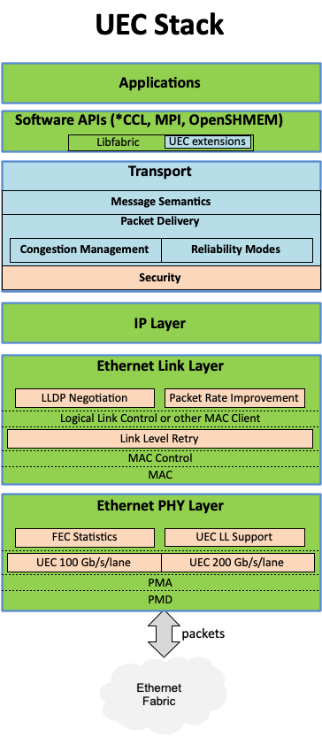
The Ultra Ethernet Consortium (UEC) has announced this week that the next-generation interconnection consortium has grown to 55 members. And as the group works towards developing the initial version of their ultra-fast Ethernet standard, they have released some of the first technical details on the upcoming standard.
Formed in the summer of 2023, the UEC aims to develop a new standard for interconnection for AI and HPC datacenter needs, serving as a de-facto (if not de-jure) alternative to InfiniBand, which is largely under the control of NVIDIA these days. The UEC began to accept new members back in November, and just in five months' time it gained 45 new members, which highlights massive interest for the new technology. The consortium now boasts 55 members and 715 industry experts, who are working across eight technical groups.
There is a lot of work at hand for the UEC, as the group has laid out in their latest development blog post, as the consortium works to to build a unified Ethernet-based communication stack for high-performance networking supporting artificial intelligence and high-performance computing clusters. The consortium's technical objectives include developing specifications, APIs, and source code for Ultra Ethernet communications, updating existing protocols, and introducing new mechanisms for telemetry, signaling, security, and congestion management. In particular, Ultra Ethernet introduces the UEC Transport (UET) for higher network utilization and lower tail latency to speed up RDMA (Remote Direct Memory Access) operation over Ethernet. Key features include multi-path packet spraying, flexible ordering, and advanced congestion control, ensuring efficient and reliable data transfer.
These enhancements are designed to address the needs of large AI and HPC clusters — with separate profiles for each type of deployment — though everything is done in a surgical manner to enhance the technology, but reuse as much of the existing Ethernet as possible to maintain cost efficiency and interoperability.
The consortium's founding members include AMD, Arista, Broadcom, Cisco, Eviden (an Atos Business), HPE, Intel, Meta, and Microsoft. After the Ultra Ethernet Consortium (UEC) began to accept new members in October, 2023, numerous industry heavyweights have joined the group, including Baidu, Dell, Huawei, IBM, Nokia, Lenovo, Supermicro, and Tencent.
The consortium currently plans to release the initial 1.0 version of the UEC specification publicly sometime in the third quarter of 2024.
"There was always a recognition that UEC was meeting a need in the industry," said J Metz, Chair of the UEC Steering Committee. "There is a strong desire to have an open, accessible, Ethernet-based network specifically designed to accommodate AI and HPC workload requirements. This level of involvement is encouraging; it helps us achieve the goal of broad interoperability and stability."
While it is evident that then Ultra Ethernet Consortium is gaining support across the industry, it is still unclear where other industry behemoths like AWS and Google stand. While the hardware companies involved can design Ultra Ethernet support into their hardware and systems, the technology ultimately exists to serve large datacenter and HPC system operators. So it will be interesting to see what interest they take in (and how quickly they adopt) the nascent Ethernet backbone technology once hardware incorporating it is ready.
Networking
![]()
In addition to revealing its roadmap and plans concerning its current leading-edge process technologies, TSMC also shared progress of its N2 node as part of its Symposiums 2024. The company's first 2nm-class fabrication node, and predominantly featuring gate-all-around transistors, according to TSMC N2 has almost achieved its target performance and yield goals, which places it on track to enter high-volume manufacturing in the second half of 2025.
TSMC states that 'N2 development is well on track and N2P is next.' In particular, gate-all-around nanosheet devices currently achieve over 90% of their expected performance, whereas yields of 256 Mb SRAM (32 MB) devices already exceeds 80%, depending on the batch. All of this for a node that is over a year away from mass production.
Meanwhile, average yield of a 256 Mb SRAM was around 70% as of March, 2024, up from around 35% in April, 2023. Device performance has also been improving with higher frequencies being achieved while keeping power consumption in check.
Chip designer interest towards TSMC's first 2nm-class gate-all-around nanosheet transistor-based technology is significant, too. The number of new tape-outs (NTOs) in the first year of N2 is over two-times higher than it was for N5. Though with that said, given TSMC's close working relationship with a handful of high-volume vendors – most notably Appe – NTOs can be a very misleading figure since the first year of a new node at TSMC is capacity constrained, and consequently the bulk of that capacity goes to TSMC's priority partners.
Meanwhile, there were considerably more N5 tapeouts in its second year (some where N5P, of course) and N2 promises to have 2.6X more NTOs in its second year. So the node indeed looks quite promising. In fact, based on TSMC's slides (which we're unfortunately not able to republish), N2 is more popular than N3 in terms of NTOs both in the first and the second years of existence.
When it comes to the second year of N2, in the second half of 2026 TSMC plans to roll out its N2P technology, which promises additional performance and power benefits. N2P is expected to improve frequency by 15% - 20%, reduce power consumption by 30% - 40%, and increase chip density by over 1.15 times compared to N3E, significant benefits to move to all-new GAA nanosheet transistors.
Finally, for those companies that need the best in performance, power, and density, TSMC is poised to offer their A16 process in 2026. That node will also bring in backside power delivery, which will add costs, but is expected to greatly improve performance efficiency and scaling.
Semiconductors![Rapidus Wants to Offer Fully Automated Packaging for 2nm Fab to Cut Chip Lead Times <p align="center"><a href="https://www.anandtech.com/show/21525/rapidus-2nm-fully-automated-chip-packaging-to-cut-lead-times"><img src="https://images.anandtech.com/doci/21525/intel-foundry-wafer-semiconductor-fab-ifs-678_575px.jpg" alt="" /></a></p><p><p>One of the core challenges that Rapidus will face when it kicks off volume production of chips on its 2nm-class process technology in 2027 is lining up customers. With Intel, Samsung, and TSMC all slated to offer their own 2nm-class nodes by that time, Rapidus will need some kind of advantage to attract customers away from its more established rivals. To that end, the company thinks they've found their edge: fully automated packaging that will allow for shorter chip lead times than manned packaging operations.</p>
<p>In an interview with <a href="https://asia.nikkei.com/Editor-s-Picks/Interview/Japan-s-Rapidus-to-fully-automate-2-nm-chip-fab-president-says">Nikkei</a>, Rapidus' president, Atsuyoshi Koike, outlined the company's vision to use advanced packaging as a competitive edge for the new fab. <a href="https://www.anandtech.com/show/21411/rapidus-adds-chip-packaging-services-to-plans-for-32b-2nm-fab">The Hokkaido facility</a>, which is currently under construction and is expecting to begin equipment installation this December, is already slated to both produce chips and offer advanced packaging services within the same facility, an industry first. But ultimately, Rapidus biggest plan to differentiate itself is by automating the back-end fab processes (chip packaging) to provide significantly faster turnaround times.</p>
<p>Rapidus is targetting back-end production in particular as, compared to front-end (lithography) production, back-end production still heavily relies on human labor. No other advanced packaging fab has fully automated the process thus far, which provides for a degree of flexibility, but slows throughput. But with automation in place to handle this aspect of chip production, Rapidus would be able to increase chip packaging efficiency and speed, which is crucial as chip assembly tasks become more complex. Rapidus is also collaborating with multiple Japanese suppliers to source materials for back-end production. </p>
<p>"In the past, Japanese chipmakers tried to keep their technology development exclusively in-house, which pushed up development costs and made them less competitive," Koike told Nikkei. "[Rapidus plans to] open up technology that should be standardized, bringing down costs, while handling important technology in-house." </p>
<p>Financially, Rapidus faces a significant challenge, needing a total of ¥5 trillion ($35 billion) by the time mass production starts in 2027. The company estimates that ¥2 trillion will be required by 2025 for prototype production. While the Japanese government has provided ¥920 billion in aid, Rapidus still needs to secure substantial funding from private investors.</p>
<p>Due to its lack of track record and experience of chip production as. well as limited visibility for success, Rapidus is finding it difficult to attract private financing. The company is in discussions with the government to make it easier to raise capital, including potential loan guarantees, and is hopeful that new legislation will assist in this effort.</p>
</p> Semiconductors](https://lh3.googleusercontent.com/blogger_img_proxy/AEn0k_t637H2758y5zuWd0dX4Cqax8XFfcVqqRRx5O1omX3BaSQp-SMB4tJcHQTLcf5-vGQs4ZwGzLmqbkuxZZQLl3cA1fUKBv39MgFOy4D2cnrT5x6XkdnIkoJ57TW89ksmgXEqmN6KVqfU1lRUwO4fVsPcX-xdy-8dmmBaG0m7WJ30UBJA=w72-h72-p-k-no-nu)
One of the core challenges that Rapidus will face when it kicks off volume production of chips on its 2nm-class process technology in 2027 is lining up customers. With Intel, Samsung, and TSMC all slated to offer their own 2nm-class nodes by that time, Rapidus will need some kind of advantage to attract customers away from its more established rivals. To that end, the company thinks they've found their edge: fully automated packaging that will allow for shorter chip lead times than manned packaging operations.
In an interview with Nikkei, Rapidus' president, Atsuyoshi Koike, outlined the company's vision to use advanced packaging as a competitive edge for the new fab. The Hokkaido facility, which is currently under construction and is expecting to begin equipment installation this December, is already slated to both produce chips and offer advanced packaging services within the same facility, an industry first. But ultimately, Rapidus biggest plan to differentiate itself is by automating the back-end fab processes (chip packaging) to provide significantly faster turnaround times.
Rapidus is targetting back-end production in particular as, compared to front-end (lithography) production, back-end production still heavily relies on human labor. No other advanced packaging fab has fully automated the process thus far, which provides for a degree of flexibility, but slows throughput. But with automation in place to handle this aspect of chip production, Rapidus would be able to increase chip packaging efficiency and speed, which is crucial as chip assembly tasks become more complex. Rapidus is also collaborating with multiple Japanese suppliers to source materials for back-end production.
"In the past, Japanese chipmakers tried to keep their technology development exclusively in-house, which pushed up development costs and made them less competitive," Koike told Nikkei. "[Rapidus plans to] open up technology that should be standardized, bringing down costs, while handling important technology in-house."
Financially, Rapidus faces a significant challenge, needing a total of ¥5 trillion ($35 billion) by the time mass production starts in 2027. The company estimates that ¥2 trillion will be required by 2025 for prototype production. While the Japanese government has provided ¥920 billion in aid, Rapidus still needs to secure substantial funding from private investors.
Due to its lack of track record and experience of chip production as. well as limited visibility for success, Rapidus is finding it difficult to attract private financing. The company is in discussions with the government to make it easier to raise capital, including potential loan guarantees, and is hopeful that new legislation will assist in this effort.
Semiconductors
Enermax, established in 1990, is a renowned Taiwanese company in the PC hardware industry, particularly recognized for its innovative power supply units (PSUs), cooling solutions, and PC cases. Over the years, Enermax has built a reputation for engineering reliable, high-performance PSUs that primarily target enthusiasts and professional users. Their commitment to quality and technological advancement has kept them at the forefront of the industry, constantly evolving to meet the demands of the ever-changing tech landscape.
In this review, we are looking at the latest addition to Enermax's impressive PSU lineup: the Revolution D.F. 12 750W PSU. This is the second ATX 3.1-compliant power supply to arrive in our labs, and, broadly speaking, illustrates how we're approaching the inflection point for PSU vendors to update their designs for Intel's revised PSU standard.
As for the Revolution D.F. 12 itself, Enermax's new PSU pursues a balanced design, meeting modern gaming PCs mid-way with good conversion efficiency and an overall robust power delivery system. With features like fully modular cables with per-wire sleeving, a dynamic hybrid fan control for optimal cooling, and advanced topologies, the Revolution D.F. 12 750W is primed to deliver on both reliability and performance. We will delve into its specifications, build quality, and performance metrics to see if the new unit lives up to Enermax's esteemed legacy.
Cases/Cooling/PSUs

When Western Digital introduced its Ultrastar DC SN861 SSDs earlier this year, the company did not disclose which controller it used for these drives, which made many observers presume that WD was using an in-house controller. But a recent teardown of the drive shows that is not the case; instead, the company is using a controller from Fadu, a South Korean company founded in 2015 that specializes on enterprise-grade turnkey SSD solutions.
The Western Digital Ultrastar DC SN861 SSD is aimed at performance-hungry hyperscale datacenters and enterprise customers which are adopting PCIe Gen5 storage devices these days. And, as uncovered in photos from a recent Storage Review article, the drive is based on Fadu's FC5161 NVMe 2.0-compliant controller. The FC5161 utilizes 16 NAND channels supporting an ONFi 5.0 2400 MT/s interface, and features a combination of enterprise-grade capabilities (OCP Cloud Spec 2.0, SR-IOV, up to 512 name spaces for ZNS support, flexible data placement, NVMe-MI 1.2, advanced security, telemetry, power loss protection) not available on other off-the-shelf controllers – or on any previous Western Digital controllers.
The Ultrastar DC SN861 SSD offers sequential read speeds up to 13.7 GB/s as well as sequential write speeds up to 7.5 GB/s. As for random performance, it boasts with an up to 3.3 million random 4K read IOPS and up to 0.8 million random 4K write IOPS. The drives are available in capacities between 1.6 TB and 7.68 TB with one or three drive writes per day (DWPD) over five years rating as well as in U.2 and E1.S form-factors.
While the two form factors of the SN861 share a similar technical design, Western Digital has tailored each version for distinct workloads: the E1.S supports FDP and performance enhancements specifically for cloud environments. By contrast, the U.2 model is geared towards high-performance enterprise tasks and emerging applications like AI.
Without any doubts, Western Digital's Ultrastar DC SN861 is a feature-rich high-performance enterprise-grade SSD. It has another distinctive feature: a 5W idle power consumption, which is rather low by the standards of enterprise-grade drives (e.g., it is 1W lower compared to the SN840). While the difference with predecessors may be just 1W, hyperscalers deploy thousands of drives and for their TCO every watt counts.
Western Digital's Ultrastar DC SN861 SSDs are now available for purchase to select customers (such as Meta) and to interested parties. Prices are unknown, but they will depend on such factors as volumes.
Sources: Fadu, Storage Review
Storage
Lorem Ipsum is simply dummy text of the printing and typesetting industry. Lorem Ipsum has been the industry's.
SK hynix early in Friday announced that the company has finished the development of it's PCB01 PCIe Gen5 SSD, the company's forthcoming high-end SSD for OEMs. Based on the company's new Alistar platform, the PCB01 is designed to deliver chart-topping performance for client machines. And, as a sign of the times, SK hynix is positioning the PCB01 for AI PCs, looking to synergize with the overall industry interest in anything and everything AI.
The bare, OEM-focused drives have previously been shown off by SK hynix, and make no attempt to hide what's under the hood. The PCB01 relies on SK hynix's Alistar controller, which features a PCIe Gen5 x4 host interface on the front end and eight NAND channels on the back end, placing it solidly in the realm of high-end SSDs. Paired with the Alistar controller is the company's latest 238-layer TLC NAND (H25T1TD48C & H25T2TD88C), which offers a maximum transfer speed of 2400 MT/second. Being that this is a high-end client SSD, there's also a DRAM chip on board, though the company isn't disclosing its capacity.
As with other high-end PCIe 5.0 client SSDs, SK hynix is planning on hitting peak read speeds of up to 14GB/second on the drive, while peak sequential write speeds should top 12GB/second (with pSLC caching, of course) – performance figures well within the realm of possibility for an 8 channel drive. As for random performance, at Computex the company was telling attendees that the drives should be able to sustain 4K random read and write rates of 2 million IOPS, which is very high as well. The SSDs are also said to consume up to 30% less power than 'predecessors,' according to SK hynix, though the company didn't elaborate on that figure. Typically in the storage industry, energy figures are based on iso-performance (rather than peak performance) – essentially measuring energy efficiency per bit rather than toal power consumption – and that is likely the case here as well.
At least initially, SK Hynix plans to release its PCB01 in three capacities – 512 GB, 1 TB, and 2 TB. The company has previously disclosed that their 238L TLC NAND has a capacity of 512Gbit, so these are typical capacity figures for single-sided drives. And while the focus of the company's press release this week was on OEM drives, this is the same controller and NAND that is also going into the company's previously-teased retail Platinum P51 SSD, so this week's reveal offers a bit more detail into what to expect from that drive family as well.
Specs aside, Ahn Hyun, the Head of the N-S Committee at SK hynix, said that multiple global CPU providers for on-device AI PCs are seeking collaboration for the compatibility validation process, which is underway, so expect PCB01 drives inside PCs in this back-to-school and holiday seasons.
"We will work towards enhancing our leadership as the global top AI memory provider also in the NAND solution space by successfully completing the customer validation and mass production of PCB01, which will be in the limelight," Ahn Hyun said.
SSDs
Further to our last piece which we detailed Intel's issue to motherboard vendors to follow with stock power settings for Intel's 14th and 13th Gen Core series processors, Intel has now issued a follow-up statement to this. Over the last week or so, motherboard vendors quickly released firmware updates with a new profile called 'Intel Baseline', which motherboard vendors assumed would address the instability issues.
As it turns out, Intel doesn't seem to accept this as technically, these Intel Baseline profiles are not to be confused with Intel's default specifications. This means that Intel's Baseline profiles seemingly give the impression that they are operating at default settings, hence the terminology 'baseline' used, but this still opens motherboard vendors to use their interpretations of MCE or Multi-Core Enhancement.
To clarify things for consumers, Intel has sent us the following statement:
Several motherboard manufacturers have released BIOS profiles labeled ‘Intel Baseline Profile’. However, these BIOS profiles are not the same as the 'Intel Default Settings' recommendations that Intel has recently shared with its partners regarding the instability issues reported on 13th and 14th gen K SKU processors.
These ‘Intel Baseline Profile’ BIOS settings appear to be based on power delivery guidance previously provided by Intel to manufacturers describing the various power delivery options for 13th and 14th Generation K SKU processors based on motherboard capabilities.
Intel is not recommending motherboard manufacturers to use ‘baseline’ power delivery settings on boards capable of higher values.
Intel’s recommended ‘Intel Default Settings’ are a combination of thermal and power delivery features along with a selection of possible power delivery profiles based on motherboard capabilities.
Intel recommends customers to implement the highest power delivery profile compatible with each individual motherboard design as noted in the table below:
Click to Enlarge Intel's Default Settings
What Intel's statement is effectively saying to consumers, is that users shouldn't be using the Baseline Power Delivery profiles which are offered by motherboard vendors through a plethora of firmware updates. Instead, Intel is recommending users opt for Intel Default Settings, which follows what the specific processor is rated for by Intel out of the box to achieve the clock speeds advertised, without users having to worry about firmware 'over' optimization which can cause instability as there have been many reports of happening.
Not only this, but the Intel Default settings offer a combination of thermal specifications and power capabilities, including voltage and frequency curve settings that apply to the capability of the motherboard used, and the power delivery equipped on the motherboard. At least for the most part, Intel is recommending users with 14th and 13th-Gen Core series K, KF, and KS SKUs that they do not recommend users opt in using the Baseline profiles offered by motherboard vendors.
Digesting the contrast between the two statements, the key differential is that Intel's priority is reducing the current going through the processor, which for both the 14th and 13th Gen Core series processors is a maximum of 400 A, even when using the Extreme profile. We know those motherboard vendors on their Z790 and Z690 motherboards opt for an unrestricted power profile, which is essentially 'unlimited' power and current to maximize performance at the cost of power consumption and heat, which does exacerbate problems and can lead to frequent bouts of instability, especially on high-intensity workloads.
Another variable Intel is recommending is that the AC Load Line must match the design target of the processor, with a maximum value of 1.1 mOhm, and that the DC Load Line must be ... CPUs

 certifications. The company is dropping the widely recognized 80 PLUS certification in favor of the newer but more comprehensive Cybenetics certification.</p>
<p>According to the <a href="https://www.corsair.com/newsroom/press-release/corsair-transitions-to-more-comprehensive-psu-certifications-from-cybenetics">press release</a>, the primary reason for Corsair’s move to Cybenetics certifications lies in the program's dual focus on both energy efficiency and noise levels. While the 80 PLUS certification has been a standard in the industry for decades, it exclusively measures energy conversion efficiency at four load levels (10%, 20%, 50%, 100%). Despite its long-standing presence, the 80 PLUS program has not seen significant updates in over 15 years, which limits its ability to provide a holistic view of PSU performance.</p>
<p>On the other hand, Cybenetics offers a more nuanced approach. It evaluates PSUs across multiple load levels and includes noise level assessments. This dual certification system rates efficiency on a familiar scale (Bronze to Titanium, plus a higher certification called Diamond) and noise levels from Standard (noisy) to A++ (virtually silent). By incorporating noise measurements, Cybenetics provides a more comprehensive overview of PSU performance, addressing an important aspect often overlooked by other certification programs. Cybenetics also enforces Power Factor, 5VSB efficiency, and Vampire Power thresholds, all important to the overall efficiency of a PSU.</p>
<p>Even though they're dropping 80 PLUS in favor of Cybernetics, Corsair is being highly diplomatic with their press release. They even suggest that the reader should not disregard either in favor of the other.</p>
<p align="center"><a href="https://www.anandtech.com/show/21511/corsair-transitions-to-cybenetics-certification-for-power-supplies"><img alt="" src="https://images.anandtech.com/doci/21511/Image_2024_PSU_Chart_PR.png" style="width: 100%;" /></a></p>
<p>Our opinion is a bit harsher: the simplicity of the 80 PLUS certification program has led to two major flaws. First, manufacturers have primarily focused on maximizing efficiency at three specific load points, neglecting overall performance. Second, the majority of PSUs have clustered around the 80 PLUS Gold and Platinum certifications, with very few achieving the stringent Titanium level. This results in hundreds of PSUs with significantly different technical capabilities sharing the same certification badge, creating a misleading uniformity that fails to reflect true performance disparities.</p>
<p>Furthermore, almost every PSU platform that has been released over the past 15 years would achieve 80Plus Gold status or greater, with very few products falling down to the 80Plus Bronze certification and almost zero meeting the 80Plus White and 80Plus Silver requirements, making the three lowermost certifications practically defunct. Cybenetics dual certification certainly does not solve every issue and cannot fully assess everything there is to assess about a PSU, but it certainly makes much more information available to the user and allows users to at least factor in acoustics performance when purchasing a product.</p>
<p>The issue that seems to remain is that, due to the slackest requirements, manufacturers were almost always certifying their units with an input voltage of 115 VAC, resulting in myriads of units carrying a certification badge that would fail the same 80Plus certification requirements with an input voltage of 230 VAC. Unfortunately, this is also true for the Cybenetics standard, as the badges do not inform the user about the input voltage that the certification was attained with. However, as the Cybenetics standard revolves around average efficiency and not efficiency at specific load points, the majority of the PSUs should meet both efficiency thresholds and not the other way around.</p>
<p>Certification processes can be costly for manufacturers. By opting for the Cybenetics program, Corsair possibly aims to get the most value from its certification investments. Cybenetics offers more detailed and up-to-date testing methodologies, ensuring that the data provided is more reflective of real-world usage scenarios. In any case, Corsair’s shift to Cybenetics certification marks a significant development in the evaluation of PSUs and has the potential to create waves in the market.</p>
<p>Ultimately, this move has the potential disrupt the status quo. With Corsair's sheer size and influence in the larger power supply market, this could very well prompt other... Power Supply)
 certifications. The company is dropping the widely recognized 80 PLUS certification in favor of the newer but more comprehensive Cybenetics certification.</p>
<p>According to the <a href="https://www.corsair.com/newsroom/press-release/corsair-transitions-to-more-comprehensive-psu-certifications-from-cybenetics">press release</a>, the primary reason for Corsair’s move to Cybenetics certifications lies in the program's dual focus on both energy efficiency and noise levels. While the 80 PLUS certification has been a standard in the industry for decades, it exclusively measures energy conversion efficiency at four load levels (10%, 20%, 50%, 100%). Despite its long-standing presence, the 80 PLUS program has not seen significant updates in over 15 years, which limits its ability to provide a holistic view of PSU performance.</p>
<p>On the other hand, Cybenetics offers a more nuanced approach. It evaluates PSUs across multiple load levels and includes noise level assessments. This dual certification system rates efficiency on a familiar scale (Bronze to Titanium, plus a higher certification called Diamond) and noise levels from Standard (noisy) to A++ (virtually silent). By incorporating noise measurements, Cybenetics provides a more comprehensive overview of PSU performance, addressing an important aspect often overlooked by other certification programs. Cybenetics also enforces Power Factor, 5VSB efficiency, and Vampire Power thresholds, all important to the overall efficiency of a PSU.</p>
<p>Even though they're dropping 80 PLUS in favor of Cybernetics, Corsair is being highly diplomatic with their press release. They even suggest that the reader should not disregard either in favor of the other.</p>
<p align="center"><a href="https://www.anandtech.com/show/21511/corsair-transitions-to-cybenetics-certification-for-power-supplies"><img alt="" src="https://images.anandtech.com/doci/21511/Image_2024_PSU_Chart_PR.png" style="width: 100%;" /></a></p>
<p>Our opinion is a bit harsher: the simplicity of the 80 PLUS certification program has led to two major flaws. First, manufacturers have primarily focused on maximizing efficiency at three specific load points, neglecting overall performance. Second, the majority of PSUs have clustered around the 80 PLUS Gold and Platinum certifications, with very few achieving the stringent Titanium level. This results in hundreds of PSUs with significantly different technical capabilities sharing the same certification badge, creating a misleading uniformity that fails to reflect true performance disparities.</p>
<p>Furthermore, almost every PSU platform that has been released over the past 15 years would achieve 80Plus Gold status or greater, with very few products falling down to the 80Plus Bronze certification and almost zero meeting the 80Plus White and 80Plus Silver requirements, making the three lowermost certifications practically defunct. Cybenetics dual certification certainly does not solve every issue and cannot fully assess everything there is to assess about a PSU, but it certainly makes much more information available to the user and allows users to at least factor in acoustics performance when purchasing a product.</p>
<p>The issue that seems to remain is that, due to the slackest requirements, manufacturers were almost always certifying their units with an input voltage of 115 VAC, resulting in myriads of units carrying a certification badge that would fail the same 80Plus certification requirements with an input voltage of 230 VAC. Unfortunately, this is also true for the Cybenetics standard, as the badges do not inform the user about the input voltage that the certification was attained with. However, as the Cybenetics standard revolves around average efficiency and not efficiency at specific load points, the majority of the PSUs should meet both efficiency thresholds and not the other way around.</p>
<p>Certification processes can be costly for manufacturers. By opting for the Cybenetics program, Corsair possibly aims to get the most value from its certification investments. Cybenetics offers more detailed and up-to-date testing methodologies, ensuring that the data provided is more reflective of real-world usage scenarios. In any case, Corsair’s shift to Cybenetics certification marks a significant development in the evaluation of PSUs and has the potential to create waves in the market.</p>
<p>Ultimately, this move has the potential disrupt the status quo. With Corsair's sheer size and influence in the larger power supply market, this could very well prompt other... Power Supply | https://compbuddey.blogspot.com/2024/08/corsair-transitions-to-cybenetics.html)
 certifications. The company is dropping the widely recognized 80 PLUS certification in favor of the newer but more comprehensive Cybenetics certification.</p>
<p>According to the <a href="https://www.corsair.com/newsroom/press-release/corsair-transitions-to-more-comprehensive-psu-certifications-from-cybenetics">press release</a>, the primary reason for Corsair’s move to Cybenetics certifications lies in the program's dual focus on both energy efficiency and noise levels. While the 80 PLUS certification has been a standard in the industry for decades, it exclusively measures energy conversion efficiency at four load levels (10%, 20%, 50%, 100%). Despite its long-standing presence, the 80 PLUS program has not seen significant updates in over 15 years, which limits its ability to provide a holistic view of PSU performance.</p>
<p>On the other hand, Cybenetics offers a more nuanced approach. It evaluates PSUs across multiple load levels and includes noise level assessments. This dual certification system rates efficiency on a familiar scale (Bronze to Titanium, plus a higher certification called Diamond) and noise levels from Standard (noisy) to A++ (virtually silent). By incorporating noise measurements, Cybenetics provides a more comprehensive overview of PSU performance, addressing an important aspect often overlooked by other certification programs. Cybenetics also enforces Power Factor, 5VSB efficiency, and Vampire Power thresholds, all important to the overall efficiency of a PSU.</p>
<p>Even though they're dropping 80 PLUS in favor of Cybernetics, Corsair is being highly diplomatic with their press release. They even suggest that the reader should not disregard either in favor of the other.</p>
<p align="center"><a href="https://www.anandtech.com/show/21511/corsair-transitions-to-cybenetics-certification-for-power-supplies"><img alt="" src="https://images.anandtech.com/doci/21511/Image_2024_PSU_Chart_PR.png" style="width: 100%;" /></a></p>
<p>Our opinion is a bit harsher: the simplicity of the 80 PLUS certification program has led to two major flaws. First, manufacturers have primarily focused on maximizing efficiency at three specific load points, neglecting overall performance. Second, the majority of PSUs have clustered around the 80 PLUS Gold and Platinum certifications, with very few achieving the stringent Titanium level. This results in hundreds of PSUs with significantly different technical capabilities sharing the same certification badge, creating a misleading uniformity that fails to reflect true performance disparities.</p>
<p>Furthermore, almost every PSU platform that has been released over the past 15 years would achieve 80Plus Gold status or greater, with very few products falling down to the 80Plus Bronze certification and almost zero meeting the 80Plus White and 80Plus Silver requirements, making the three lowermost certifications practically defunct. Cybenetics dual certification certainly does not solve every issue and cannot fully assess everything there is to assess about a PSU, but it certainly makes much more information available to the user and allows users to at least factor in acoustics performance when purchasing a product.</p>
<p>The issue that seems to remain is that, due to the slackest requirements, manufacturers were almost always certifying their units with an input voltage of 115 VAC, resulting in myriads of units carrying a certification badge that would fail the same 80Plus certification requirements with an input voltage of 230 VAC. Unfortunately, this is also true for the Cybenetics standard, as the badges do not inform the user about the input voltage that the certification was attained with. However, as the Cybenetics standard revolves around average efficiency and not efficiency at specific load points, the majority of the PSUs should meet both efficiency thresholds and not the other way around.</p>
<p>Certification processes can be costly for manufacturers. By opting for the Cybenetics program, Corsair possibly aims to get the most value from its certification investments. Cybenetics offers more detailed and up-to-date testing methodologies, ensuring that the data provided is more reflective of real-world usage scenarios. In any case, Corsair’s shift to Cybenetics certification marks a significant development in the evaluation of PSUs and has the potential to create waves in the market.</p>
<p>Ultimately, this move has the potential disrupt the status quo. With Corsair's sheer size and influence in the larger power supply market, this could very well prompt other... Power Supply&body=https://compbuddey.blogspot.com/2024/08/corsair-transitions-to-cybenetics.html)
0 Comments