Hot Posts
Popular Post
Silicon Motion Demonstrates Flexible Data Placement on MonTitan Gen 5 Enterprise SSD Platform At FMS 2024, the technological requirements from the storage and memory subsystem took center stage. Both SSD and controller vendors had various demonstrations touting their suitability for different stages of the AI data pipeline - ingestion, preparation, training, checkpointing, and inference. Vendors like Solidigm have different types of SSDs optimized for different stages of the pipeline. At the same time, controller vendors have taken advantage of one of the features introduced recently in the NVM Express standard - Flexible Data Placement (FDP).
FDP involves the host providing information / hints about the areas where the controller could place the incoming write data in order to reduce the write amplification. These hints are generated based on specific block sizes advertised by the device. The feature is completely backwards-compatible, with non-FDP hosts working just as before with FDP-enabled SSDs, and vice-versa.
Silicon Motion's MonTitan Gen 5 Enterprise SSD Platform was announced back in 2022. Since then, Silicon Motion has been touting the flexibility of the platform, allowing its customers to incorporate their own features as part of the customization process. This approach is common in the enterprise space, as we have seen with Marvell's Bravera SC5 SSD controller in the DapuStor SSDs and Microchip's Flashtec controllers in the Longsys FORESEE enterprise SSDs.
At FMS 2024, the company was demonstrating the advantages of flexible data placement by allowing a single QLC SSD based on their MonTitan platform to take part in different stages of the AI data pipeline while maintaining the required quality of service (minimum bandwidth) for each process. The company even has a trademarked name (PerformaShape) for the firmware feature in the controller that allows the isolation of different concurrent SSD accesses (from different stages in the AI data pipeline) to guarantee this QoS. Silicon Motion claims that this scheme will enable its customers to get the maximum write performance possible from QLC SSDs without negatively impacting the performance of other types of accesses.
Silicon Motion and Phison have market leadership in the client SSD controller market with similar approaches. However, their enterprise SSD controller marketing couldn't be more different. While Phison has gone in for a turnkey solution with their Gen 5 SSD platform (to the extent of not adopting the white label route for this generation, and instead opting to get the SSDs qualified with different cloud service providers themselves), Silicon Motion is opting for a different approach. The flexibility and customization possibilities can make platforms like the MonTitan appeal to flash array vendors.
Storage
G.Skill Intros Low Latency DDR5 Memory Modules: CL30 at 6400 MT/s G.Skill on Tuesday introduced its ultra-low-latency DDR5-6400 memory modules that feature a CAS latency of 30 clocks, which appears to be the industry's most aggressive timings yet for DDR5-6400 sticks. The modules will be available for both AMD and Intel CPU-based systems.
With every new generation of DDR memory comes an increase in data transfer rates and an extension of relative latencies. While for the vast majority of applications, the increased bandwidth offsets the performance impact of higher timings, there are applications that favor low latencies. However, shrinking latencies is sometimes harder than increasing data transfer rates, which is why low-latency modules are rare.
Nonetheless, G.Skill has apparently managed to cherry-pick enough DDR5 memory chips and build appropriate printed circuit boards to produce DDR5-6400 modules with CL30 timings, which are substantially lower than the CL46 timings recommended by JEDEC for this speed bin. This means that while JEDEC-standard modules have an absolute latency of 14.375 ns, G.Skill's modules can boast a latency of just 9.375 ns – an approximately 35% decrease.
G.Skill's DDR5-6400 CL30 39-39-102 modules have a capacity of 16 GB and will be available in 32 GB dual-channel kits, though the company does not disclose voltages, which are likely considerably higher than those standardized by JEDEC.
The company plans to make its DDR5-6400 modules available both for AMD systems with EXPO profiles (Trident Z5 Neo RGB and Trident Z5 Royal Neo) and for Intel-powered PCs with XMP 3.0 profiles (Trident Z5 RGB and Trident Z5 Royal). For AMD AM5 systems that have a practical limitation of 6000 MT/s – 6400 MT/s for DDR5 memory (as this is roughly as fast as AMD's Infinity Fabric can operate at with a 1:1 ratio), the new modules will be particularly beneficial for AMD's Ryzen 7000 and Ryzen 9000-series processors.
G.Skill notes that since its modules are non-standard, they will not work with all systems but will operate on high-end motherboards with properly cooled CPUs.
The new ultra-low-latency memory kits will be available worldwide from G.Skill's partners starting in late August 2024. The company did not disclose the pricing of these modules, but since we are talking about premium products that boast unique specifications, they are likely to be priced accordingly.
Memory
Kioxia Demonstrates Optical Interface SSDs for Data Centers A few years back, the Japanese government's New Energy and Industrial Technology Development Organization (NEDO ) allocated funding for the development of green datacenter technologies. With the aim to obtain up to 40% savings in overall power consumption, several Japanese companies have been developing an optical interface for their enterprise SSDs. And at this year's FMS, Kioxia had their optical interface on display.
For this demonstration, Kioxia took its existing CM7 enterprise SSD and created an optical interface for it. A PCIe card with on-board optics developed by Kyocera is installed in the server slot. An optical interface allows data transfer over long distances (it was 40m in the demo, but Kioxia promises lengths of up to 100m for the cable in the future). This allows the storage to be kept in a separate room with minimal cooling requirements compared to the rack with the CPUs and GPUs. Disaggregation of different server components will become an option as very high throughput interfaces such as PCIe 7.0 (with 128 GT/s rates) become available.
The demonstration of the optical SSD showed a slight loss in IOPS performance, but a significant advantage in the latency metric over the shipping enterprise SSD behind a copper network link. Obviously, there are advantages in wiring requirements and signal integrity maintenance with optical links.
Being a proof-of-concept demonstration, we do see the requirement for an industry-standard approach if this were to gain adoption among different datacenter vendors. The PCI-SIG optical workgroup will need to get its act together soon to create a standards-based approach to this problem.
Storage
Search This Blog
OfferNest
Subscribe Us
Most Popular
Silicon Motion Demonstrates Flexible Data Placement on MonTitan Gen 5 Enterprise SSD Platform At FMS 2024, the technological requirements from the storage and memory subsystem took center stage. Both SSD and controller vendors had various demonstrations touting their suitability for different stages of the AI data pipeline - ingestion, preparation, training, checkpointing, and inference. Vendors like Solidigm have different types of SSDs optimized for different stages of the pipeline. At the same time, controller vendors have taken advantage of one of the features introduced recently in the NVM Express standard - Flexible Data Placement (FDP).
FDP involves the host providing information / hints about the areas where the controller could place the incoming write data in order to reduce the write amplification. These hints are generated based on specific block sizes advertised by the device. The feature is completely backwards-compatible, with non-FDP hosts working just as before with FDP-enabled SSDs, and vice-versa.
Silicon Motion's MonTitan Gen 5 Enterprise SSD Platform was announced back in 2022. Since then, Silicon Motion has been touting the flexibility of the platform, allowing its customers to incorporate their own features as part of the customization process. This approach is common in the enterprise space, as we have seen with Marvell's Bravera SC5 SSD controller in the DapuStor SSDs and Microchip's Flashtec controllers in the Longsys FORESEE enterprise SSDs.
At FMS 2024, the company was demonstrating the advantages of flexible data placement by allowing a single QLC SSD based on their MonTitan platform to take part in different stages of the AI data pipeline while maintaining the required quality of service (minimum bandwidth) for each process. The company even has a trademarked name (PerformaShape) for the firmware feature in the controller that allows the isolation of different concurrent SSD accesses (from different stages in the AI data pipeline) to guarantee this QoS. Silicon Motion claims that this scheme will enable its customers to get the maximum write performance possible from QLC SSDs without negatively impacting the performance of other types of accesses.
Silicon Motion and Phison have market leadership in the client SSD controller market with similar approaches. However, their enterprise SSD controller marketing couldn't be more different. While Phison has gone in for a turnkey solution with their Gen 5 SSD platform (to the extent of not adopting the white label route for this generation, and instead opting to get the SSDs qualified with different cloud service providers themselves), Silicon Motion is opting for a different approach. The flexibility and customization possibilities can make platforms like the MonTitan appeal to flash array vendors.
Storage
G.Skill Intros Low Latency DDR5 Memory Modules: CL30 at 6400 MT/s G.Skill on Tuesday introduced its ultra-low-latency DDR5-6400 memory modules that feature a CAS latency of 30 clocks, which appears to be the industry's most aggressive timings yet for DDR5-6400 sticks. The modules will be available for both AMD and Intel CPU-based systems.
With every new generation of DDR memory comes an increase in data transfer rates and an extension of relative latencies. While for the vast majority of applications, the increased bandwidth offsets the performance impact of higher timings, there are applications that favor low latencies. However, shrinking latencies is sometimes harder than increasing data transfer rates, which is why low-latency modules are rare.
Nonetheless, G.Skill has apparently managed to cherry-pick enough DDR5 memory chips and build appropriate printed circuit boards to produce DDR5-6400 modules with CL30 timings, which are substantially lower than the CL46 timings recommended by JEDEC for this speed bin. This means that while JEDEC-standard modules have an absolute latency of 14.375 ns, G.Skill's modules can boast a latency of just 9.375 ns – an approximately 35% decrease.
G.Skill's DDR5-6400 CL30 39-39-102 modules have a capacity of 16 GB and will be available in 32 GB dual-channel kits, though the company does not disclose voltages, which are likely considerably higher than those standardized by JEDEC.
The company plans to make its DDR5-6400 modules available both for AMD systems with EXPO profiles (Trident Z5 Neo RGB and Trident Z5 Royal Neo) and for Intel-powered PCs with XMP 3.0 profiles (Trident Z5 RGB and Trident Z5 Royal). For AMD AM5 systems that have a practical limitation of 6000 MT/s – 6400 MT/s for DDR5 memory (as this is roughly as fast as AMD's Infinity Fabric can operate at with a 1:1 ratio), the new modules will be particularly beneficial for AMD's Ryzen 7000 and Ryzen 9000-series processors.
G.Skill notes that since its modules are non-standard, they will not work with all systems but will operate on high-end motherboards with properly cooled CPUs.
The new ultra-low-latency memory kits will be available worldwide from G.Skill's partners starting in late August 2024. The company did not disclose the pricing of these modules, but since we are talking about premium products that boast unique specifications, they are likely to be priced accordingly.
Memory
Kioxia Demonstrates Optical Interface SSDs for Data Centers A few years back, the Japanese government's New Energy and Industrial Technology Development Organization (NEDO ) allocated funding for the development of green datacenter technologies. With the aim to obtain up to 40% savings in overall power consumption, several Japanese companies have been developing an optical interface for their enterprise SSDs. And at this year's FMS, Kioxia had their optical interface on display.
For this demonstration, Kioxia took its existing CM7 enterprise SSD and created an optical interface for it. A PCIe card with on-board optics developed by Kyocera is installed in the server slot. An optical interface allows data transfer over long distances (it was 40m in the demo, but Kioxia promises lengths of up to 100m for the cable in the future). This allows the storage to be kept in a separate room with minimal cooling requirements compared to the rack with the CPUs and GPUs. Disaggregation of different server components will become an option as very high throughput interfaces such as PCIe 7.0 (with 128 GT/s rates) become available.
The demonstration of the optical SSD showed a slight loss in IOPS performance, but a significant advantage in the latency metric over the shipping enterprise SSD behind a copper network link. Obviously, there are advantages in wiring requirements and signal integrity maintenance with optical links.
Being a proof-of-concept demonstration, we do see the requirement for an industry-standard approach if this were to gain adoption among different datacenter vendors. The PCI-SIG optical workgroup will need to get its act together soon to create a standards-based approach to this problem.
Storage
Intel Sells Its Arm Shares, Reduces Stakes in Other Companies Intel has divested its entire stake in Arm Holdings during the second quarter, raising approximately $147 million. Alongside this, Intel sold its stake in cybersecurity firm ZeroFox and reduced its holdings in Astera Labs, all as part of a broader effort to manage costs and recover cash amid significant financial challenges.
The sale of Intel's 1.18 million shares in Arm Holdings, as reported in a recent SEC filing, comes at a time when the company is struggling with substantial financial losses. Despite the $147 million generated from the sale, Intel reported a $120 million net loss on its equity investments for the quarter, which is a part of a larger $1.6 billion loss that Intel faced during this period.
In addition to selling its stake in Arm, Intel also exited its investment in ZeroFox and reduced its involvement with Astera Labs, a company known for developing connectivity platforms for enterprise hardware. These moves are in line with Intel's strategy to reduce costs and stabilize its financial position as it faces ongoing market challenges.
Despite the divestment, Intel's past investment in Arm was likely driven by strategic considerations. Arm Holdings is a significant force in the semiconductor industry, with its designs powering most mobile devices, and, for obvious reasons, Intel would like to address these. Intel and Arm are also collaborating on datacenter platforms tailored for Intel's 18A process technology. Additionally, Arm might view Intel as a potential licensee for its technologies and a valuable partner for other companies that license Arm's designs.
Intel's investment in Astera Labs was also a strategic one as the company probably wanted to secure steady supply of smart retimers, smart cable modems, and CXL memory controller, which are used in volumes in datacenters and Intel is certainly interested in selling as many datacenter CPUs as possible.
Intel's financial struggles were highlighted earlier this month when the company released a disappointing earnings report, which led to a 33% drop in its stock value, erasing billions of dollars of capitalization. To counter these difficulties, Intel announced plans to cut 15,000 jobs and implement other expense reductions. The company has also suspended its dividend, signaling the depth of its efforts to conserve cash and focus on recovery. When it comes to divestment of Arm stock, the need for immediate financial stabilization has presumably taken precedence, leading to the decision.
CPUs
Kioxia Demonstrates Optical Interface SSDs for Data Centers A few years back, the Japanese government's New Energy and Industrial Technology Development Organization (NEDO ) allocated funding for the development of green datacenter technologies. With the aim to obtain up to 40% savings in overall power consumption, several Japanese companies have been developing an optical interface for their enterprise SSDs. And at this year's FMS, Kioxia had their optical interface on display.
For this demonstration, Kioxia took its existing CM7 enterprise SSD and created an optical interface for it. A PCIe card with on-board optics developed by Kyocera is installed in the server slot. An optical interface allows data transfer over long distances (it was 40m in the demo, but Kioxia promises lengths of up to 100m for the cable in the future). This allows the storage to be kept in a separate room with minimal cooling requirements compared to the rack with the CPUs and GPUs. Disaggregation of different server components will become an option as very high throughput interfaces such as PCIe 7.0 (with 128 GT/s rates) become available.
The demonstration of the optical SSD showed a slight loss in IOPS performance, but a significant advantage in the latency metric over the shipping enterprise SSD behind a copper network link. Obviously, there are advantages in wiring requirements and signal integrity maintenance with optical links.
Being a proof-of-concept demonstration, we do see the requirement for an industry-standard approach if this were to gain adoption among different datacenter vendors. The PCI-SIG optical workgroup will need to get its act together soon to create a standards-based approach to this problem.
Storage
Tags
- https://www.amazon.com/2020-2021-Planner-Academic-Do-Twin-Wire/dp/B083V11TM5?tag=all0ad0-21https://m.media-amazon.com/images/I/41btLRSWksL.jpg
- https://www.amazon.com/Acid-Dreams-Complete-History-Sixties-ebook/dp/B005012G6U?tag=all0ad0-21https://m.media-amazon.com/images/I/51SwQkWyzAL.jpg
- https://www.amazon.com/Adaptive-Charging-Charger-Compatible-EP-TA20JBE/dp/B07NPD5T5H?tag=all0ad0-21https://m.media-amazon.com/images/I/419ZKbzdOwL.jpg
- https://www.amazon.com/Adjustable-Foldable-Portable-Compatible-Smartphones/dp/B0963PBY4C?tag=all0ad0-21https://m.media-amazon.com/images/I/51p4wF13kCL.jpg
- https://www.amazon.com/African-Twisted-Headwraps-Headband-Headscarf/dp/B09FDMKTZP?tag=all0ad0-21https://m.media-amazon.com/images/I/41WGbzL+RkL.jpg
- https://www.amazon.com/AINOPE-Charging-Braided-compatible-MacBook/dp/B094YDZQ1C?tag=all0ad0-21https://m.media-amazon.com/images/I/51ppc0xIVtL.jpg
- https://www.amazon.com/Ambergris-Saints-Madmen-Shriek-Finch/dp/B08GGCSN3S?tag=all0ad0-21https://m.media-amazon.com/images/I/51zgVCTiUiL.jpg
- https://www.amazon.com/Amplim-Hospital-Thermometer-Professional-Thermometer/dp/B0865R5H82?tag=all0ad0-21https://m.media-amazon.com/images/I/31K01H4s6UL.jpg
- https://www.amazon.com/Animal-Gaming-Electronic-Lights-Birthday/dp/B0B2QTLWMS?tag=all0ad0-21https://m.media-amazon.com/images/I/41GY22qHwkL.jpg
- https://www.amazon.com/Animals-Flashcards-Children-Alphabet-cards/dp/9811168881?tag=all0ad0-21https://m.media-amazon.com/images/I/51U2gcSb62L.jpg
- https://www.amazon.com/ANNKIE-Dance-Electronic-Lights-Birthday/dp/B0B74DVQQV?tag=all0ad0-21https://m.media-amazon.com/images/I/51K45aP99DL.jpg
- https://www.amazon.com/Anti-Wrinkle-Silicone-Reusable-D%C3%A9collet%C3%A9-Eliminate/dp/B07FQ3QV1C?tag=all0ad0-21https://m.media-amazon.com/images/I/41RhHEsEi3L.jpg
- https://www.amazon.com/anyloop-Military-Smartwatch-Bluetooth-Waterproof/dp/B0C4P7R6CK?tag=all0ad0-21https://m.media-amazon.com/images/I/41lUAHTmi5L.jpg
- https://www.amazon.com/Aromatherapy-Shower-Steamers-Relaxation-Everything/dp/B08QDKWBWS?tag=all0ad0-21https://m.media-amazon.com/images/I/613KwmLJJ1L.jpg
- https://www.amazon.com/Audible-A-Rose-in-Winter/dp/B09JHTGT14?tag=all0ad0-21https://m.media-amazon.com/images/I/51z1bVj4CxL.jpg
- https://www.amazon.com/Audible-Fall-School-Good-Evil/dp/B0B8SZY3P5?tag=all0ad0-21https://m.media-amazon.com/images/I/51MWO0bOLIL.jpg
- https://www.amazon.com/Audible-Termination-Shock-A-Novel/dp/B09556Y79B?tag=all0ad0-21https://m.media-amazon.com/images/I/51jEsfJXG3S.jpg
- https://www.amazon.com/Automatic-Toddlers-Operated-Batteries-Birthday/dp/B0BZH34G2G?tag=all0ad0-21https://m.media-amazon.com/images/I/51PQaTAouaL.jpg
- https://www.amazon.com/AWGOU-Baby-Wipes-Dispenser-Large-Capacity/dp/B0BS3K9BFV?tag=all0ad0-21https://m.media-amazon.com/images/I/41emlsr6WnL.jpg
- https://www.amazon.com/AYAO-Blades-8-Inch-12TPI-2-Pack/dp/B0C9C1VB3D?tag=all0ad0-21https://m.media-amazon.com/images/I/41jMumgfJ4L.jpg
- https://www.amazon.com/Backless-Sleeve-Ribbed-Fitted-Shirts/dp/B0B68KPGP8?tag=all0ad0-21https://m.media-amazon.com/images/I/41vB0uLnuzL.jpg
- https://www.amazon.com/BCHWAY-Stuffed-Storage-Beanbag-Organizer/dp/B09WR2KPPG?tag=all0ad0-21https://m.media-amazon.com/images/I/41GBr+1tEBL.jpg
- https://www.amazon.com/beeprt-Bluetooth-Shipping-Label-Printer/dp/B0BK93ZSNC?tag=all0ad0-21https://m.media-amazon.com/images/I/41Ufm05KrJL.jpg
- https://www.amazon.com/Benewid-Creami-Pints-Lids-Containers/dp/B0C85Q44N6?tag=all0ad0-21https://m.media-amazon.com/images/I/41bFv6o0xjL.jpg
- https://www.amazon.com/BIG-TEETH-Magnetic-Microfiber-5-Piece/dp/B0BRXBM2T9?tag=all0ad0-21https://m.media-amazon.com/images/I/51BCt4B8jDL.jpg
- https://www.amazon.com/Blackbeard-Americas-Most-Notorious-Pirate/dp/B086N4X4SG?tag=all0ad0-21https://m.media-amazon.com/images/I/51fqeuICW+L.jpg
- https://www.amazon.com/Blaster-Automatic-Toddlers-Christmas-Birthday/dp/B0CCV9RDM5?tag=all0ad0-21https://m.media-amazon.com/images/I/51j8FkZtBiL.jpg
- https://www.amazon.com/Bloodline-Jess-Lourey/dp/1542016312?tag=all0ad0-21https://m.media-amazon.com/images/I/51KLqBsOIbL.jpg
- https://www.amazon.com/Bracelet-Stainless-Zirconium-Ceramic-Statement/dp/B0B2CQR5YW?tag=all0ad0-21https://m.media-amazon.com/images/I/41iUmnfsAmL.jpg
- https://www.amazon.com/Bride-Shadow-King-Book/dp/B0B75RL7DX?tag=all0ad0-21https://m.media-amazon.com/images/I/51LyIt-n5+L.jpg
- https://www.amazon.com/Bright-Empires-House-Spirit-Shadow/dp/B08T4VG1S2?tag=all0ad0-21https://m.media-amazon.com/images/I/61-JxjVNClL.jpg
- https://www.amazon.com/BRIGHTWORLD-Stuffers-Upgrade-5-9inch-Birthday/dp/B0B6RBCYZ7?tag=all0ad0-21https://m.media-amazon.com/images/I/61pQaIf3NVL.jpg
- https://www.amazon.com/Bunfly-Clipper-Grooming-Suction-Capacity/dp/B0C6PMSY3Z?tag=all0ad0-21https://m.media-amazon.com/images/I/51ig7m1g9OL.jpg
- https://www.amazon.com/C412H-Spring-Wound-Commercial-12-Hour-Automatic/dp/B00CTW2LYA?tag=all0ad0-21https://m.media-amazon.com/images/I/41QNVA+3MRL.jpg
- https://www.amazon.com/Cardone-Select-84-832-Ignition-Distributor/dp/B000CFFAYY?tag=all0ad0-21https://m.media-amazon.com/images/I/414iGfzryML.jpg
- https://www.amazon.com/ceiba-tree-Graduation-Envelopes-Classroom/dp/B0BQQKSLFK?tag=all0ad0-21https://m.media-amazon.com/images/I/51ZOS4YOvzL.jpg
- https://www.amazon.com/CellElection-Elastic-Ponytail-Holders-Straight/dp/B09TFDLR85?tag=all0ad0-21https://m.media-amazon.com/images/I/514QbooGKKL.jpg
- https://www.amazon.com/Certified-Charger-Charging-Braveridge-Lightning/dp/B0C1VKRXN1?tag=all0ad0-21https://m.media-amazon.com/images/I/41XG+lopk8L.jpg
- https://www.amazon.com/Certified%E3%80%91-Charger-Fasting-Charging-Compatible/dp/B0C489SXGB?tag=all0ad0-21https://m.media-amazon.com/images/I/41dNzZS3BML.jpg
- https://www.amazon.com/Charger-Certified-Lightning-Charging-Compatible/dp/B0C4L9S7QH?tag=all0ad0-21https://m.media-amazon.com/images/I/514iP4Fy28L.jpg
- https://www.amazon.com/Chicken-Shredder-Ergonomic-Anti-Slip-Dishwasher/dp/B0C5R1KZP6?tag=all0ad0-21https://m.media-amazon.com/images/I/61cx6f737WL.jpg
- https://www.amazon.com/Christmas-Decorations-PHITRIC-Sparkling-Fireplace/dp/B0B7WNC93J?tag=all0ad0-21https://m.media-amazon.com/images/I/51Gv07W+JCL.jpg
- https://www.amazon.com/Christmas-Snowflake-Stamping-Manicure-Designer/dp/B09L4SV5YY?tag=all0ad0-21https://m.media-amazon.com/images/I/51TQJxPWLrL.jpg
- https://www.amazon.com/Cleaning-Bathroom-Crevice-Bristle-Multifunctional/dp/B0CDBK4C9T?tag=all0ad0-21https://m.media-amazon.com/images/I/415dsUeaDmL.jpg
- https://www.amazon.com/Clinic-Crohns-Disease-Ulcerative-Colitis-ebook/dp/B09ZBLJLFL?tag=all0ad0-21https://m.media-amazon.com/images/I/41f5FHJle+L.jpg
- https://www.amazon.com/Coasters-Absorbent-Ceramic-Coaster-Housewarming/dp/B09ZKJRSLH?tag=all0ad0-21https://m.media-amazon.com/images/I/51POqbEgyOL.jpg
- https://www.amazon.com/CoBak-Rotating-Case-iPad-Generation/dp/B0BBR8MFHM?tag=all0ad0-21https://m.media-amazon.com/images/I/516NR1N0QKL.jpg
- https://www.amazon.com/COLORFULLEAF-Bamboo-Underwear-Breathable-Trunks/dp/B0B9BX5S9L?tag=all0ad0-21https://m.media-amazon.com/images/I/31MYPhHHapL.jpg
- https://www.amazon.com/Comforter-Paisley-Microfiber-Bohemian-Pillowcases/dp/B0BZP1SC6F?tag=all0ad0-21https://m.media-amazon.com/images/I/51KkoN3AgNL.jpg
- https://www.amazon.com/Compressed-Cordless-Electric-Brushless-Portable/dp/B0BBR1XHLS?tag=all0ad0-21https://m.media-amazon.com/images/I/41dJ2sJpGjL.jpg
- https://www.amazon.com/Cordking-14-Protectors-Shockproof-Microfiber/dp/B0B6GKRCGM?tag=all0ad0-21https://m.media-amazon.com/images/I/41tXMeWi5FL.jpg
- https://www.amazon.com/Cordless-High-Speed-Brushless-Lightweight-Cleaners/dp/B0CGL8NBM8?tag=all0ad0-21https://m.media-amazon.com/images/I/41NfsXSEnLL.jpg
- https://www.amazon.com/Cordless-Straightening-Travel-Wireless-Straightener/dp/B0CJ2HQL3H?tag=all0ad0-21https://m.media-amazon.com/images/I/31wTmdUZyuL.jpg
- https://www.amazon.com/Corrector-Clavicle-Adjustable-Straightener-Providing/dp/B07L41CV8B?tag=all0ad0-21https://m.media-amazon.com/images/I/41B0xbK2kRL.jpg
- https://www.amazon.com/Court-Wizard-Terry-Mancour-audiobook/dp/B07PC2RQSC?tag=all0ad0-21https://m.media-amazon.com/images/I/512jFQbt6JL.jpg
- https://www.amazon.com/Cozivwaiy-Platform-Sandals-Studded-Evening/dp/B0BM43W7VF?tag=all0ad0-21https://m.media-amazon.com/images/I/41+RFM1gP7L.jpg
- https://www.amazon.com/Crenova-Magnetic-Construction-Preschool-Educational/dp/B0CC1RZ2BJ?tag=all0ad0-21https://m.media-amazon.com/images/I/51lJxAlaL3L.jpg
- https://www.amazon.com/Dan-Darci-Marbling-Paint-Kids/dp/B08CLVVJ8C?tag=all0ad0-21https://m.media-amazon.com/images/I/61nDIOC0B0L.jpg
- https://www.amazon.com/Dash-Cam-Front-BOOGIIO-Dashboard/dp/B08LZJ8GMH?tag=all0ad0-21https://m.media-amazon.com/images/I/41B3QK42N1L.jpg
- https://www.amazon.com/Democracy-America-What-Wrong-About-ebook/dp/B0867TRV52?tag=all0ad0-21https://m.media-amazon.com/images/I/4129LSadlmL.jpg
- https://www.amazon.com/Detailing-Attachment-Scrubber-Cleaning-Upholstery/dp/B07WGKQVN7?tag=all0ad0-21https://m.media-amazon.com/images/I/41K75BhGaML.jpg
- https://www.amazon.com/Diameter-Hydrophilic-Filtration-Non-sterile-COBETTER/dp/B0B7BB3L1R?tag=all0ad0-21https://m.media-amazon.com/images/I/31KD4E7TW5L.jpg
- https://www.amazon.com/Diamond-Organizer-Jewelry-Storage-Diamonds/dp/B08JLVSZ15?tag=all0ad0-21https://m.media-amazon.com/images/I/514Z+bbZfQL.jpg
- https://www.amazon.com/Diamond-Painting-Diamonds-12x16inch-30%C3%9740cm/dp/B09X1CQJHX?tag=all0ad0-21https://m.media-amazon.com/images/I/51xEpqCkI-L.jpg
- https://www.amazon.com/didforu-Monocular-Telescope-Monoscope-Binocular/dp/B0C3757D5G?tag=all0ad0-21https://m.media-amazon.com/images/I/512qer0p1oL.jpg
- https://www.amazon.com/Dinkhiiro-Outdoor-Pickleball-Balls-Pickle-Ball-Accessories-Pickleball/dp/B0BNQ8HM76?tag=all0ad0-21https://m.media-amazon.com/images/I/41ni+GPR71L.jpg
- https://www.amazon.com/Distant-Horizon-Backyard-Starship-Book/dp/B0BDP9RPQL?tag=all0ad0-21https://m.media-amazon.com/images/I/512FYS+c9wL.jpg
- https://www.amazon.com/Dorman-1650134-Chevrolet-Driver-Assembly/dp/B00JW1XGDG?tag=all0ad0-21https://m.media-amazon.com/images/I/51p-ja2Vc9L.jpg
- https://www.amazon.com/DosTutu-Mermaid-Costume-Pageant-Birthday/dp/B09NJK6K9M?tag=all0ad0-21https://m.media-amazon.com/images/I/51pVYQBZKJL.jpg
- https://www.amazon.com/dp/B09GFWPXWH?tag=all0ad0-21https://m.media-amazon.com/images/I/51xO7ZL-sVL.jpg
- https://www.amazon.com/DREAMS-VISIONS-Jesus-Awakening-Muslim-ebook/dp/B0078FAA3M?tag=all0ad0-21https://m.media-amazon.com/images/I/51BKVftuXDL.jpg
- https://www.amazon.com/DSJUGGLING-Transparent-Two-Tone-Juggling-Beginners/dp/B09WHRZCFF?tag=all0ad0-21https://m.media-amazon.com/images/I/419NOeSGijL.jpg
- https://www.amazon.com/Empire-of-Storms-Sarah-J-Maas-audiobook/dp/B01KIQV5EU?tag=all0ad0-21https://m.media-amazon.com/images/I/51EMceUgxFL.jpg
- https://www.amazon.com/Eniucow-Montessori-Permanent-Traction-Toddlers/dp/B0B7CZ9KGN?tag=all0ad0-21https://m.media-amazon.com/images/I/31bJyZYqhJL.jpg
- https://www.amazon.com/Eslazoer-insulated-neoprene-reusable-activity/dp/B0BKSMXVN8?tag=all0ad0-21https://m.media-amazon.com/images/I/41kTXH2JxBL.jpg
- https://www.amazon.com/Everyday-Solutions-Mug-Tree-Polished/dp/B0B4T6NCML?tag=all0ad0-21https://m.media-amazon.com/images/I/31-7RTd1fUL.jpg
- https://www.amazon.com/Extender-Universal-Rotatable-Extension-Attachment/dp/B0C4YLVH3D?tag=all0ad0-21https://m.media-amazon.com/images/I/41+YysChcFL.jpg
- https://www.amazon.com/Eyelash-Extension-Cleanser-BREYLEE-Shampoo/dp/B08RJFTFN4?tag=all0ad0-21https://m.media-amazon.com/images/I/51UncwwSzwL.jpg
- https://www.amazon.com/Fatal-Discord-Michael-Massing-audiobook/dp/B078YDCMBD?tag=all0ad0-21https://m.media-amazon.com/images/I/51AJdROll+L.jpg
- https://www.amazon.com/Faucet-Sprayer-Attachment-Replacement-included/dp/B0BCFMT7WY?tag=all0ad0-21https://m.media-amazon.com/images/I/31wZDbk-bYL.jpg
- https://www.amazon.com/Feeling-Good-David-D-Burns-audiobook/dp/B01N9TCVLD?tag=all0ad0-21https://m.media-amazon.com/images/I/51ixV6lf9AL.jpg
- https://www.amazon.com/FeelinGirl-Waitsted-Shapewear-Control-Lifting/dp/B0CBK29G76?tag=all0ad0-21https://m.media-amazon.com/images/I/31Cl6qaK0HL.jpg
- https://www.amazon.com/Fenceguru-Decorative-Rustproof-Barrier-Landscape/dp/B0BZ91ZPHF?tag=all0ad0-21https://m.media-amazon.com/images/I/519kGS3sjxL.jpg
- https://www.amazon.com/Fernco-PQC-105-Flexible-Reusable-Plastic/dp/B00CFVNCCK?tag=all0ad0-21https://m.media-amazon.com/images/I/21xcHMaS37L.jpg
- https://www.amazon.com/Floating-Shelves-Bathroom-Bedroom-Kitchen/dp/B0CF8J497J?tag=all0ad0-21https://m.media-amazon.com/images/I/51cT9HpSh4L.jpg
- https://www.amazon.com/Forehead-Thermometer-Infrared-Eligible-Indicator/dp/B0B4ZD6K43?tag=all0ad0-21https://m.media-amazon.com/images/I/31J97vQVUHL.jpg
- https://www.amazon.com/FRGROW-Lights-Spectrum-Function-Gooseneck/dp/B0CC4P13L7?tag=all0ad0-21https://m.media-amazon.com/images/I/51UXtap-56L.jpg
- https://www.amazon.com/Funrous-Mattress-Lifter-Helper-Stainless/dp/B09WMZPM1N?tag=all0ad0-21https://m.media-amazon.com/images/I/31Vg6rJibzL.jpg
- https://www.amazon.com/GAOY-Glassy-Foundation-Combination-Polish/dp/B0BD4MMFVM?tag=all0ad0-21https://m.media-amazon.com/images/I/414wIShbm+L.jpg
- https://www.amazon.com/Gay-Pride-Rainbow-Heart-Silicone/dp/B01J8E5NUA?tag=all0ad0-21https://m.media-amazon.com/images/I/31TtNjUl3uL.jpg
- https://www.amazon.com/Gerod-Compatible-Replacement-Cushions-Headphones/dp/B09BPV34ZB?tag=all0ad0-21https://m.media-amazon.com/images/I/41cXXPmWNoL.jpg
- https://www.amazon.com/GetKen-Dispenser-Rechargeable-Portable-Automatic/dp/B0C4T26LK4?tag=all0ad0-21https://m.media-amazon.com/images/I/41v5jE7AsIL.jpg
- https://www.amazon.com/Gifts-Girls-birthday-Toys-Duplication/dp/B0B6FY328P?tag=all0ad0-21https://m.media-amazon.com/images/I/51mMmkuwdfL.jpg
- https://www.amazon.com/Girls-Charm-Bracelet-Making-Kit/dp/B0CFCC8HBZ?tag=all0ad0-21https://m.media-amazon.com/images/I/81-SB1q4h1L.jpg
- https://www.amazon.com/Girls-Charm-Bracelet-Making-Kit/dp/B0CFF3SLJT?tag=all0ad0-21https://m.media-amazon.com/images/I/81kJ83iM+IL.jpg
- https://www.amazon.com/GloFX-Blue-Rave-Bedroom-Decor/dp/B0B7ZXG6PS?tag=all0ad0-21https://m.media-amazon.com/images/I/41iPdpfs1DL.jpg
- https://www.amazon.com/GMSOL-Diamond-Necklaces-Necklace-Layered/dp/B0BXKY3XW9?tag=all0ad0-21https://m.media-amazon.com/images/I/21iQgpW3i4L.jpg
- https://www.amazon.com/Greenland-Home-GL-THROWSH-Shangri-La-Throw/dp/B017U6U8JO?tag=all0ad0-21https://m.media-amazon.com/images/I/61VISLraXWL.jpg
- https://www.amazon.com/Gyierwe-High-Pressure-Stainless-Adjustable-Filtration/dp/B0C5RHCSN8?tag=all0ad0-21https://m.media-amazon.com/images/I/51RZ3tTLzyL.jpg
- https://www.amazon.com/Halloween-Decorations-Indoor-DECSPAS-Haunted/dp/B0C6JPZ6K5?tag=all0ad0-21https://m.media-amazon.com/images/I/51zSmWVx7HL.jpg
- https://www.amazon.com/HawSkgFub-Curtains-Farmhouse-Seasonal-Bathroom/dp/B0BVLTJR4P?tag=all0ad0-21https://m.media-amazon.com/images/I/412k-TN9yzL.jpg
- https://www.amazon.com/Helping-Soldering-Hand-Base-Microscope/dp/B0BBR46ZQ9?tag=all0ad0-21https://m.media-amazon.com/images/I/41IZoepkAkL.jpg
- https://www.amazon.com/Her-Soul-Take-Souls-Trilogy/dp/B0BDT2M2QZ?tag=all0ad0-21https://m.media-amazon.com/images/I/51Z1AUkTytL.jpg
- https://www.amazon.com/HISANDUK-Pendant-Fixtures-Kitchen-Adjustable/dp/B0B76G6VCT?tag=all0ad0-21https://m.media-amazon.com/images/I/41SzQX+tAeL.jpg
- https://www.amazon.com/Homeleo-Operated-Christmas-Strawberry-Decorations/dp/B07WTVGTWX?tag=all0ad0-21https://m.media-amazon.com/images/I/51+CNn9QowL.jpg
- https://www.amazon.com/House-of-Impossible-Beauties-audiobook/dp/B077VQ68HH?tag=all0ad0-21https://m.media-amazon.com/images/I/51VFkDIrDsL.jpg
- https://www.amazon.com/HOUSE-Organizer-Upgraded-Undersink-Organizers/dp/B0BY8XZK71?tag=all0ad0-21https://m.media-amazon.com/images/I/510FKKVDhpL.jpg
- https://www.amazon.com/House-Witch-Humorous-Romantic-Fantasy/dp/B0BLJ7CQKK?tag=all0ad0-21https://m.media-amazon.com/images/I/61+JJSw9jZL.jpg
- https://www.amazon.com/HR-Quadcopter-Beginners-Altitude-Batteries/dp/B08L8YFT4S?tag=all0ad0-21https://m.media-amazon.com/images/I/41pf-DNDj5L.jpg
- https://www.amazon.com/Humble-Chic-Wall-Art-Prints/dp/B07QL3GTX4?tag=all0ad0-21https://m.media-amazon.com/images/I/31QO1OLNDGL.jpg
- https://www.amazon.com/Huyerdo-Corduroy-Cosmetic-Aesthetic-Organizer/dp/B0C1YXPX5M?tag=all0ad0-21https://m.media-amazon.com/images/I/51Es7IjWzjL.jpg
- https://www.amazon.com/I-Invited-Her-In-Adele-Parks-audiobook/dp/B07JZGFFHY?tag=all0ad0-21https://m.media-amazon.com/images/I/51ak3gyHziL.jpg
- https://www.amazon.com/In1docom-Peanut-Massage-Massager-Lacrosse/dp/B0CB4S2JRX?tag=all0ad0-21https://m.media-amazon.com/images/I/41sBnhqhZzL.jpg
- https://www.amazon.com/INeedIt-D101-Portable-Wireless-Organization/dp/B0BCKV8B81?tag=all0ad0-21https://m.media-amazon.com/images/I/21OGF1G7x9L.jpg
- https://www.amazon.com/Inflatable-Ground-Dustproof-Rainproof-Waterproof/dp/B0CB8B4PKX?tag=all0ad0-21https://m.media-amazon.com/images/I/51o0yuVrjPL.jpg
- https://www.amazon.com/Insane-Labz-Bitartrate-AMPiberry-Endurance/dp/B07V6JCWJG?tag=all0ad0-21https://m.media-amazon.com/images/I/51GZtu2lUZL.jpg
- https://www.amazon.com/Island-Queen-A-Novel/dp/B08MLPY619?tag=all0ad0-21https://m.media-amazon.com/images/I/51snO62ltvL.jpg
- https://www.amazon.com/J-hong-Toddlers-Learning-Montessori-Christmas/dp/B0C4LK67Q5?tag=all0ad0-21https://m.media-amazon.com/images/I/51q4mMYfoLL.jpg
- https://www.amazon.com/jalz-Wooden-Spoons-Cooking-3-Piece/dp/B07DZKTC9B?tag=all0ad0-21https://m.media-amazon.com/images/I/416iXJ1B8PL.jpg
- https://www.amazon.com/JENN-ARDOR-Fashion-Sneakers-Comfortable/dp/B08N16X7HR?tag=all0ad0-21https://m.media-amazon.com/images/I/41y+m0CTBeS.jpg
- https://www.amazon.com/John-Sterling-Sports-7-Ball-Capacity/dp/B01DWSH1I0?tag=all0ad0-21https://m.media-amazon.com/images/I/31-O3z3v+XL.jpg
- https://www.amazon.com/Jorpet-Elevated-Adjustable-Non-Slip-Stainless/dp/B0C3YRH31J?tag=all0ad0-21https://m.media-amazon.com/images/I/41+P1DIyA0L.jpg
- https://www.amazon.com/JOYMODE-women-workout-clothes-Legging/dp/B08766FN91?tag=all0ad0-21https://m.media-amazon.com/images/I/31DoD7LD8EL.jpg
- https://www.amazon.com/Kettlebell-Whiskey-Shaped-Silicone-Melting/dp/B0C5NBXHDF?tag=all0ad0-21https://m.media-amazon.com/images/I/41XwetcdbXL.jpg
- https://www.amazon.com/Kingdom-Come-Backyard-Starship-Book/dp/B0BKBRDCV2?tag=all0ad0-21https://m.media-amazon.com/images/I/51DX-OPQv6L.jpg
- https://www.amazon.com/Kitchen-BAYZZ-Cushioned-Non-Slip-Waterproof/dp/B095GZYG7Z?tag=all0ad0-21https://m.media-amazon.com/images/I/41-vM6JlCeL.jpg
- https://www.amazon.com/KOIOS-Immersion-Multifunctional-Stainless-Titanium/dp/B076GW89V9?tag=all0ad0-21https://m.media-amazon.com/images/I/41YrmEtdu0L.jpg
- https://www.amazon.com/Lady-Orc-Sworn-Book/dp/B0B4BB9B21?tag=all0ad0-21https://m.media-amazon.com/images/I/51VsjpQ+WoL.jpg
- https://www.amazon.com/Large-Multipurpose-Waterproof-Picnic-Shopping/dp/B0CCS1HSMK?tag=all0ad0-21https://m.media-amazon.com/images/I/410kS6OJJHL.jpg
- https://www.amazon.com/Large-Multipurpose-Waterproof-Picnic-Shopping/dp/B0CF58TZ9J?tag=all0ad0-21https://m.media-amazon.com/images/I/410kS6OJJHL.jpg
- https://www.amazon.com/Lay-My-Heart-Angela-Pneuman-ebook/dp/B00FJ5EQ0Q?tag=all0ad0-21https://m.media-amazon.com/images/I/419DBRj4HuL.jpg
- https://www.amazon.com/LeadDock-Ice-Cube-Tray-Lid/dp/B0CB6TN9DY?tag=all0ad0-21https://m.media-amazon.com/images/I/51WpROdbWEL.jpg
- https://www.amazon.com/Learning-Educational-Preschool-Developmental-Montessori/dp/B0BY2HBQLS?tag=all0ad0-21https://m.media-amazon.com/images/I/510R2-67PbL.jpg
- https://www.amazon.com/LEDKINGDOMUS-inches-Driving-Compatible-Pickup/dp/B09176936Z?tag=all0ad0-21https://m.media-amazon.com/images/I/416I+aay3RL.jpg
- https://www.amazon.com/Legend-Randidly-Ghosthound-LitRPG-Adventure/dp/B09CR88G8L?tag=all0ad0-21https://m.media-amazon.com/images/I/51cte+pTRVL.jpg
- https://www.amazon.com/Legend-Randidly-Ghosthound-LitRPG-Adventure/dp/B09NB32VS5?tag=all0ad0-21https://m.media-amazon.com/images/I/51HquIJf4EL.jpg
- https://www.amazon.com/Legend-Randidly-Ghosthound-LitRPG-Adventure/dp/B09WTLH4Z9?tag=all0ad0-21https://m.media-amazon.com/images/I/61j-pJq9blL.jpg
- https://www.amazon.com/LENRUE-Computer-Speakers-Desktop-AUX_Black/dp/B0BRFN13S9?tag=all0ad0-21https://m.media-amazon.com/images/I/41XeSj+qShL.jpg
- https://www.amazon.com/LIANTRAL-Firewood-Outdoor-Upgrade-Fireplace/dp/B0BKSVRW4N?tag=all0ad0-21https://m.media-amazon.com/images/I/51Y9mIZmocL.jpg
- https://www.amazon.com/Lilys-White-Lace-Carolyn-Brown-ebook/dp/B00DTTW5UW?tag=all0ad0-21https://m.media-amazon.com/images/I/51iPZWUaUQL.jpg
- https://www.amazon.com/LISEN-Magnetic-Install-Friendly-Smartphones/dp/B07YRKDF4P?tag=all0ad0-21https://m.media-amazon.com/images/I/51tMoOMiRzL.jpg
- https://www.amazon.com/LJIOEZZI-Balaclava-Weather-Snowboarding-Motorcycling/dp/B0BHVNYM8Z?tag=all0ad0-21https://m.media-amazon.com/images/I/31YRjxzYi8L.jpg
- https://www.amazon.com/LOXP-2C-CAR-Sun-Shade-Umbrella-Medium/dp/B0BR7WLLY4?tag=all0ad0-21https://m.media-amazon.com/images/I/41vWPHUEsJL.jpg
- https://www.amazon.com/LUENX-Trendy-Oversized-Aviator-Sunglasses/dp/B09CMB5D7N?tag=all0ad0-21https://m.media-amazon.com/images/I/41uZsi7kskL.jpg
- https://www.amazon.com/MAGEFY-Eyelashes-Natural-Handmade-Reusable/dp/B0956V789H?tag=all0ad0-21https://m.media-amazon.com/images/I/51UgJTxfm2S.jpg
- https://www.amazon.com/Magnetic-Birthday-Building-Preschool-Montessori/dp/B0BWWPC5MR?tag=all0ad0-21https://m.media-amazon.com/images/I/61UuS8o90ZL.jpg
- https://www.amazon.com/Makartt-Extension-Glitter-Trendy-Builder/dp/B096VQW7NF?tag=all0ad0-21https://m.media-amazon.com/images/I/31hUzSIu6gL.jpg
- https://www.amazon.com/Makeup-Brush-Holder-Travel-Essentials/dp/B0C7G5YXRZ?tag=all0ad0-21https://m.media-amazon.com/images/I/31od+KNxUkL.jpg
- https://www.amazon.com/MaraFansie-Housewarming-Birthday-Anniversary-Graduation/dp/B0BS416GJ3?tag=all0ad0-21https://m.media-amazon.com/images/I/51QjF6NaQ+L.jpg
- https://www.amazon.com/MAREE-Face-Moisturizer-Anti-Wrinkle-Hyaluronic/dp/B0C3LXWJJ7?tag=all0ad0-21https://m.media-amazon.com/images/I/512NgLTHbTL.jpg
- https://www.amazon.com/Matter-Black-Lives-Writing-Yorker/dp/B08TP4YC6S?tag=all0ad0-21https://m.media-amazon.com/images/I/513aBwlCG-L.jpg
- https://www.amazon.com/Mavericks-Craig-Alanson-audiobook/dp/B07GH5ZJ3N?tag=all0ad0-21https://m.media-amazon.com/images/I/51OW+MpwHYL.jpg
- https://www.amazon.com/McAfee-Protection-Exclusive-Monitoring-Subscription/dp/B0BB2N69J8?tag=all0ad0-21https://m.media-amazon.com/images/I/510kxZvrlKL.jpg
- https://www.amazon.com/McAfee-Protection-Unlimited-Device-Download/dp/B07BFRVMMN?tag=all0ad0-21https://m.media-amazon.com/images/I/51qNb5s7JzL.jpg
- https://www.amazon.com/McAfee-Total-Protection-Devices-Subscription/dp/B07K98XDX8?tag=all0ad0-21https://m.media-amazon.com/images/I/51P0zntKKaL.jpg
- https://www.amazon.com/McAfee-Total-Protection-Devices-Subscription/dp/B07K995RWG?tag=all0ad0-21https://m.media-amazon.com/images/I/51hk1owA-eL.jpg
- https://www.amazon.com/McClusky-Battle-Midway-David-Rigby-ebook/dp/B07NJCKM5P?tag=all0ad0-21https://m.media-amazon.com/images/I/41wKgBrbEhL.jpg
- https://www.amazon.com/Meat-Thermometer-Digital-Grilling-Cooking/dp/B0BQ782XNW?tag=all0ad0-21https://m.media-amazon.com/images/I/51cOJyK7rHL.jpg
- https://www.amazon.com/Missing-Molly-Natalie-Barelli-audiobook/dp/B07N7HZ9XJ?tag=all0ad0-21https://m.media-amazon.com/images/I/41G2D08UIgL.jpg
- https://www.amazon.com/Mondays-Not-Coming-audiobook/dp/B07B7897X8?tag=all0ad0-21https://m.media-amazon.com/images/I/51BRoON6IWL.jpg
- https://www.amazon.com/Monster-Wireless-Bluetooth-Headphones-Rotating/dp/B097JZQXXL?tag=all0ad0-21https://m.media-amazon.com/images/I/41RciianoPL.jpg
- https://www.amazon.com/Moolan-Cordless-Portable-Powerful-Rechargeable/dp/B0CB1C743Z?tag=all0ad0-21https://m.media-amazon.com/images/I/41qRyj2A+xL.jpg
- https://www.amazon.com/MORNEEX-Polyester-Bathroom-Waterproof-72X72inches/dp/B0B712Q9QD?tag=all0ad0-21https://m.media-amazon.com/images/I/41ejnaDrS0L.jpg
- https://www.amazon.com/MOYEIKH-Talking-Elderly-Visually-Impaired/dp/B0C4LCMTNN?tag=all0ad0-21https://m.media-amazon.com/images/I/41m7k3YEUXL.jpg
- https://www.amazon.com/Mr-You-Organizer-ModelsStand-Dust-proof-Velvet%EF%BC%8C12L/dp/B082X6BCJG?tag=all0ad0-21https://m.media-amazon.com/images/I/51cRFT9gZCL.jpg
- https://www.amazon.com/MUJERBAY-Massager-Compression-Full-Cover-Fasciitis/dp/B0BWJ4LT32?tag=all0ad0-21https://m.media-amazon.com/images/I/41d7tUceqaL.jpg
- https://www.amazon.com/Musashi-audiobook/dp/B07FXMJCX6?tag=all0ad0-21https://m.media-amazon.com/images/I/515t3Zygd7L.jpg
- https://www.amazon.com/MUSICOZY-Headphones-Bluetooth-Headband-Waterproof/dp/B09NN1MJQS?tag=all0ad0-21https://m.media-amazon.com/images/I/41qxlHs2CTL.jpg
- https://www.amazon.com/My-Dear-Hamilton-audiobook/dp/B077NN1WWF?tag=all0ad0-21https://m.media-amazon.com/images/I/51sBrSA5VfL.jpg
- https://www.amazon.com/NATOLIKE-Pickleball-Lightweight-Fiberglass-Polypropylene/dp/B0BY8JF32S?tag=all0ad0-21https://m.media-amazon.com/images/I/61I+i2U7+sL.jpg
- https://www.amazon.com/Natrol-High-Potency-Antioxidant-Vitamin-Tablets/dp/B08KXGJXR1?tag=all0ad0-21https://m.media-amazon.com/images/I/41y11UVSqkL.jpg
- https://www.amazon.com/Necromancer-Spellmonger-Book-10/dp/B083YVZ8YQ?tag=all0ad0-21https://m.media-amazon.com/images/I/51FELytNyCL.jpg
- https://www.amazon.com/NeoLartes-July-White-Berry-Garlands/dp/B0BWDHKFWV?tag=all0ad0-21https://m.media-amazon.com/images/I/51P3USHQMCL.jpg
- https://www.amazon.com/Neoprene-Dumbbell-Weights-Anti-slip-Anti-roll/dp/B087JDLWLQ?tag=all0ad0-21https://m.media-amazon.com/images/I/31hKC3UgF7L.jpg
- https://www.amazon.com/NEW-Norton-AntiVirus-Plus-Antivirus/dp/B07Q69X7XL?tag=all0ad0-21https://m.media-amazon.com/images/I/51M35ZaPBmL.jpg
- https://www.amazon.com/Nexillumi-LED-Lights-60-75-Inch/dp/B07XBJR7GY?tag=all0ad0-21https://m.media-amazon.com/images/I/519sc2GYDnL.jpg
- https://www.amazon.com/Nicebay-Professional-Dryerwith3-Attachments-Lightweight/dp/B0CBSHRBS6?tag=all0ad0-21https://m.media-amazon.com/images/I/41Og2LDzcML.jpg
- https://www.amazon.com/Night-Sleep-Death-Stars-Novel/dp/B07XY9SKT3?tag=all0ad0-21https://m.media-amazon.com/images/I/51bBRM-4BUL.jpg
- https://www.amazon.com/NuLink-Electric-Inflation-Decoration-110V-120V/dp/B01H2QF6SK?tag=all0ad0-21https://m.media-amazon.com/images/I/41mdv0LnxfL.jpg
- https://www.amazon.com/Nylavee-Computer-Speakers-Soundbar-Connection/dp/B0BZCMM17X?tag=all0ad0-21https://m.media-amazon.com/images/I/41GYynP1rrL.jpg
- https://www.amazon.com/Oakland-Living-Rose-Bird-Bath/dp/B000PAKVJK?tag=all0ad0-21https://m.media-amazon.com/images/I/41MzpuSS3yL.jpg
- https://www.amazon.com/Oasis-033879-001-VersaFiller-Filter-Cartridge/dp/B002WDQGXS?tag=all0ad0-21https://m.media-amazon.com/images/I/41nyJPxi4SL.jpg
- https://www.amazon.com/OBL-Plastic-Durable-Non-deformable-Imitation/dp/B07SKJ946F?tag=all0ad0-21https://m.media-amazon.com/images/I/51Z2NMJGOwL.jpg
- https://www.amazon.com/OCHYIT-Protector-Waterproof-Defender-Analyzer/dp/B0BKL8DWQR?tag=all0ad0-21https://m.media-amazon.com/images/I/41XownI6MdL.jpg
- https://www.amazon.com/Oil-Sprayer-Dispenser-Accessories-Spritzer/dp/B0B93CBCFC?tag=all0ad0-21https://m.media-amazon.com/images/I/51nNMZPYUXL.jpg
- https://www.amazon.com/OKIMO-Wireless-Computer-Ergonomic-Chromebook/dp/B0CC4KLTKM?tag=all0ad0-21https://m.media-amazon.com/images/I/41LJQ8jNxZL.jpg
- https://www.amazon.com/Organizer-Buttonholes-Stretchable-Connectable-Adjustable/dp/B0C22ZMRWC?tag=all0ad0-21https://m.media-amazon.com/images/I/51ql4-4eN8L.jpg
- https://www.amazon.com/Organizer-organizer-Zippers-Blocking-Insert%EF%BC%8C5/dp/B07WMWCBTQ?tag=all0ad0-21https://m.media-amazon.com/images/I/310UEu-zi7L.jpg
- https://www.amazon.com/ORICO-Adapter-External-Converter-Transfer/dp/B0B3MMJ1LB?tag=all0ad0-21https://m.media-amazon.com/images/I/41dfdJx68AL.jpg
- https://www.amazon.com/Original-Certified-Charging-Lightning-Compatible/dp/B0CJDHYYZD?tag=all0ad0-21https://m.media-amazon.com/images/I/41trxkrOxLL.jpg
- https://www.amazon.com/Oupeng-sky-Carabiner-Clip-Ring/dp/B07MSBZ7BZ?tag=all0ad0-21https://m.media-amazon.com/images/I/51Bxk8se22L.jpg
- https://www.amazon.com/Over-Top-Jonathan-Van-Ness-audiobook/dp/B07Q386LM5?tag=all0ad0-21https://m.media-amazon.com/images/I/51rcfpVI5UL.jpg
- https://www.amazon.com/Padfolio-Portfolio-Interview-Document-Organizer/dp/B07VLPS9ZK?tag=all0ad0-21https://m.media-amazon.com/images/I/41CSIOr0ZoL.jpg
- https://www.amazon.com/Pairs-Heavy-Ratchet-Tie-Mount-Crossbar-Easy/dp/B0725Z9LSB?tag=all0ad0-21https://m.media-amazon.com/images/I/41xI-f4Jj9L.jpg
- https://www.amazon.com/Paperwhite-Generation-Signature-Lightweight-Transparent/dp/B0C8B1JJYZ?tag=all0ad0-21https://m.media-amazon.com/images/I/41MpXChQpIL.jpg
- https://www.amazon.com/Paw-Patrol-Collectible-DIE-CAST-Vehicles/dp/B07S6VH6DD?tag=all0ad0-21https://m.media-amazon.com/images/I/41nC9yFe1dL.jpg
- https://www.amazon.com/Peace-nest-Checkered-Checkerboard-Lightweight/dp/B0BX969J3C?tag=all0ad0-21https://m.media-amazon.com/images/I/51D8BO3dasL.jpg
- https://www.amazon.com/Perfect-Run-Book/dp/B09SVMRP12?tag=all0ad0-21https://m.media-amazon.com/images/I/51zkV2RkC2L.jpg
- https://www.amazon.com/Pet-Grooming-Brush-Double-Sided-Blue/dp/B0BRPZY67Z?tag=all0ad0-21https://m.media-amazon.com/images/I/41iA2Z29chL.jpg
- https://www.amazon.com/Pieces-Washed-Reversible-Cooling-Closure/dp/B094FGZ3XD?tag=all0ad0-21https://m.media-amazon.com/images/I/41hX+gmSQvL.jpg
- https://www.amazon.com/PINHEN-Stabilizer-360%C2%B0Rotate-Hands-Free-Compatible/dp/B09N8VL6VT?tag=all0ad0-21https://m.media-amazon.com/images/I/41j3QfO4JLL.jpg
- https://www.amazon.com/Planner-2023-2024-Academic-Calendar-Hardcover/dp/B0BP22KCYV?tag=all0ad0-21https://m.media-amazon.com/images/I/51xfDnKUkSL.jpg
- https://www.amazon.com/Ponytail-hoyuwak-Rhinestone-Accessories-Silver/dp/B0C1GRQNLM?tag=all0ad0-21https://m.media-amazon.com/images/I/51Jl+ePN1vL.jpg
- https://www.amazon.com/Portable-Wireless-Espresso-Machine-Freshly-brewed/dp/B09LCKLYGT?tag=all0ad0-21https://m.media-amazon.com/images/I/21uyv4z55pL.jpg
- https://www.amazon.com/Premom-Quantitative-Ovulation-Predictor-Numerical/dp/B07P7LSW57?tag=all0ad0-21https://m.media-amazon.com/images/I/51dY9dReMhL.jpg
- https://www.amazon.com/Professional-Pedicure-Rosmax-Stainless-Washable/dp/B08TM7TH1N?tag=all0ad0-21https://m.media-amazon.com/images/I/519tcTL-K8L.jpg
- https://www.amazon.com/Projector-Bluetooth-15000Lumens-Portable-Compatible/dp/B0CGXHVB5D?tag=all0ad0-21https://m.media-amazon.com/images/I/414hYl+AJuL.jpg
- https://www.amazon.com/Projector-Control-Bluetooth-Dimmable-Projection/dp/B09F95JS41?tag=all0ad0-21https://m.media-amazon.com/images/I/61GYRolZ-9L.jpg
- https://www.amazon.com/Projector-HOMPOW-Bluetooth-Correction-Compatible/dp/B0BCKV1VHX?tag=all0ad0-21https://m.media-amazon.com/images/I/616j3cS2O9L.jpg
- https://www.amazon.com/Protector-Coverage-Protection-Installation-Specially/dp/B0B87THFLK?tag=all0ad0-21https://m.media-amazon.com/images/I/41tlgaNVLCL.jpg
- https://www.amazon.com/Protectors-Furniture-Scratches-Hardwood-Large/dp/B0CHB4ZR22?tag=all0ad0-21https://m.media-amazon.com/images/I/51UIaW9XlXL.jpg
- https://www.amazon.com/Purifier-Purifiers-VEWIOR-Settings-Ultra-Quiet/dp/B0B41Z7B6H?tag=all0ad0-21https://m.media-amazon.com/images/I/41o0rCSrKcL.jpg
- https://www.amazon.com/Purifiers-Purifier-Aromatherapy-Function-Filtration/dp/B0C5GCPDV2?tag=all0ad0-21https://m.media-amazon.com/images/I/41KvpYD7k5L.jpg
- https://www.amazon.com/QAWDAWM-Conduction-Headphones-Bluetooth-Waterproof/dp/B0CGR1799N?tag=all0ad0-21https://m.media-amazon.com/images/I/41trzwTzdKL.jpg
- https://www.amazon.com/REDESS-Beanie-Women-Winter-Slouchy/dp/B0BZVDHFNJ?tag=all0ad0-21https://m.media-amazon.com/images/I/51hHyl+rkWL.jpg
- https://www.amazon.com/Robot-Vacuum-Mop-Combo-Self-Charging/dp/B0CD3XTMS1?tag=all0ad0-21https://m.media-amazon.com/images/I/518O5sALu1L.jpg
- https://www.amazon.com/RONGPRO-Combination-Carpenter-Zinc-Alloy-Die-Casting/dp/B09GVQRZVK?tag=all0ad0-21https://m.media-amazon.com/images/I/41uHEayHMEL.jpg
- https://www.amazon.com/ROOMLIFE-Chenille-Slipcover-Loveseat-Sectional/dp/B0BJ5T5Z91?tag=all0ad0-21https://m.media-amazon.com/images/I/51VNyhUtziL.jpg
- https://www.amazon.com/Ryan-Rule-York-Ruthless-Book/dp/B0BPJSLNDX?tag=all0ad0-21https://m.media-amazon.com/images/I/51o9mZQpbgL.jpg
- https://www.amazon.com/Sandstorm-Street-Rats-Aramoor-Book/dp/B09QDYGXGT?tag=all0ad0-21https://m.media-amazon.com/images/I/61g7nbsvDiL.jpg
- https://www.amazon.com/Santoku-Knife-Stainless-Ergonomic-Restaurant/dp/B0865TNBKC?tag=all0ad0-21https://m.media-amazon.com/images/I/41bVfVBEhOL.jpg
- https://www.amazon.com/SATC-Woodworking-Carpenters-Gardening-Resistant/dp/B09WYGJJ3F?tag=all0ad0-21https://m.media-amazon.com/images/I/31U+zqjEzNL.jpg
- https://www.amazon.com/Scissors-ULG-Hairdressing-Stainless-Detachable/dp/B09ZTZYDT2?tag=all0ad0-21https://m.media-amazon.com/images/I/315+PnPQhmL.jpg
- https://www.amazon.com/SeaVees-Mens-Standard-Casual-Sneaker/dp/B008TUCU1A?tag=all0ad0-21https://m.media-amazon.com/images/I/31z4PJ-dnQL.jpg
- https://www.amazon.com/Security-Lighting-Waterproof-Outdoor-Basketball/dp/B09GV2B545?tag=all0ad0-21https://m.media-amazon.com/images/I/41Hh9Px9UzL.jpg
- https://www.amazon.com/Shadow-Dark-Queen-Serpentwar-Saga/dp/B07YCT8PKM?tag=all0ad0-21https://m.media-amazon.com/images/I/517+deIbkiL.jpg
- https://www.amazon.com/Shadowplay-Spellmonger-Legacy-Secrets-Book/dp/B09DZ4S8MG?tag=all0ad0-21https://m.media-amazon.com/images/I/51mV-QcOzOL.jpg
- https://www.amazon.com/Shamrocks-Bedroom-Bathroom-Kitchen-Hallway/dp/B07ZV5DSTN?tag=all0ad0-21https://m.media-amazon.com/images/I/51J0KqPk6ML.jpg
- https://www.amazon.com/Silicone-Reusable-AiKanbo-Airtight-Preservation/dp/B09X1LXS9B?tag=all0ad0-21https://m.media-amazon.com/images/I/41fNI3t5hYS.jpg
- https://www.amazon.com/Sixriver-Crimper-Straightener-Crimping-Volumizing/dp/B0C85XZFM8?tag=all0ad0-21https://m.media-amazon.com/images/I/51OrfENeNCL.jpg
- https://www.amazon.com/Skyfoot-Adjustable-Increase-Insoles-Cushioning/dp/B0BN5V3PPF?tag=all0ad0-21https://m.media-amazon.com/images/I/41uwN2FiiiL.jpg
- https://www.amazon.com/skysen-Magnetic-Decorative-Handles-Hardware/dp/B07L72D7FX?tag=all0ad0-21https://m.media-amazon.com/images/I/51AIynaJumL.jpg
- https://www.amazon.com/STAR-WARS-SW-Halloween-Wookiee/dp/B0BHZVTNQV?tag=all0ad0-21https://m.media-amazon.com/images/I/411fjZsBYrL.jpg
- https://www.amazon.com/Stens-375-402-Black-Decker-82-020/dp/B01H5K2QSQ?tag=all0ad0-21https://m.media-amazon.com/images/I/21Tkj5Btb0L.jpg
- https://www.amazon.com/Stickers-Bottles-Waterproof-Animals-Skateboard/dp/B09S3JSNV3?tag=all0ad0-21https://m.media-amazon.com/images/I/61E2JiiBkML.jpg
- https://www.amazon.com/Still-Just-Geek-Annotated-Memoir/dp/B09HZB3WGP?tag=all0ad0-21https://m.media-amazon.com/images/I/51Ee05wyCwL.jpg
- https://www.amazon.com/Straightener-MiroPure-Straightening-Anti-Scald-Temperature/dp/B06XGXP9RP?tag=all0ad0-21https://m.media-amazon.com/images/I/41okvbcUEnL.jpg
- https://www.amazon.com/Summit-Treestands-Replacement-Cables-Climbing/dp/B001BAGLXI?tag=all0ad0-21https://m.media-amazon.com/images/I/41vANZDPuCL.jpg
- https://www.amazon.com/Support-Car-Car-Support-Memory-Car-Driving/dp/B07MV5X84K?tag=all0ad0-21https://m.media-amazon.com/images/I/51iEP2LoKmL.jpg
- https://www.amazon.com/Surface-Charger-Microsoft-Compatible-Laptop/dp/B0BW41H1W2?tag=all0ad0-21https://m.media-amazon.com/images/I/31Xt8mDjKyL.jpg
- https://www.amazon.com/Survival-Essentials-Tactical-Emergency-Activities/dp/B0BFFC8ZTV?tag=all0ad0-21https://m.media-amazon.com/images/I/512QQyOIcjL.jpg
- https://www.amazon.com/SwaggWood-Certified-Lightning-Charging-Compatible/dp/B0CFQF6LS6?tag=all0ad0-21https://m.media-amazon.com/images/I/41vq56QWFNL.jpg
- https://www.amazon.com/Tablecloth-Disposable-Surfboard-Rectangle-Birthday/dp/B09X2GK6Z7?tag=all0ad0-21https://m.media-amazon.com/images/I/51M30CIsW2L.jpg
- https://www.amazon.com/Tanming-Womens-Seamless-Workout-Running/dp/B0BHY73PWB?tag=all0ad0-21https://m.media-amazon.com/images/I/310AJZGSfCL.jpg
- https://www.amazon.com/Tear-off-Productivity-Anna-Marie-Collections/dp/B09GDDCMJP?tag=all0ad0-21https://m.media-amazon.com/images/I/41yZVQwPEZL.jpg
- https://www.amazon.com/Textures-Graphite-Charcoal-Steven-Pearce-ebook/dp/B01N7Y0XP5?tag=all0ad0-21https://m.media-amazon.com/images/I/61XIPXXBL5L.jpg
- https://www.amazon.com/The-Beginning-of-Everything-audiobook/dp/B081NXJVT5?tag=all0ad0-21https://m.media-amazon.com/images/I/51aG06izsLL.jpg
- https://www.amazon.com/The-Enlightenment/dp/B07VHFHN3Y?tag=all0ad0-21https://m.media-amazon.com/images/I/51ArbS5NSDL.jpg
- https://www.amazon.com/The-Good-Lie/dp/B08QVNGF3M?tag=all0ad0-21https://m.media-amazon.com/images/I/51UPMGqzseS.jpg
- https://www.amazon.com/Thermal-Moisture-Wicking-Breathable-Charcoal/dp/B0929CZSL2?tag=all0ad0-21https://m.media-amazon.com/images/I/61GFFLF2InL.jpg
- https://www.amazon.com/Tiny-Worlds-flashcards-Preschoolers-FlashCards/dp/9811186480?tag=all0ad0-21https://m.media-amazon.com/images/I/51Du0jKtPzL.jpg
- https://www.amazon.com/TOZO-G1-Headphones-Sensitivity-Low-Latency/dp/B0B31GZW61?tag=all0ad0-21https://m.media-amazon.com/images/I/41E2gk95+aL.jpg
- https://www.amazon.com/Traffic-Secrets-Underground-Playbook-Customers/dp/B08B9XH6KH?tag=all0ad0-21https://m.media-amazon.com/images/I/51hWa7NS0NL.jpg
- https://www.amazon.com/Twinkle-Star-Decorative-Waterproof-Decorations/dp/B098JY29L7?tag=all0ad0-21https://m.media-amazon.com/images/I/616wtcSojML.jpg
- https://www.amazon.com/TWOPAN-Docking-Station-Charging-Reader/dp/B08DP397VJ?tag=all0ad0-21https://m.media-amazon.com/images/I/51uMUogb87L.jpg
- https://www.amazon.com/ULA-YUAN-Earrings-Sterling-Lightweight-Zirconia/dp/B0C4TD5XT1?tag=all0ad0-21https://m.media-amazon.com/images/I/41xB7mwzhLL.jpg
- https://www.amazon.com/Ultrean-Scale%EF%BC%8C33lb-Graduation-Rechargeable-Function/dp/B0C4T7DYPF?tag=all0ad0-21https://m.media-amazon.com/images/I/51AeRXTVp5L.jpg
- https://www.amazon.com/undercoat-grooming-couch-remover-cleaning/dp/B0BQXW1KKT?tag=all0ad0-21https://m.media-amazon.com/images/I/412YRiMjcUL.jpg
- https://www.amazon.com/Unfinished-Large-Unpainted-Birthday-Decoration/dp/B0C8YQCQBY?tag=all0ad0-21https://m.media-amazon.com/images/I/31bPd6gVmSL.jpg
- https://www.amazon.com/UniLiGis-Washable-Backpack-Adjustable-Drawstring/dp/B08CDZDKP2?tag=all0ad0-21https://m.media-amazon.com/images/I/413CAK6mBXL.jpg
- https://www.amazon.com/Uniquewise-QI003353R-L-Handcrafted-Burgundy-Natural/dp/B07F866473?tag=all0ad0-21https://m.media-amazon.com/images/I/313YcWeXFoL.jpg
- https://www.amazon.com/VacLife-Cordless-Charger-350CFM-Electric-High-Speed/dp/B0C6MZZLTT?tag=all0ad0-21https://m.media-amazon.com/images/I/41bEaK78nKL.jpg
- https://www.amazon.com/VAV-Infrared-Strong-Diffuser-Concentrator/dp/B07H8SR9K7?tag=all0ad0-21https://m.media-amazon.com/images/I/41uNl6-KSPL.jpg
- https://www.amazon.com/Vilucks-Reusable-Universal-Microfiber-Cloths/dp/B09TPPK2T6?tag=all0ad0-21https://m.media-amazon.com/images/I/21tCfu9A9wL.jpg
- https://www.amazon.com/Vooii-iPhone-Silicone-Protective-Microfiber/dp/B07Z7LY135?tag=all0ad0-21https://m.media-amazon.com/images/I/41LTfdLnNVL.jpg
- https://www.amazon.com/Walking-Sam-Father-Hundred-Across/dp/B0BJ14HHVD?tag=all0ad0-21https://m.media-amazon.com/images/I/51xw7IcZbAL.jpg
- https://www.amazon.com/Watchers-gripping-debut-horror-novel-ebook/dp/B08TP9ZQY5?tag=all0ad0-21https://m.media-amazon.com/images/I/41g5T7Vj8vL.jpg
- https://www.amazon.com/Waterproof-Exquisitely-Lengthening-Thickening-Smudge-Proof/dp/B09FJK67YH?tag=all0ad0-21https://m.media-amazon.com/images/I/51X6cb5qVvL.jpg
- https://www.amazon.com/Waterproof-Toddler-Automatic-Sprinkler-Induction/dp/B0BFB53X61?tag=all0ad0-21https://m.media-amazon.com/images/I/51hZjr8pPCL.jpg
- https://www.amazon.com/Webroot-Internet-Antivirus-Protection-Subscription/dp/B07DDL3N69?tag=all0ad0-21https://m.media-amazon.com/images/I/41engcvUs-L.jpg
- https://www.amazon.com/Welcome-Retriever-Sunflowers-Farmhouse-Decorations/dp/B0BX4CGRZ6?tag=all0ad0-21https://m.media-amazon.com/images/I/51mDBvSQDgL.jpg
- https://www.amazon.com/Westinghouse-6361700-One-Light-Barnwood-Accents/dp/B07FV24JKY?tag=all0ad0-21https://m.media-amazon.com/images/I/31CAM-d4pHL.jpg
- https://www.amazon.com/whall-Cordless-Upgraded-Brushless-Lightweight/dp/B0CCS6K9ZQ?tag=all0ad0-21https://m.media-amazon.com/images/I/41yccuwbFUL.jpg
- https://www.amazon.com/Wildfire-Street-Rats-Aramoor-Book/dp/B09TQ2N654?tag=all0ad0-21https://m.media-amazon.com/images/I/616qu3UwE1L.jpg
- https://www.amazon.com/Women-Socks-Winter-Womens-Pairs/dp/B0B51QC6YX?tag=all0ad0-21https://m.media-amazon.com/images/I/51ewD5NWbWL.jpg
- https://www.amazon.com/Womens-Shoulder-Striped-Jumpsuits-Rompers/dp/B09SJ1G85L?tag=all0ad0-21https://m.media-amazon.com/images/I/41YYqXXx5dL.jpg
- https://www.amazon.com/Wozukia-Watercolor-MatInteresting-Amphibians-Decoration/dp/B0BYF9D2FX?tag=all0ad0-21https://m.media-amazon.com/images/I/518pUiLOefL.jpg
- https://www.amazon.com/X-cosrack-Organizer-Adjustable-Multifunctional-Cabinets/dp/B08BZMX161?tag=all0ad0-21https://m.media-amazon.com/images/I/51pk2BkIxjL.jpg
- https://www.amazon.com/XIOYIG-Tabletop-Portable-Concrete-Fireplace/dp/B0BJPD1Y4S?tag=all0ad0-21https://m.media-amazon.com/images/I/31ESaKZWI5L.jpg
- https://www.amazon.com/Y-W-Y-Bracelet-Mermaid-Jewelry-Supplies/dp/B095Y3SGBT?tag=all0ad0-21https://m.media-amazon.com/images/I/81mmuW14WML.jpg
- https://www.amazon.com/YaberAuto-Battery-Portable-Extended-Charging/dp/B0C4Y9NTQT?tag=all0ad0-21https://m.media-amazon.com/images/I/51GZ73w-xSL.jpg
- https://www.amazon.com/Yicostar-Walking-Collapsible-Portable-Dispenser/dp/B08XYWNVPP?tag=all0ad0-21https://m.media-amazon.com/images/I/31XbaAaEM-L.jpg
- https://www.amazon.com/YONHISDAT-Rechargerable-Circulation-360%C2%B0Rotation-Vehicles/dp/B0C1G12PFH?tag=all0ad0-21https://m.media-amazon.com/images/I/412XGJmpeoL.jpg
- https://www.amazon.com/YORKING-Headlights-Rectangular-Freightinger-Oldsmobile/dp/B07CF7JVTN?tag=all0ad0-21https://m.media-amazon.com/images/I/61XCciZBQTL.jpg
- https://www.amazon.com/YOU-WIZV-Keychain-Cartoon-Accessory/dp/B0BPJ3RJL6?tag=all0ad0-21https://m.media-amazon.com/images/I/41kdT+esfOL.jpg
- https://www.amazon.com/YOYI-Sandproof-Lightweight-Waterproof-Festivals/dp/B0C2SRR115?tag=all0ad0-21https://m.media-amazon.com/images/I/61NsvKATXeL.jpg
Categories
- https://www.amazon.com/2020-2021-Planner-Academic-Do-Twin-Wire/dp/B083V11TM5?tag=all0ad0-21https://m.media-amazon.com/images/I/41btLRSWksL.jpg (1)
- https://www.amazon.com/Acid-Dreams-Complete-History-Sixties-ebook/dp/B005012G6U?tag=all0ad0-21https://m.media-amazon.com/images/I/51SwQkWyzAL.jpg (1)
- https://www.amazon.com/Adaptive-Charging-Charger-Compatible-EP-TA20JBE/dp/B07NPD5T5H?tag=all0ad0-21https://m.media-amazon.com/images/I/419ZKbzdOwL.jpg (1)
- https://www.amazon.com/Adjustable-Foldable-Portable-Compatible-Smartphones/dp/B0963PBY4C?tag=all0ad0-21https://m.media-amazon.com/images/I/51p4wF13kCL.jpg (1)
- https://www.amazon.com/African-Twisted-Headwraps-Headband-Headscarf/dp/B09FDMKTZP?tag=all0ad0-21https://m.media-amazon.com/images/I/41WGbzL+RkL.jpg (3)
- https://www.amazon.com/AINOPE-Charging-Braided-compatible-MacBook/dp/B094YDZQ1C?tag=all0ad0-21https://m.media-amazon.com/images/I/51ppc0xIVtL.jpg (1)
- https://www.amazon.com/Ambergris-Saints-Madmen-Shriek-Finch/dp/B08GGCSN3S?tag=all0ad0-21https://m.media-amazon.com/images/I/51zgVCTiUiL.jpg (1)
- https://www.amazon.com/Amplim-Hospital-Thermometer-Professional-Thermometer/dp/B0865R5H82?tag=all0ad0-21https://m.media-amazon.com/images/I/31K01H4s6UL.jpg (1)
- https://www.amazon.com/Animal-Gaming-Electronic-Lights-Birthday/dp/B0B2QTLWMS?tag=all0ad0-21https://m.media-amazon.com/images/I/41GY22qHwkL.jpg (2)
- https://www.amazon.com/Animals-Flashcards-Children-Alphabet-cards/dp/9811168881?tag=all0ad0-21https://m.media-amazon.com/images/I/51U2gcSb62L.jpg (1)
- https://www.amazon.com/ANNKIE-Dance-Electronic-Lights-Birthday/dp/B0B74DVQQV?tag=all0ad0-21https://m.media-amazon.com/images/I/51K45aP99DL.jpg (1)
- https://www.amazon.com/Anti-Wrinkle-Silicone-Reusable-D%C3%A9collet%C3%A9-Eliminate/dp/B07FQ3QV1C?tag=all0ad0-21https://m.media-amazon.com/images/I/41RhHEsEi3L.jpg (1)
- https://www.amazon.com/anyloop-Military-Smartwatch-Bluetooth-Waterproof/dp/B0C4P7R6CK?tag=all0ad0-21https://m.media-amazon.com/images/I/41lUAHTmi5L.jpg (2)
- https://www.amazon.com/Aromatherapy-Shower-Steamers-Relaxation-Everything/dp/B08QDKWBWS?tag=all0ad0-21https://m.media-amazon.com/images/I/613KwmLJJ1L.jpg (1)
- https://www.amazon.com/Audible-A-Rose-in-Winter/dp/B09JHTGT14?tag=all0ad0-21https://m.media-amazon.com/images/I/51z1bVj4CxL.jpg (1)
- https://www.amazon.com/Audible-Fall-School-Good-Evil/dp/B0B8SZY3P5?tag=all0ad0-21https://m.media-amazon.com/images/I/51MWO0bOLIL.jpg (1)
- https://www.amazon.com/Audible-Termination-Shock-A-Novel/dp/B09556Y79B?tag=all0ad0-21https://m.media-amazon.com/images/I/51jEsfJXG3S.jpg (1)
- https://www.amazon.com/Automatic-Toddlers-Operated-Batteries-Birthday/dp/B0BZH34G2G?tag=all0ad0-21https://m.media-amazon.com/images/I/51PQaTAouaL.jpg (2)
- https://www.amazon.com/AWGOU-Baby-Wipes-Dispenser-Large-Capacity/dp/B0BS3K9BFV?tag=all0ad0-21https://m.media-amazon.com/images/I/41emlsr6WnL.jpg (2)
- https://www.amazon.com/AYAO-Blades-8-Inch-12TPI-2-Pack/dp/B0C9C1VB3D?tag=all0ad0-21https://m.media-amazon.com/images/I/41jMumgfJ4L.jpg (1)
- https://www.amazon.com/Backless-Sleeve-Ribbed-Fitted-Shirts/dp/B0B68KPGP8?tag=all0ad0-21https://m.media-amazon.com/images/I/41vB0uLnuzL.jpg (1)
- https://www.amazon.com/BCHWAY-Stuffed-Storage-Beanbag-Organizer/dp/B09WR2KPPG?tag=all0ad0-21https://m.media-amazon.com/images/I/41GBr+1tEBL.jpg (1)
- https://www.amazon.com/beeprt-Bluetooth-Shipping-Label-Printer/dp/B0BK93ZSNC?tag=all0ad0-21https://m.media-amazon.com/images/I/41Ufm05KrJL.jpg (1)
- https://www.amazon.com/Benewid-Creami-Pints-Lids-Containers/dp/B0C85Q44N6?tag=all0ad0-21https://m.media-amazon.com/images/I/41bFv6o0xjL.jpg (1)
- https://www.amazon.com/BIG-TEETH-Magnetic-Microfiber-5-Piece/dp/B0BRXBM2T9?tag=all0ad0-21https://m.media-amazon.com/images/I/51BCt4B8jDL.jpg (1)
- https://www.amazon.com/Blackbeard-Americas-Most-Notorious-Pirate/dp/B086N4X4SG?tag=all0ad0-21https://m.media-amazon.com/images/I/51fqeuICW+L.jpg (1)
- https://www.amazon.com/Blaster-Automatic-Toddlers-Christmas-Birthday/dp/B0CCV9RDM5?tag=all0ad0-21https://m.media-amazon.com/images/I/51j8FkZtBiL.jpg (1)
- https://www.amazon.com/Bloodline-Jess-Lourey/dp/1542016312?tag=all0ad0-21https://m.media-amazon.com/images/I/51KLqBsOIbL.jpg (1)
- https://www.amazon.com/Bracelet-Stainless-Zirconium-Ceramic-Statement/dp/B0B2CQR5YW?tag=all0ad0-21https://m.media-amazon.com/images/I/41iUmnfsAmL.jpg (1)
- https://www.amazon.com/Bride-Shadow-King-Book/dp/B0B75RL7DX?tag=all0ad0-21https://m.media-amazon.com/images/I/51LyIt-n5+L.jpg (1)
- https://www.amazon.com/Bright-Empires-House-Spirit-Shadow/dp/B08T4VG1S2?tag=all0ad0-21https://m.media-amazon.com/images/I/61-JxjVNClL.jpg (1)
- https://www.amazon.com/BRIGHTWORLD-Stuffers-Upgrade-5-9inch-Birthday/dp/B0B6RBCYZ7?tag=all0ad0-21https://m.media-amazon.com/images/I/61pQaIf3NVL.jpg (1)
- https://www.amazon.com/Bunfly-Clipper-Grooming-Suction-Capacity/dp/B0C6PMSY3Z?tag=all0ad0-21https://m.media-amazon.com/images/I/51ig7m1g9OL.jpg (1)
- https://www.amazon.com/C412H-Spring-Wound-Commercial-12-Hour-Automatic/dp/B00CTW2LYA?tag=all0ad0-21https://m.media-amazon.com/images/I/41QNVA+3MRL.jpg (1)
- https://www.amazon.com/Cardone-Select-84-832-Ignition-Distributor/dp/B000CFFAYY?tag=all0ad0-21https://m.media-amazon.com/images/I/414iGfzryML.jpg (1)
- https://www.amazon.com/ceiba-tree-Graduation-Envelopes-Classroom/dp/B0BQQKSLFK?tag=all0ad0-21https://m.media-amazon.com/images/I/51ZOS4YOvzL.jpg (2)
- https://www.amazon.com/CellElection-Elastic-Ponytail-Holders-Straight/dp/B09TFDLR85?tag=all0ad0-21https://m.media-amazon.com/images/I/514QbooGKKL.jpg (1)
- https://www.amazon.com/Certified-Charger-Charging-Braveridge-Lightning/dp/B0C1VKRXN1?tag=all0ad0-21https://m.media-amazon.com/images/I/41XG+lopk8L.jpg (1)
- https://www.amazon.com/Certified%E3%80%91-Charger-Fasting-Charging-Compatible/dp/B0C489SXGB?tag=all0ad0-21https://m.media-amazon.com/images/I/41dNzZS3BML.jpg (1)
- https://www.amazon.com/Charger-Certified-Lightning-Charging-Compatible/dp/B0C4L9S7QH?tag=all0ad0-21https://m.media-amazon.com/images/I/514iP4Fy28L.jpg (1)
- https://www.amazon.com/Chicken-Shredder-Ergonomic-Anti-Slip-Dishwasher/dp/B0C5R1KZP6?tag=all0ad0-21https://m.media-amazon.com/images/I/61cx6f737WL.jpg (1)
- https://www.amazon.com/Christmas-Decorations-PHITRIC-Sparkling-Fireplace/dp/B0B7WNC93J?tag=all0ad0-21https://m.media-amazon.com/images/I/51Gv07W+JCL.jpg (1)
- https://www.amazon.com/Christmas-Snowflake-Stamping-Manicure-Designer/dp/B09L4SV5YY?tag=all0ad0-21https://m.media-amazon.com/images/I/51TQJxPWLrL.jpg (1)
- https://www.amazon.com/Cleaning-Bathroom-Crevice-Bristle-Multifunctional/dp/B0CDBK4C9T?tag=all0ad0-21https://m.media-amazon.com/images/I/415dsUeaDmL.jpg (1)
- https://www.amazon.com/Clinic-Crohns-Disease-Ulcerative-Colitis-ebook/dp/B09ZBLJLFL?tag=all0ad0-21https://m.media-amazon.com/images/I/41f5FHJle+L.jpg (1)
- https://www.amazon.com/Coasters-Absorbent-Ceramic-Coaster-Housewarming/dp/B09ZKJRSLH?tag=all0ad0-21https://m.media-amazon.com/images/I/51POqbEgyOL.jpg (2)
- https://www.amazon.com/CoBak-Rotating-Case-iPad-Generation/dp/B0BBR8MFHM?tag=all0ad0-21https://m.media-amazon.com/images/I/516NR1N0QKL.jpg (1)
- https://www.amazon.com/COLORFULLEAF-Bamboo-Underwear-Breathable-Trunks/dp/B0B9BX5S9L?tag=all0ad0-21https://m.media-amazon.com/images/I/31MYPhHHapL.jpg (1)
- https://www.amazon.com/Comforter-Paisley-Microfiber-Bohemian-Pillowcases/dp/B0BZP1SC6F?tag=all0ad0-21https://m.media-amazon.com/images/I/51KkoN3AgNL.jpg (1)
- https://www.amazon.com/Compressed-Cordless-Electric-Brushless-Portable/dp/B0BBR1XHLS?tag=all0ad0-21https://m.media-amazon.com/images/I/41dJ2sJpGjL.jpg (1)
- https://www.amazon.com/Cordking-14-Protectors-Shockproof-Microfiber/dp/B0B6GKRCGM?tag=all0ad0-21https://m.media-amazon.com/images/I/41tXMeWi5FL.jpg (1)
- https://www.amazon.com/Cordless-High-Speed-Brushless-Lightweight-Cleaners/dp/B0CGL8NBM8?tag=all0ad0-21https://m.media-amazon.com/images/I/41NfsXSEnLL.jpg (1)
- https://www.amazon.com/Cordless-Straightening-Travel-Wireless-Straightener/dp/B0CJ2HQL3H?tag=all0ad0-21https://m.media-amazon.com/images/I/31wTmdUZyuL.jpg (1)
- https://www.amazon.com/Corrector-Clavicle-Adjustable-Straightener-Providing/dp/B07L41CV8B?tag=all0ad0-21https://m.media-amazon.com/images/I/41B0xbK2kRL.jpg (1)
- https://www.amazon.com/Court-Wizard-Terry-Mancour-audiobook/dp/B07PC2RQSC?tag=all0ad0-21https://m.media-amazon.com/images/I/512jFQbt6JL.jpg (1)
- https://www.amazon.com/Cozivwaiy-Platform-Sandals-Studded-Evening/dp/B0BM43W7VF?tag=all0ad0-21https://m.media-amazon.com/images/I/41+RFM1gP7L.jpg (3)
- https://www.amazon.com/Crenova-Magnetic-Construction-Preschool-Educational/dp/B0CC1RZ2BJ?tag=all0ad0-21https://m.media-amazon.com/images/I/51lJxAlaL3L.jpg (1)
- https://www.amazon.com/Dan-Darci-Marbling-Paint-Kids/dp/B08CLVVJ8C?tag=all0ad0-21https://m.media-amazon.com/images/I/61nDIOC0B0L.jpg (1)
- https://www.amazon.com/Dash-Cam-Front-BOOGIIO-Dashboard/dp/B08LZJ8GMH?tag=all0ad0-21https://m.media-amazon.com/images/I/41B3QK42N1L.jpg (1)
- https://www.amazon.com/Democracy-America-What-Wrong-About-ebook/dp/B0867TRV52?tag=all0ad0-21https://m.media-amazon.com/images/I/4129LSadlmL.jpg (1)
- https://www.amazon.com/Detailing-Attachment-Scrubber-Cleaning-Upholstery/dp/B07WGKQVN7?tag=all0ad0-21https://m.media-amazon.com/images/I/41K75BhGaML.jpg (2)
- https://www.amazon.com/Diameter-Hydrophilic-Filtration-Non-sterile-COBETTER/dp/B0B7BB3L1R?tag=all0ad0-21https://m.media-amazon.com/images/I/31KD4E7TW5L.jpg (1)
- https://www.amazon.com/Diamond-Organizer-Jewelry-Storage-Diamonds/dp/B08JLVSZ15?tag=all0ad0-21https://m.media-amazon.com/images/I/514Z+bbZfQL.jpg (1)
- https://www.amazon.com/Diamond-Painting-Diamonds-12x16inch-30%C3%9740cm/dp/B09X1CQJHX?tag=all0ad0-21https://m.media-amazon.com/images/I/51xEpqCkI-L.jpg (1)
- https://www.amazon.com/didforu-Monocular-Telescope-Monoscope-Binocular/dp/B0C3757D5G?tag=all0ad0-21https://m.media-amazon.com/images/I/512qer0p1oL.jpg (1)
- https://www.amazon.com/Dinkhiiro-Outdoor-Pickleball-Balls-Pickle-Ball-Accessories-Pickleball/dp/B0BNQ8HM76?tag=all0ad0-21https://m.media-amazon.com/images/I/41ni+GPR71L.jpg (3)
- https://www.amazon.com/Distant-Horizon-Backyard-Starship-Book/dp/B0BDP9RPQL?tag=all0ad0-21https://m.media-amazon.com/images/I/512FYS+c9wL.jpg (1)
- https://www.amazon.com/Dorman-1650134-Chevrolet-Driver-Assembly/dp/B00JW1XGDG?tag=all0ad0-21https://m.media-amazon.com/images/I/51p-ja2Vc9L.jpg (2)
- https://www.amazon.com/DosTutu-Mermaid-Costume-Pageant-Birthday/dp/B09NJK6K9M?tag=all0ad0-21https://m.media-amazon.com/images/I/51pVYQBZKJL.jpg (1)
- https://www.amazon.com/dp/B09GFWPXWH?tag=all0ad0-21https://m.media-amazon.com/images/I/51xO7ZL-sVL.jpg (1)
- https://www.amazon.com/DREAMS-VISIONS-Jesus-Awakening-Muslim-ebook/dp/B0078FAA3M?tag=all0ad0-21https://m.media-amazon.com/images/I/51BKVftuXDL.jpg (1)
- https://www.amazon.com/DSJUGGLING-Transparent-Two-Tone-Juggling-Beginners/dp/B09WHRZCFF?tag=all0ad0-21https://m.media-amazon.com/images/I/419NOeSGijL.jpg (1)
- https://www.amazon.com/Empire-of-Storms-Sarah-J-Maas-audiobook/dp/B01KIQV5EU?tag=all0ad0-21https://m.media-amazon.com/images/I/51EMceUgxFL.jpg (1)
- https://www.amazon.com/Eniucow-Montessori-Permanent-Traction-Toddlers/dp/B0B7CZ9KGN?tag=all0ad0-21https://m.media-amazon.com/images/I/31bJyZYqhJL.jpg (1)
- https://www.amazon.com/Eslazoer-insulated-neoprene-reusable-activity/dp/B0BKSMXVN8?tag=all0ad0-21https://m.media-amazon.com/images/I/41kTXH2JxBL.jpg (1)
- https://www.amazon.com/Everyday-Solutions-Mug-Tree-Polished/dp/B0B4T6NCML?tag=all0ad0-21https://m.media-amazon.com/images/I/31-7RTd1fUL.jpg (1)
- https://www.amazon.com/Extender-Universal-Rotatable-Extension-Attachment/dp/B0C4YLVH3D?tag=all0ad0-21https://m.media-amazon.com/images/I/41+YysChcFL.jpg (2)
- https://www.amazon.com/Eyelash-Extension-Cleanser-BREYLEE-Shampoo/dp/B08RJFTFN4?tag=all0ad0-21https://m.media-amazon.com/images/I/51UncwwSzwL.jpg (1)
- https://www.amazon.com/Fatal-Discord-Michael-Massing-audiobook/dp/B078YDCMBD?tag=all0ad0-21https://m.media-amazon.com/images/I/51AJdROll+L.jpg (1)
- https://www.amazon.com/Faucet-Sprayer-Attachment-Replacement-included/dp/B0BCFMT7WY?tag=all0ad0-21https://m.media-amazon.com/images/I/31wZDbk-bYL.jpg (1)
- https://www.amazon.com/Feeling-Good-David-D-Burns-audiobook/dp/B01N9TCVLD?tag=all0ad0-21https://m.media-amazon.com/images/I/51ixV6lf9AL.jpg (1)
- https://www.amazon.com/FeelinGirl-Waitsted-Shapewear-Control-Lifting/dp/B0CBK29G76?tag=all0ad0-21https://m.media-amazon.com/images/I/31Cl6qaK0HL.jpg (1)
- https://www.amazon.com/Fenceguru-Decorative-Rustproof-Barrier-Landscape/dp/B0BZ91ZPHF?tag=all0ad0-21https://m.media-amazon.com/images/I/519kGS3sjxL.jpg (1)
- https://www.amazon.com/Fernco-PQC-105-Flexible-Reusable-Plastic/dp/B00CFVNCCK?tag=all0ad0-21https://m.media-amazon.com/images/I/21xcHMaS37L.jpg (1)
- https://www.amazon.com/Floating-Shelves-Bathroom-Bedroom-Kitchen/dp/B0CF8J497J?tag=all0ad0-21https://m.media-amazon.com/images/I/51cT9HpSh4L.jpg (2)
- https://www.amazon.com/Forehead-Thermometer-Infrared-Eligible-Indicator/dp/B0B4ZD6K43?tag=all0ad0-21https://m.media-amazon.com/images/I/31J97vQVUHL.jpg (2)
- https://www.amazon.com/FRGROW-Lights-Spectrum-Function-Gooseneck/dp/B0CC4P13L7?tag=all0ad0-21https://m.media-amazon.com/images/I/51UXtap-56L.jpg (2)
- https://www.amazon.com/Funrous-Mattress-Lifter-Helper-Stainless/dp/B09WMZPM1N?tag=all0ad0-21https://m.media-amazon.com/images/I/31Vg6rJibzL.jpg (1)
- https://www.amazon.com/GAOY-Glassy-Foundation-Combination-Polish/dp/B0BD4MMFVM?tag=all0ad0-21https://m.media-amazon.com/images/I/414wIShbm+L.jpg (1)
- https://www.amazon.com/Gay-Pride-Rainbow-Heart-Silicone/dp/B01J8E5NUA?tag=all0ad0-21https://m.media-amazon.com/images/I/31TtNjUl3uL.jpg (2)
- https://www.amazon.com/Gerod-Compatible-Replacement-Cushions-Headphones/dp/B09BPV34ZB?tag=all0ad0-21https://m.media-amazon.com/images/I/41cXXPmWNoL.jpg (2)
- https://www.amazon.com/GetKen-Dispenser-Rechargeable-Portable-Automatic/dp/B0C4T26LK4?tag=all0ad0-21https://m.media-amazon.com/images/I/41v5jE7AsIL.jpg (1)
- https://www.amazon.com/Gifts-Girls-birthday-Toys-Duplication/dp/B0B6FY328P?tag=all0ad0-21https://m.media-amazon.com/images/I/51mMmkuwdfL.jpg (1)
- https://www.amazon.com/Girls-Charm-Bracelet-Making-Kit/dp/B0CFCC8HBZ?tag=all0ad0-21https://m.media-amazon.com/images/I/81-SB1q4h1L.jpg (1)
- https://www.amazon.com/Girls-Charm-Bracelet-Making-Kit/dp/B0CFF3SLJT?tag=all0ad0-21https://m.media-amazon.com/images/I/81kJ83iM+IL.jpg (1)
- https://www.amazon.com/GloFX-Blue-Rave-Bedroom-Decor/dp/B0B7ZXG6PS?tag=all0ad0-21https://m.media-amazon.com/images/I/41iPdpfs1DL.jpg (1)
- https://www.amazon.com/GMSOL-Diamond-Necklaces-Necklace-Layered/dp/B0BXKY3XW9?tag=all0ad0-21https://m.media-amazon.com/images/I/21iQgpW3i4L.jpg (1)
- https://www.amazon.com/Greenland-Home-GL-THROWSH-Shangri-La-Throw/dp/B017U6U8JO?tag=all0ad0-21https://m.media-amazon.com/images/I/61VISLraXWL.jpg (1)
- https://www.amazon.com/Gyierwe-High-Pressure-Stainless-Adjustable-Filtration/dp/B0C5RHCSN8?tag=all0ad0-21https://m.media-amazon.com/images/I/51RZ3tTLzyL.jpg (1)
- https://www.amazon.com/Halloween-Decorations-Indoor-DECSPAS-Haunted/dp/B0C6JPZ6K5?tag=all0ad0-21https://m.media-amazon.com/images/I/51zSmWVx7HL.jpg (1)
- https://www.amazon.com/HawSkgFub-Curtains-Farmhouse-Seasonal-Bathroom/dp/B0BVLTJR4P?tag=all0ad0-21https://m.media-amazon.com/images/I/412k-TN9yzL.jpg (2)
- https://www.amazon.com/Helping-Soldering-Hand-Base-Microscope/dp/B0BBR46ZQ9?tag=all0ad0-21https://m.media-amazon.com/images/I/41IZoepkAkL.jpg (2)
- https://www.amazon.com/Her-Soul-Take-Souls-Trilogy/dp/B0BDT2M2QZ?tag=all0ad0-21https://m.media-amazon.com/images/I/51Z1AUkTytL.jpg (1)
- https://www.amazon.com/HISANDUK-Pendant-Fixtures-Kitchen-Adjustable/dp/B0B76G6VCT?tag=all0ad0-21https://m.media-amazon.com/images/I/41SzQX+tAeL.jpg (1)
- https://www.amazon.com/Homeleo-Operated-Christmas-Strawberry-Decorations/dp/B07WTVGTWX?tag=all0ad0-21https://m.media-amazon.com/images/I/51+CNn9QowL.jpg (1)
- https://www.amazon.com/House-of-Impossible-Beauties-audiobook/dp/B077VQ68HH?tag=all0ad0-21https://m.media-amazon.com/images/I/51VFkDIrDsL.jpg (1)
- https://www.amazon.com/HOUSE-Organizer-Upgraded-Undersink-Organizers/dp/B0BY8XZK71?tag=all0ad0-21https://m.media-amazon.com/images/I/510FKKVDhpL.jpg (1)
- https://www.amazon.com/House-Witch-Humorous-Romantic-Fantasy/dp/B0BLJ7CQKK?tag=all0ad0-21https://m.media-amazon.com/images/I/61+JJSw9jZL.jpg (1)
- https://www.amazon.com/HR-Quadcopter-Beginners-Altitude-Batteries/dp/B08L8YFT4S?tag=all0ad0-21https://m.media-amazon.com/images/I/41pf-DNDj5L.jpg (1)
- https://www.amazon.com/Humble-Chic-Wall-Art-Prints/dp/B07QL3GTX4?tag=all0ad0-21https://m.media-amazon.com/images/I/31QO1OLNDGL.jpg (1)
- https://www.amazon.com/Huyerdo-Corduroy-Cosmetic-Aesthetic-Organizer/dp/B0C1YXPX5M?tag=all0ad0-21https://m.media-amazon.com/images/I/51Es7IjWzjL.jpg (1)
- https://www.amazon.com/I-Invited-Her-In-Adele-Parks-audiobook/dp/B07JZGFFHY?tag=all0ad0-21https://m.media-amazon.com/images/I/51ak3gyHziL.jpg (1)
- https://www.amazon.com/In1docom-Peanut-Massage-Massager-Lacrosse/dp/B0CB4S2JRX?tag=all0ad0-21https://m.media-amazon.com/images/I/41sBnhqhZzL.jpg (1)
- https://www.amazon.com/INeedIt-D101-Portable-Wireless-Organization/dp/B0BCKV8B81?tag=all0ad0-21https://m.media-amazon.com/images/I/21OGF1G7x9L.jpg (1)
- https://www.amazon.com/Inflatable-Ground-Dustproof-Rainproof-Waterproof/dp/B0CB8B4PKX?tag=all0ad0-21https://m.media-amazon.com/images/I/51o0yuVrjPL.jpg (1)
- https://www.amazon.com/Insane-Labz-Bitartrate-AMPiberry-Endurance/dp/B07V6JCWJG?tag=all0ad0-21https://m.media-amazon.com/images/I/51GZtu2lUZL.jpg (1)
- https://www.amazon.com/Island-Queen-A-Novel/dp/B08MLPY619?tag=all0ad0-21https://m.media-amazon.com/images/I/51snO62ltvL.jpg (1)
- https://www.amazon.com/J-hong-Toddlers-Learning-Montessori-Christmas/dp/B0C4LK67Q5?tag=all0ad0-21https://m.media-amazon.com/images/I/51q4mMYfoLL.jpg (1)
- https://www.amazon.com/jalz-Wooden-Spoons-Cooking-3-Piece/dp/B07DZKTC9B?tag=all0ad0-21https://m.media-amazon.com/images/I/416iXJ1B8PL.jpg (1)
- https://www.amazon.com/JENN-ARDOR-Fashion-Sneakers-Comfortable/dp/B08N16X7HR?tag=all0ad0-21https://m.media-amazon.com/images/I/41y+m0CTBeS.jpg (1)
- https://www.amazon.com/John-Sterling-Sports-7-Ball-Capacity/dp/B01DWSH1I0?tag=all0ad0-21https://m.media-amazon.com/images/I/31-O3z3v+XL.jpg (2)
- https://www.amazon.com/Jorpet-Elevated-Adjustable-Non-Slip-Stainless/dp/B0C3YRH31J?tag=all0ad0-21https://m.media-amazon.com/images/I/41+P1DIyA0L.jpg (3)
- https://www.amazon.com/JOYMODE-women-workout-clothes-Legging/dp/B08766FN91?tag=all0ad0-21https://m.media-amazon.com/images/I/31DoD7LD8EL.jpg (2)
- https://www.amazon.com/Kettlebell-Whiskey-Shaped-Silicone-Melting/dp/B0C5NBXHDF?tag=all0ad0-21https://m.media-amazon.com/images/I/41XwetcdbXL.jpg (1)
- https://www.amazon.com/Kingdom-Come-Backyard-Starship-Book/dp/B0BKBRDCV2?tag=all0ad0-21https://m.media-amazon.com/images/I/51DX-OPQv6L.jpg (1)
- https://www.amazon.com/Kitchen-BAYZZ-Cushioned-Non-Slip-Waterproof/dp/B095GZYG7Z?tag=all0ad0-21https://m.media-amazon.com/images/I/41-vM6JlCeL.jpg (1)
- https://www.amazon.com/KOIOS-Immersion-Multifunctional-Stainless-Titanium/dp/B076GW89V9?tag=all0ad0-21https://m.media-amazon.com/images/I/41YrmEtdu0L.jpg (1)
- https://www.amazon.com/Lady-Orc-Sworn-Book/dp/B0B4BB9B21?tag=all0ad0-21https://m.media-amazon.com/images/I/51VsjpQ+WoL.jpg (1)
- https://www.amazon.com/Large-Multipurpose-Waterproof-Picnic-Shopping/dp/B0CCS1HSMK?tag=all0ad0-21https://m.media-amazon.com/images/I/410kS6OJJHL.jpg (1)
- https://www.amazon.com/Large-Multipurpose-Waterproof-Picnic-Shopping/dp/B0CF58TZ9J?tag=all0ad0-21https://m.media-amazon.com/images/I/410kS6OJJHL.jpg (1)
- https://www.amazon.com/Lay-My-Heart-Angela-Pneuman-ebook/dp/B00FJ5EQ0Q?tag=all0ad0-21https://m.media-amazon.com/images/I/419DBRj4HuL.jpg (1)
- https://www.amazon.com/LeadDock-Ice-Cube-Tray-Lid/dp/B0CB6TN9DY?tag=all0ad0-21https://m.media-amazon.com/images/I/51WpROdbWEL.jpg (1)
- https://www.amazon.com/Learning-Educational-Preschool-Developmental-Montessori/dp/B0BY2HBQLS?tag=all0ad0-21https://m.media-amazon.com/images/I/510R2-67PbL.jpg (3)
- https://www.amazon.com/LEDKINGDOMUS-inches-Driving-Compatible-Pickup/dp/B09176936Z?tag=all0ad0-21https://m.media-amazon.com/images/I/416I+aay3RL.jpg (1)
- https://www.amazon.com/Legend-Randidly-Ghosthound-LitRPG-Adventure/dp/B09CR88G8L?tag=all0ad0-21https://m.media-amazon.com/images/I/51cte+pTRVL.jpg (1)
- https://www.amazon.com/Legend-Randidly-Ghosthound-LitRPG-Adventure/dp/B09NB32VS5?tag=all0ad0-21https://m.media-amazon.com/images/I/51HquIJf4EL.jpg (1)
- https://www.amazon.com/Legend-Randidly-Ghosthound-LitRPG-Adventure/dp/B09WTLH4Z9?tag=all0ad0-21https://m.media-amazon.com/images/I/61j-pJq9blL.jpg (1)
- https://www.amazon.com/LENRUE-Computer-Speakers-Desktop-AUX_Black/dp/B0BRFN13S9?tag=all0ad0-21https://m.media-amazon.com/images/I/41XeSj+qShL.jpg (1)
- https://www.amazon.com/LIANTRAL-Firewood-Outdoor-Upgrade-Fireplace/dp/B0BKSVRW4N?tag=all0ad0-21https://m.media-amazon.com/images/I/51Y9mIZmocL.jpg (1)
- https://www.amazon.com/Lilys-White-Lace-Carolyn-Brown-ebook/dp/B00DTTW5UW?tag=all0ad0-21https://m.media-amazon.com/images/I/51iPZWUaUQL.jpg (1)
- https://www.amazon.com/LISEN-Magnetic-Install-Friendly-Smartphones/dp/B07YRKDF4P?tag=all0ad0-21https://m.media-amazon.com/images/I/51tMoOMiRzL.jpg (2)
- https://www.amazon.com/LJIOEZZI-Balaclava-Weather-Snowboarding-Motorcycling/dp/B0BHVNYM8Z?tag=all0ad0-21https://m.media-amazon.com/images/I/31YRjxzYi8L.jpg (1)
- https://www.amazon.com/LOXP-2C-CAR-Sun-Shade-Umbrella-Medium/dp/B0BR7WLLY4?tag=all0ad0-21https://m.media-amazon.com/images/I/41vWPHUEsJL.jpg (1)
- https://www.amazon.com/LUENX-Trendy-Oversized-Aviator-Sunglasses/dp/B09CMB5D7N?tag=all0ad0-21https://m.media-amazon.com/images/I/41uZsi7kskL.jpg (1)
- https://www.amazon.com/MAGEFY-Eyelashes-Natural-Handmade-Reusable/dp/B0956V789H?tag=all0ad0-21https://m.media-amazon.com/images/I/51UgJTxfm2S.jpg (1)
- https://www.amazon.com/Magnetic-Birthday-Building-Preschool-Montessori/dp/B0BWWPC5MR?tag=all0ad0-21https://m.media-amazon.com/images/I/61UuS8o90ZL.jpg (1)
- https://www.amazon.com/Makartt-Extension-Glitter-Trendy-Builder/dp/B096VQW7NF?tag=all0ad0-21https://m.media-amazon.com/images/I/31hUzSIu6gL.jpg (1)
- https://www.amazon.com/Makeup-Brush-Holder-Travel-Essentials/dp/B0C7G5YXRZ?tag=all0ad0-21https://m.media-amazon.com/images/I/31od+KNxUkL.jpg (1)
- https://www.amazon.com/MaraFansie-Housewarming-Birthday-Anniversary-Graduation/dp/B0BS416GJ3?tag=all0ad0-21https://m.media-amazon.com/images/I/51QjF6NaQ+L.jpg (1)
- https://www.amazon.com/MAREE-Face-Moisturizer-Anti-Wrinkle-Hyaluronic/dp/B0C3LXWJJ7?tag=all0ad0-21https://m.media-amazon.com/images/I/512NgLTHbTL.jpg (1)
- https://www.amazon.com/Matter-Black-Lives-Writing-Yorker/dp/B08TP4YC6S?tag=all0ad0-21https://m.media-amazon.com/images/I/513aBwlCG-L.jpg (1)
- https://www.amazon.com/Mavericks-Craig-Alanson-audiobook/dp/B07GH5ZJ3N?tag=all0ad0-21https://m.media-amazon.com/images/I/51OW+MpwHYL.jpg (1)
- https://www.amazon.com/McAfee-Protection-Exclusive-Monitoring-Subscription/dp/B0BB2N69J8?tag=all0ad0-21https://m.media-amazon.com/images/I/510kxZvrlKL.jpg (1)
- https://www.amazon.com/McAfee-Protection-Unlimited-Device-Download/dp/B07BFRVMMN?tag=all0ad0-21https://m.media-amazon.com/images/I/51qNb5s7JzL.jpg (1)
- https://www.amazon.com/McAfee-Total-Protection-Devices-Subscription/dp/B07K98XDX8?tag=all0ad0-21https://m.media-amazon.com/images/I/51P0zntKKaL.jpg (1)
- https://www.amazon.com/McAfee-Total-Protection-Devices-Subscription/dp/B07K995RWG?tag=all0ad0-21https://m.media-amazon.com/images/I/51hk1owA-eL.jpg (1)
- https://www.amazon.com/McClusky-Battle-Midway-David-Rigby-ebook/dp/B07NJCKM5P?tag=all0ad0-21https://m.media-amazon.com/images/I/41wKgBrbEhL.jpg (1)
- https://www.amazon.com/Meat-Thermometer-Digital-Grilling-Cooking/dp/B0BQ782XNW?tag=all0ad0-21https://m.media-amazon.com/images/I/51cOJyK7rHL.jpg (1)
- https://www.amazon.com/Missing-Molly-Natalie-Barelli-audiobook/dp/B07N7HZ9XJ?tag=all0ad0-21https://m.media-amazon.com/images/I/41G2D08UIgL.jpg (1)
- https://www.amazon.com/Mondays-Not-Coming-audiobook/dp/B07B7897X8?tag=all0ad0-21https://m.media-amazon.com/images/I/51BRoON6IWL.jpg (1)
- https://www.amazon.com/Monster-Wireless-Bluetooth-Headphones-Rotating/dp/B097JZQXXL?tag=all0ad0-21https://m.media-amazon.com/images/I/41RciianoPL.jpg (1)
- https://www.amazon.com/Moolan-Cordless-Portable-Powerful-Rechargeable/dp/B0CB1C743Z?tag=all0ad0-21https://m.media-amazon.com/images/I/41qRyj2A+xL.jpg (1)
- https://www.amazon.com/MORNEEX-Polyester-Bathroom-Waterproof-72X72inches/dp/B0B712Q9QD?tag=all0ad0-21https://m.media-amazon.com/images/I/41ejnaDrS0L.jpg (2)
- https://www.amazon.com/MOYEIKH-Talking-Elderly-Visually-Impaired/dp/B0C4LCMTNN?tag=all0ad0-21https://m.media-amazon.com/images/I/41m7k3YEUXL.jpg (1)
- https://www.amazon.com/Mr-You-Organizer-ModelsStand-Dust-proof-Velvet%EF%BC%8C12L/dp/B082X6BCJG?tag=all0ad0-21https://m.media-amazon.com/images/I/51cRFT9gZCL.jpg (2)
- https://www.amazon.com/MUJERBAY-Massager-Compression-Full-Cover-Fasciitis/dp/B0BWJ4LT32?tag=all0ad0-21https://m.media-amazon.com/images/I/41d7tUceqaL.jpg (1)
- https://www.amazon.com/Musashi-audiobook/dp/B07FXMJCX6?tag=all0ad0-21https://m.media-amazon.com/images/I/515t3Zygd7L.jpg (1)
- https://www.amazon.com/MUSICOZY-Headphones-Bluetooth-Headband-Waterproof/dp/B09NN1MJQS?tag=all0ad0-21https://m.media-amazon.com/images/I/41qxlHs2CTL.jpg (1)
- https://www.amazon.com/My-Dear-Hamilton-audiobook/dp/B077NN1WWF?tag=all0ad0-21https://m.media-amazon.com/images/I/51sBrSA5VfL.jpg (1)
- https://www.amazon.com/NATOLIKE-Pickleball-Lightweight-Fiberglass-Polypropylene/dp/B0BY8JF32S?tag=all0ad0-21https://m.media-amazon.com/images/I/61I+i2U7+sL.jpg (1)
- https://www.amazon.com/Natrol-High-Potency-Antioxidant-Vitamin-Tablets/dp/B08KXGJXR1?tag=all0ad0-21https://m.media-amazon.com/images/I/41y11UVSqkL.jpg (1)
- https://www.amazon.com/Necromancer-Spellmonger-Book-10/dp/B083YVZ8YQ?tag=all0ad0-21https://m.media-amazon.com/images/I/51FELytNyCL.jpg (1)
- https://www.amazon.com/NeoLartes-July-White-Berry-Garlands/dp/B0BWDHKFWV?tag=all0ad0-21https://m.media-amazon.com/images/I/51P3USHQMCL.jpg (1)
- https://www.amazon.com/Neoprene-Dumbbell-Weights-Anti-slip-Anti-roll/dp/B087JDLWLQ?tag=all0ad0-21https://m.media-amazon.com/images/I/31hKC3UgF7L.jpg (1)
- https://www.amazon.com/NEW-Norton-AntiVirus-Plus-Antivirus/dp/B07Q69X7XL?tag=all0ad0-21https://m.media-amazon.com/images/I/51M35ZaPBmL.jpg (1)
- https://www.amazon.com/Nexillumi-LED-Lights-60-75-Inch/dp/B07XBJR7GY?tag=all0ad0-21https://m.media-amazon.com/images/I/519sc2GYDnL.jpg (1)
- https://www.amazon.com/Nicebay-Professional-Dryerwith3-Attachments-Lightweight/dp/B0CBSHRBS6?tag=all0ad0-21https://m.media-amazon.com/images/I/41Og2LDzcML.jpg (1)
- https://www.amazon.com/Night-Sleep-Death-Stars-Novel/dp/B07XY9SKT3?tag=all0ad0-21https://m.media-amazon.com/images/I/51bBRM-4BUL.jpg (1)
- https://www.amazon.com/NuLink-Electric-Inflation-Decoration-110V-120V/dp/B01H2QF6SK?tag=all0ad0-21https://m.media-amazon.com/images/I/41mdv0LnxfL.jpg (1)
- https://www.amazon.com/Nylavee-Computer-Speakers-Soundbar-Connection/dp/B0BZCMM17X?tag=all0ad0-21https://m.media-amazon.com/images/I/41GYynP1rrL.jpg (1)
- https://www.amazon.com/Oakland-Living-Rose-Bird-Bath/dp/B000PAKVJK?tag=all0ad0-21https://m.media-amazon.com/images/I/41MzpuSS3yL.jpg (1)
- https://www.amazon.com/Oasis-033879-001-VersaFiller-Filter-Cartridge/dp/B002WDQGXS?tag=all0ad0-21https://m.media-amazon.com/images/I/41nyJPxi4SL.jpg (1)
- https://www.amazon.com/OBL-Plastic-Durable-Non-deformable-Imitation/dp/B07SKJ946F?tag=all0ad0-21https://m.media-amazon.com/images/I/51Z2NMJGOwL.jpg (1)
- https://www.amazon.com/OCHYIT-Protector-Waterproof-Defender-Analyzer/dp/B0BKL8DWQR?tag=all0ad0-21https://m.media-amazon.com/images/I/41XownI6MdL.jpg (1)
- https://www.amazon.com/Oil-Sprayer-Dispenser-Accessories-Spritzer/dp/B0B93CBCFC?tag=all0ad0-21https://m.media-amazon.com/images/I/51nNMZPYUXL.jpg (1)
- https://www.amazon.com/OKIMO-Wireless-Computer-Ergonomic-Chromebook/dp/B0CC4KLTKM?tag=all0ad0-21https://m.media-amazon.com/images/I/41LJQ8jNxZL.jpg (1)
- https://www.amazon.com/Organizer-Buttonholes-Stretchable-Connectable-Adjustable/dp/B0C22ZMRWC?tag=all0ad0-21https://m.media-amazon.com/images/I/51ql4-4eN8L.jpg (1)
- https://www.amazon.com/Organizer-organizer-Zippers-Blocking-Insert%EF%BC%8C5/dp/B07WMWCBTQ?tag=all0ad0-21https://m.media-amazon.com/images/I/310UEu-zi7L.jpg (1)
- https://www.amazon.com/ORICO-Adapter-External-Converter-Transfer/dp/B0B3MMJ1LB?tag=all0ad0-21https://m.media-amazon.com/images/I/41dfdJx68AL.jpg (1)
- https://www.amazon.com/Original-Certified-Charging-Lightning-Compatible/dp/B0CJDHYYZD?tag=all0ad0-21https://m.media-amazon.com/images/I/41trxkrOxLL.jpg (1)
- https://www.amazon.com/Oupeng-sky-Carabiner-Clip-Ring/dp/B07MSBZ7BZ?tag=all0ad0-21https://m.media-amazon.com/images/I/51Bxk8se22L.jpg (1)
- https://www.amazon.com/Over-Top-Jonathan-Van-Ness-audiobook/dp/B07Q386LM5?tag=all0ad0-21https://m.media-amazon.com/images/I/51rcfpVI5UL.jpg (2)
- https://www.amazon.com/Padfolio-Portfolio-Interview-Document-Organizer/dp/B07VLPS9ZK?tag=all0ad0-21https://m.media-amazon.com/images/I/41CSIOr0ZoL.jpg (1)
- https://www.amazon.com/Pairs-Heavy-Ratchet-Tie-Mount-Crossbar-Easy/dp/B0725Z9LSB?tag=all0ad0-21https://m.media-amazon.com/images/I/41xI-f4Jj9L.jpg (1)
- https://www.amazon.com/Paperwhite-Generation-Signature-Lightweight-Transparent/dp/B0C8B1JJYZ?tag=all0ad0-21https://m.media-amazon.com/images/I/41MpXChQpIL.jpg (1)
- https://www.amazon.com/Paw-Patrol-Collectible-DIE-CAST-Vehicles/dp/B07S6VH6DD?tag=all0ad0-21https://m.media-amazon.com/images/I/41nC9yFe1dL.jpg (1)
- https://www.amazon.com/Peace-nest-Checkered-Checkerboard-Lightweight/dp/B0BX969J3C?tag=all0ad0-21https://m.media-amazon.com/images/I/51D8BO3dasL.jpg (2)
- https://www.amazon.com/Perfect-Run-Book/dp/B09SVMRP12?tag=all0ad0-21https://m.media-amazon.com/images/I/51zkV2RkC2L.jpg (1)
- https://www.amazon.com/Pet-Grooming-Brush-Double-Sided-Blue/dp/B0BRPZY67Z?tag=all0ad0-21https://m.media-amazon.com/images/I/41iA2Z29chL.jpg (1)
- https://www.amazon.com/Pieces-Washed-Reversible-Cooling-Closure/dp/B094FGZ3XD?tag=all0ad0-21https://m.media-amazon.com/images/I/41hX+gmSQvL.jpg (1)
- https://www.amazon.com/PINHEN-Stabilizer-360%C2%B0Rotate-Hands-Free-Compatible/dp/B09N8VL6VT?tag=all0ad0-21https://m.media-amazon.com/images/I/41j3QfO4JLL.jpg (1)
- https://www.amazon.com/Planner-2023-2024-Academic-Calendar-Hardcover/dp/B0BP22KCYV?tag=all0ad0-21https://m.media-amazon.com/images/I/51xfDnKUkSL.jpg (1)
- https://www.amazon.com/Ponytail-hoyuwak-Rhinestone-Accessories-Silver/dp/B0C1GRQNLM?tag=all0ad0-21https://m.media-amazon.com/images/I/51Jl+ePN1vL.jpg (1)
- https://www.amazon.com/Portable-Wireless-Espresso-Machine-Freshly-brewed/dp/B09LCKLYGT?tag=all0ad0-21https://m.media-amazon.com/images/I/21uyv4z55pL.jpg (2)
- https://www.amazon.com/Premom-Quantitative-Ovulation-Predictor-Numerical/dp/B07P7LSW57?tag=all0ad0-21https://m.media-amazon.com/images/I/51dY9dReMhL.jpg (1)
- https://www.amazon.com/Professional-Pedicure-Rosmax-Stainless-Washable/dp/B08TM7TH1N?tag=all0ad0-21https://m.media-amazon.com/images/I/519tcTL-K8L.jpg (1)
- https://www.amazon.com/Projector-Bluetooth-15000Lumens-Portable-Compatible/dp/B0CGXHVB5D?tag=all0ad0-21https://m.media-amazon.com/images/I/414hYl+AJuL.jpg (1)
- https://www.amazon.com/Projector-Control-Bluetooth-Dimmable-Projection/dp/B09F95JS41?tag=all0ad0-21https://m.media-amazon.com/images/I/61GYRolZ-9L.jpg (1)
- https://www.amazon.com/Projector-HOMPOW-Bluetooth-Correction-Compatible/dp/B0BCKV1VHX?tag=all0ad0-21https://m.media-amazon.com/images/I/616j3cS2O9L.jpg (1)
- https://www.amazon.com/Protector-Coverage-Protection-Installation-Specially/dp/B0B87THFLK?tag=all0ad0-21https://m.media-amazon.com/images/I/41tlgaNVLCL.jpg (1)
- https://www.amazon.com/Protectors-Furniture-Scratches-Hardwood-Large/dp/B0CHB4ZR22?tag=all0ad0-21https://m.media-amazon.com/images/I/51UIaW9XlXL.jpg (1)
- https://www.amazon.com/Purifier-Purifiers-VEWIOR-Settings-Ultra-Quiet/dp/B0B41Z7B6H?tag=all0ad0-21https://m.media-amazon.com/images/I/41o0rCSrKcL.jpg (1)
- https://www.amazon.com/Purifiers-Purifier-Aromatherapy-Function-Filtration/dp/B0C5GCPDV2?tag=all0ad0-21https://m.media-amazon.com/images/I/41KvpYD7k5L.jpg (1)
- https://www.amazon.com/QAWDAWM-Conduction-Headphones-Bluetooth-Waterproof/dp/B0CGR1799N?tag=all0ad0-21https://m.media-amazon.com/images/I/41trzwTzdKL.jpg (1)
- https://www.amazon.com/REDESS-Beanie-Women-Winter-Slouchy/dp/B0BZVDHFNJ?tag=all0ad0-21https://m.media-amazon.com/images/I/51hHyl+rkWL.jpg (1)
- https://www.amazon.com/Robot-Vacuum-Mop-Combo-Self-Charging/dp/B0CD3XTMS1?tag=all0ad0-21https://m.media-amazon.com/images/I/518O5sALu1L.jpg (2)
- https://www.amazon.com/RONGPRO-Combination-Carpenter-Zinc-Alloy-Die-Casting/dp/B09GVQRZVK?tag=all0ad0-21https://m.media-amazon.com/images/I/41uHEayHMEL.jpg (2)
- https://www.amazon.com/ROOMLIFE-Chenille-Slipcover-Loveseat-Sectional/dp/B0BJ5T5Z91?tag=all0ad0-21https://m.media-amazon.com/images/I/51VNyhUtziL.jpg (1)
- https://www.amazon.com/Ryan-Rule-York-Ruthless-Book/dp/B0BPJSLNDX?tag=all0ad0-21https://m.media-amazon.com/images/I/51o9mZQpbgL.jpg (1)
- https://www.amazon.com/Sandstorm-Street-Rats-Aramoor-Book/dp/B09QDYGXGT?tag=all0ad0-21https://m.media-amazon.com/images/I/61g7nbsvDiL.jpg (1)
- https://www.amazon.com/Santoku-Knife-Stainless-Ergonomic-Restaurant/dp/B0865TNBKC?tag=all0ad0-21https://m.media-amazon.com/images/I/41bVfVBEhOL.jpg (1)
- https://www.amazon.com/SATC-Woodworking-Carpenters-Gardening-Resistant/dp/B09WYGJJ3F?tag=all0ad0-21https://m.media-amazon.com/images/I/31U+zqjEzNL.jpg (1)
- https://www.amazon.com/Scissors-ULG-Hairdressing-Stainless-Detachable/dp/B09ZTZYDT2?tag=all0ad0-21https://m.media-amazon.com/images/I/315+PnPQhmL.jpg (1)
- https://www.amazon.com/SeaVees-Mens-Standard-Casual-Sneaker/dp/B008TUCU1A?tag=all0ad0-21https://m.media-amazon.com/images/I/31z4PJ-dnQL.jpg (1)
- https://www.amazon.com/Security-Lighting-Waterproof-Outdoor-Basketball/dp/B09GV2B545?tag=all0ad0-21https://m.media-amazon.com/images/I/41Hh9Px9UzL.jpg (2)
- https://www.amazon.com/Shadow-Dark-Queen-Serpentwar-Saga/dp/B07YCT8PKM?tag=all0ad0-21https://m.media-amazon.com/images/I/517+deIbkiL.jpg (1)
- https://www.amazon.com/Shadowplay-Spellmonger-Legacy-Secrets-Book/dp/B09DZ4S8MG?tag=all0ad0-21https://m.media-amazon.com/images/I/51mV-QcOzOL.jpg (1)
- https://www.amazon.com/Shamrocks-Bedroom-Bathroom-Kitchen-Hallway/dp/B07ZV5DSTN?tag=all0ad0-21https://m.media-amazon.com/images/I/51J0KqPk6ML.jpg (2)
- https://www.amazon.com/Silicone-Reusable-AiKanbo-Airtight-Preservation/dp/B09X1LXS9B?tag=all0ad0-21https://m.media-amazon.com/images/I/41fNI3t5hYS.jpg (1)
- https://www.amazon.com/Sixriver-Crimper-Straightener-Crimping-Volumizing/dp/B0C85XZFM8?tag=all0ad0-21https://m.media-amazon.com/images/I/51OrfENeNCL.jpg (1)
- https://www.amazon.com/Skyfoot-Adjustable-Increase-Insoles-Cushioning/dp/B0BN5V3PPF?tag=all0ad0-21https://m.media-amazon.com/images/I/41uwN2FiiiL.jpg (1)
- https://www.amazon.com/skysen-Magnetic-Decorative-Handles-Hardware/dp/B07L72D7FX?tag=all0ad0-21https://m.media-amazon.com/images/I/51AIynaJumL.jpg (1)
- https://www.amazon.com/STAR-WARS-SW-Halloween-Wookiee/dp/B0BHZVTNQV?tag=all0ad0-21https://m.media-amazon.com/images/I/411fjZsBYrL.jpg (1)
- https://www.amazon.com/Stens-375-402-Black-Decker-82-020/dp/B01H5K2QSQ?tag=all0ad0-21https://m.media-amazon.com/images/I/21Tkj5Btb0L.jpg (1)
- https://www.amazon.com/Stickers-Bottles-Waterproof-Animals-Skateboard/dp/B09S3JSNV3?tag=all0ad0-21https://m.media-amazon.com/images/I/61E2JiiBkML.jpg (1)
- https://www.amazon.com/Still-Just-Geek-Annotated-Memoir/dp/B09HZB3WGP?tag=all0ad0-21https://m.media-amazon.com/images/I/51Ee05wyCwL.jpg (1)
- https://www.amazon.com/Straightener-MiroPure-Straightening-Anti-Scald-Temperature/dp/B06XGXP9RP?tag=all0ad0-21https://m.media-amazon.com/images/I/41okvbcUEnL.jpg (1)
- https://www.amazon.com/Summit-Treestands-Replacement-Cables-Climbing/dp/B001BAGLXI?tag=all0ad0-21https://m.media-amazon.com/images/I/41vANZDPuCL.jpg (1)
- https://www.amazon.com/Support-Car-Car-Support-Memory-Car-Driving/dp/B07MV5X84K?tag=all0ad0-21https://m.media-amazon.com/images/I/51iEP2LoKmL.jpg (1)
- https://www.amazon.com/Surface-Charger-Microsoft-Compatible-Laptop/dp/B0BW41H1W2?tag=all0ad0-21https://m.media-amazon.com/images/I/31Xt8mDjKyL.jpg (1)
- https://www.amazon.com/Survival-Essentials-Tactical-Emergency-Activities/dp/B0BFFC8ZTV?tag=all0ad0-21https://m.media-amazon.com/images/I/512QQyOIcjL.jpg (1)
- https://www.amazon.com/SwaggWood-Certified-Lightning-Charging-Compatible/dp/B0CFQF6LS6?tag=all0ad0-21https://m.media-amazon.com/images/I/41vq56QWFNL.jpg (1)
- https://www.amazon.com/Tablecloth-Disposable-Surfboard-Rectangle-Birthday/dp/B09X2GK6Z7?tag=all0ad0-21https://m.media-amazon.com/images/I/51M30CIsW2L.jpg (1)
- https://www.amazon.com/Tanming-Womens-Seamless-Workout-Running/dp/B0BHY73PWB?tag=all0ad0-21https://m.media-amazon.com/images/I/310AJZGSfCL.jpg (1)
- https://www.amazon.com/Tear-off-Productivity-Anna-Marie-Collections/dp/B09GDDCMJP?tag=all0ad0-21https://m.media-amazon.com/images/I/41yZVQwPEZL.jpg (2)
- https://www.amazon.com/Textures-Graphite-Charcoal-Steven-Pearce-ebook/dp/B01N7Y0XP5?tag=all0ad0-21https://m.media-amazon.com/images/I/61XIPXXBL5L.jpg (1)
- https://www.amazon.com/The-Beginning-of-Everything-audiobook/dp/B081NXJVT5?tag=all0ad0-21https://m.media-amazon.com/images/I/51aG06izsLL.jpg (1)
- https://www.amazon.com/The-Enlightenment/dp/B07VHFHN3Y?tag=all0ad0-21https://m.media-amazon.com/images/I/51ArbS5NSDL.jpg (1)
- https://www.amazon.com/The-Good-Lie/dp/B08QVNGF3M?tag=all0ad0-21https://m.media-amazon.com/images/I/51UPMGqzseS.jpg (1)
- https://www.amazon.com/Thermal-Moisture-Wicking-Breathable-Charcoal/dp/B0929CZSL2?tag=all0ad0-21https://m.media-amazon.com/images/I/61GFFLF2InL.jpg (1)
- https://www.amazon.com/Tiny-Worlds-flashcards-Preschoolers-FlashCards/dp/9811186480?tag=all0ad0-21https://m.media-amazon.com/images/I/51Du0jKtPzL.jpg (1)
- https://www.amazon.com/TOZO-G1-Headphones-Sensitivity-Low-Latency/dp/B0B31GZW61?tag=all0ad0-21https://m.media-amazon.com/images/I/41E2gk95+aL.jpg (1)
- https://www.amazon.com/Traffic-Secrets-Underground-Playbook-Customers/dp/B08B9XH6KH?tag=all0ad0-21https://m.media-amazon.com/images/I/51hWa7NS0NL.jpg (1)
- https://www.amazon.com/Twinkle-Star-Decorative-Waterproof-Decorations/dp/B098JY29L7?tag=all0ad0-21https://m.media-amazon.com/images/I/616wtcSojML.jpg (3)
- https://www.amazon.com/TWOPAN-Docking-Station-Charging-Reader/dp/B08DP397VJ?tag=all0ad0-21https://m.media-amazon.com/images/I/51uMUogb87L.jpg (1)
- https://www.amazon.com/ULA-YUAN-Earrings-Sterling-Lightweight-Zirconia/dp/B0C4TD5XT1?tag=all0ad0-21https://m.media-amazon.com/images/I/41xB7mwzhLL.jpg (2)
- https://www.amazon.com/Ultrean-Scale%EF%BC%8C33lb-Graduation-Rechargeable-Function/dp/B0C4T7DYPF?tag=all0ad0-21https://m.media-amazon.com/images/I/51AeRXTVp5L.jpg (1)
- https://www.amazon.com/undercoat-grooming-couch-remover-cleaning/dp/B0BQXW1KKT?tag=all0ad0-21https://m.media-amazon.com/images/I/412YRiMjcUL.jpg (1)
- https://www.amazon.com/Unfinished-Large-Unpainted-Birthday-Decoration/dp/B0C8YQCQBY?tag=all0ad0-21https://m.media-amazon.com/images/I/31bPd6gVmSL.jpg (1)
- https://www.amazon.com/UniLiGis-Washable-Backpack-Adjustable-Drawstring/dp/B08CDZDKP2?tag=all0ad0-21https://m.media-amazon.com/images/I/413CAK6mBXL.jpg (2)
- https://www.amazon.com/Uniquewise-QI003353R-L-Handcrafted-Burgundy-Natural/dp/B07F866473?tag=all0ad0-21https://m.media-amazon.com/images/I/313YcWeXFoL.jpg (2)
- https://www.amazon.com/VacLife-Cordless-Charger-350CFM-Electric-High-Speed/dp/B0C6MZZLTT?tag=all0ad0-21https://m.media-amazon.com/images/I/41bEaK78nKL.jpg (1)
- https://www.amazon.com/VAV-Infrared-Strong-Diffuser-Concentrator/dp/B07H8SR9K7?tag=all0ad0-21https://m.media-amazon.com/images/I/41uNl6-KSPL.jpg (1)
- https://www.amazon.com/Vilucks-Reusable-Universal-Microfiber-Cloths/dp/B09TPPK2T6?tag=all0ad0-21https://m.media-amazon.com/images/I/21tCfu9A9wL.jpg (1)
- https://www.amazon.com/Vooii-iPhone-Silicone-Protective-Microfiber/dp/B07Z7LY135?tag=all0ad0-21https://m.media-amazon.com/images/I/41LTfdLnNVL.jpg (2)
- https://www.amazon.com/Walking-Sam-Father-Hundred-Across/dp/B0BJ14HHVD?tag=all0ad0-21https://m.media-amazon.com/images/I/51xw7IcZbAL.jpg (1)
- https://www.amazon.com/Watchers-gripping-debut-horror-novel-ebook/dp/B08TP9ZQY5?tag=all0ad0-21https://m.media-amazon.com/images/I/41g5T7Vj8vL.jpg (1)
- https://www.amazon.com/Waterproof-Exquisitely-Lengthening-Thickening-Smudge-Proof/dp/B09FJK67YH?tag=all0ad0-21https://m.media-amazon.com/images/I/51X6cb5qVvL.jpg (1)
- https://www.amazon.com/Waterproof-Toddler-Automatic-Sprinkler-Induction/dp/B0BFB53X61?tag=all0ad0-21https://m.media-amazon.com/images/I/51hZjr8pPCL.jpg (2)
- https://www.amazon.com/Webroot-Internet-Antivirus-Protection-Subscription/dp/B07DDL3N69?tag=all0ad0-21https://m.media-amazon.com/images/I/41engcvUs-L.jpg (1)
- https://www.amazon.com/Welcome-Retriever-Sunflowers-Farmhouse-Decorations/dp/B0BX4CGRZ6?tag=all0ad0-21https://m.media-amazon.com/images/I/51mDBvSQDgL.jpg (1)
- https://www.amazon.com/Westinghouse-6361700-One-Light-Barnwood-Accents/dp/B07FV24JKY?tag=all0ad0-21https://m.media-amazon.com/images/I/31CAM-d4pHL.jpg (1)
- https://www.amazon.com/whall-Cordless-Upgraded-Brushless-Lightweight/dp/B0CCS6K9ZQ?tag=all0ad0-21https://m.media-amazon.com/images/I/41yccuwbFUL.jpg (1)
- https://www.amazon.com/Wildfire-Street-Rats-Aramoor-Book/dp/B09TQ2N654?tag=all0ad0-21https://m.media-amazon.com/images/I/616qu3UwE1L.jpg (1)
- https://www.amazon.com/Women-Socks-Winter-Womens-Pairs/dp/B0B51QC6YX?tag=all0ad0-21https://m.media-amazon.com/images/I/51ewD5NWbWL.jpg (1)
- https://www.amazon.com/Womens-Shoulder-Striped-Jumpsuits-Rompers/dp/B09SJ1G85L?tag=all0ad0-21https://m.media-amazon.com/images/I/41YYqXXx5dL.jpg (1)
- https://www.amazon.com/Wozukia-Watercolor-MatInteresting-Amphibians-Decoration/dp/B0BYF9D2FX?tag=all0ad0-21https://m.media-amazon.com/images/I/518pUiLOefL.jpg (1)
- https://www.amazon.com/X-cosrack-Organizer-Adjustable-Multifunctional-Cabinets/dp/B08BZMX161?tag=all0ad0-21https://m.media-amazon.com/images/I/51pk2BkIxjL.jpg (1)
- https://www.amazon.com/XIOYIG-Tabletop-Portable-Concrete-Fireplace/dp/B0BJPD1Y4S?tag=all0ad0-21https://m.media-amazon.com/images/I/31ESaKZWI5L.jpg (1)
- https://www.amazon.com/Y-W-Y-Bracelet-Mermaid-Jewelry-Supplies/dp/B095Y3SGBT?tag=all0ad0-21https://m.media-amazon.com/images/I/81mmuW14WML.jpg (1)
- https://www.amazon.com/YaberAuto-Battery-Portable-Extended-Charging/dp/B0C4Y9NTQT?tag=all0ad0-21https://m.media-amazon.com/images/I/51GZ73w-xSL.jpg (1)
- https://www.amazon.com/Yicostar-Walking-Collapsible-Portable-Dispenser/dp/B08XYWNVPP?tag=all0ad0-21https://m.media-amazon.com/images/I/31XbaAaEM-L.jpg (1)
- https://www.amazon.com/YONHISDAT-Rechargerable-Circulation-360%C2%B0Rotation-Vehicles/dp/B0C1G12PFH?tag=all0ad0-21https://m.media-amazon.com/images/I/412XGJmpeoL.jpg (1)
- https://www.amazon.com/YORKING-Headlights-Rectangular-Freightinger-Oldsmobile/dp/B07CF7JVTN?tag=all0ad0-21https://m.media-amazon.com/images/I/61XCciZBQTL.jpg (1)
- https://www.amazon.com/YOU-WIZV-Keychain-Cartoon-Accessory/dp/B0BPJ3RJL6?tag=all0ad0-21https://m.media-amazon.com/images/I/41kdT+esfOL.jpg (1)
- https://www.amazon.com/YOYI-Sandproof-Lightweight-Waterproof-Festivals/dp/B0C2SRR115?tag=all0ad0-21https://m.media-amazon.com/images/I/61NsvKATXeL.jpg (1)


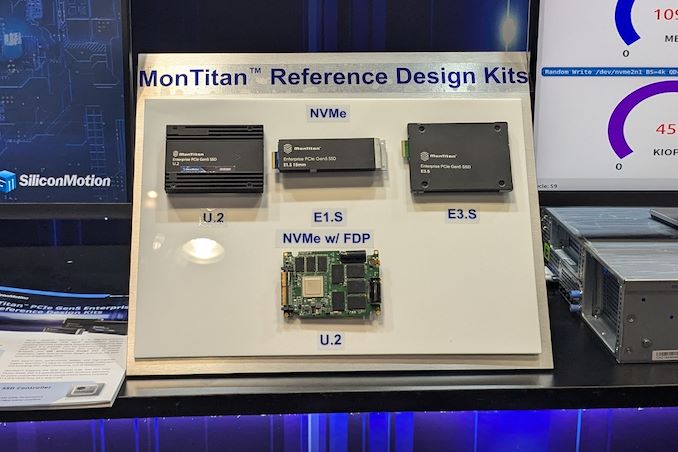
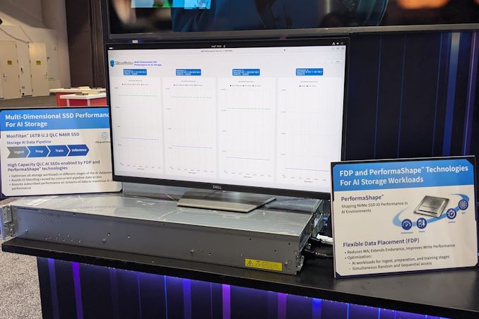
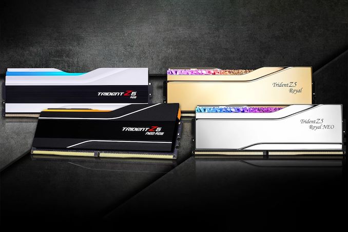
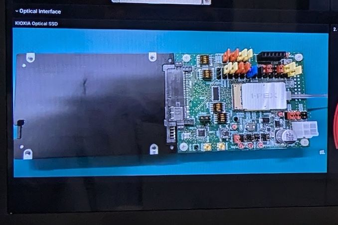
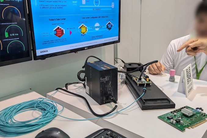
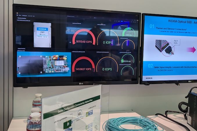




0 Comments