
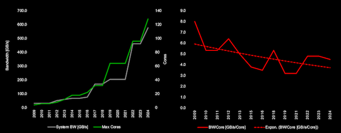
The compute market has always been hungry for memory bandwidth, particularly for high-performance applications in servers and datacenters. In recent years, the explosion in core counts per socket has further accentuated this need. Despite progress in DDR speeds, the available bandwidth per core has unfortunately not seen a corresponding scaling.
The stakeholders in the industry have been attempting to address this by building additional technology on top of existing widely-adopted memory standards. With DDR5, there are currently two technologies attempting to increase the peak bandwidth beyond the official speeds. In late 2022, SK hynix introduced MCR-DIMMs meant for operating with specific Intel server platforms. On the other hand, JEDEC - the standards-setting body - also developed specifications for MR-DIMMs with a similar approach. Both of them build upon existing DDR5 technologies by attempting to combine multiple ranks to improve peak bandwidth and latency.
The MR-DIMM standard is conceptually simple - there are multiple ranks of memory modules operating at standard DDR5 speeds with a data buffer in front. The buffer operates at 2x the speed on the host interface side, allowing for essentially double the transfer rates. The challenges obviously lie in being able to operate the logic in the host memory controller at the higher speed and keeping the power consumption / thermals in check.
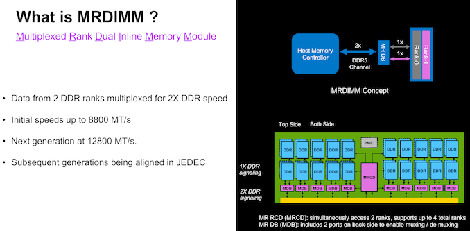
The first version of the JEDEC MR-DIMM standard specifies speeds of 8800 MT/s, with the next generation at 12800 MT/s. JEDEC also has a clear roadmap for this technology, keeping it in sync with the the improvements in the DDR5 standard.
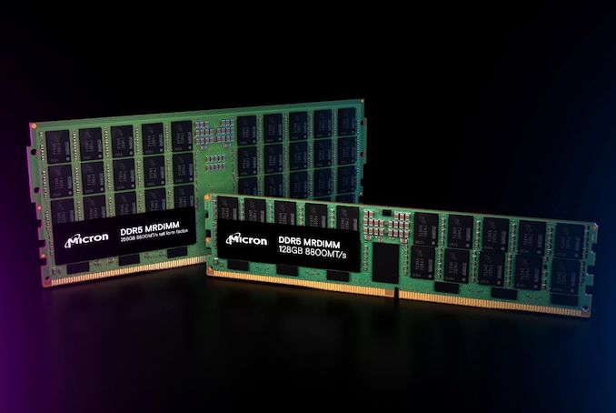
Micron and Intel have been working closely in the last few quarters to bring their former's first-generation MR-DIMM lineup to the market. Intel's Xeon 6 Family with P-Cores (Granite Rapids) is the first platform to bring MR-DIMM support at 8800 MT/s on the host side. Micron's standard-sized MR-DIMMs (suitable for 1U servers) and TFF (tall form-factor) MR-DIMMs (for 2U+ servers) have been qualified for use with the same.
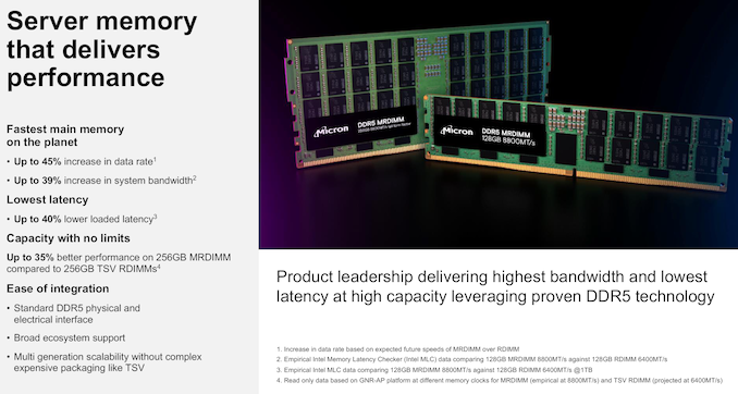
The benefits offered by MR-DIMMs are evident from the JEDEC specifications, allowing for increased data rates and system bandwidth, with improvements in latency. On the capacity side, allowing for additional ranks on the modules has enabled Micron to offer a 256 GB capacity point. It must be noted that some vendors are also using TSV (through-silicon vias) technology to to increase the per-package capacity at standard DDR5 speeds, but this adds additional cost and complexity that are largely absent in the MR-DIMM manufacturing process.
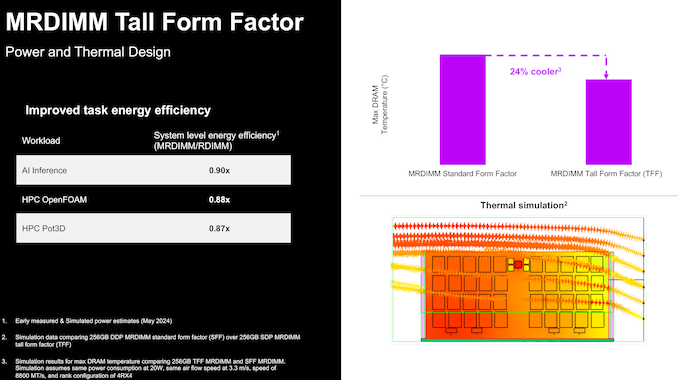
The tall form-factor (TFF) MR-DIMMs have a larger surface area compared to the standard-sized ones. For the same airflow configuration, this allows the DIMM to have a better thermal profile. This provides benefits for energy efficiency as well by reducing the possibility of thermal throttling.
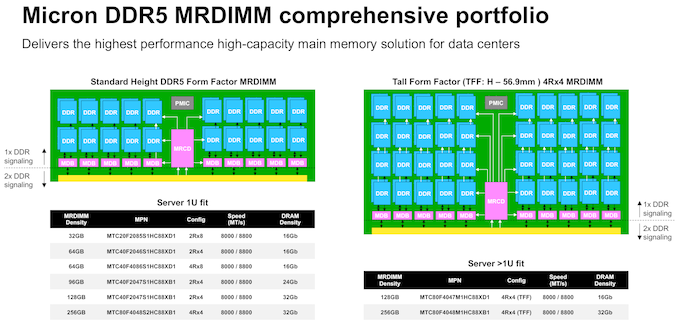
Micron is launching a comprehensive lineup of MR-DIMMs in both standard and tall form-factors today, with multiple DRAM densities and speed options as noted above.
Micron and Intel hosted a media / analyst briefing recently to demonstrate the benefits of MR-DIMMs for Xeon 6 with P-Cores (Granite Rapids). Using a 2P configuration with 96-core Xeon 6 processors, benchmarks for different ... Memory

Standard CPU coolers, while adequate for managing basic thermal loads, often fall short in terms of noise reduction and superior cooling efficiency. This limitation drives advanced users and system builders to seek aftermarket solutions tailored to their specific needs. The high-end aftermarket cooler market is highly competitive, with manufacturers striving to offer products with exceptional performance.
Endorfy, previously known as SilentiumPC, is a Polish manufacturer that has undergone a significant transformation to expand its presence in global markets. The brand is known for delivering high-performance cooling solutions with a strong focus on balancing efficiency and affordability. By rebranding as Endorfy, the company aims to enter premium market segments while continuing to offer reliable, high-quality cooling products.
SilentiumPC became very popular in the value/mainstream segments of the PC market with their products, the spearhead of which probably was the Fera 5 cooler that we reviewed a little over two years ago and had a remarkable value for money. Today’s review places Endorfy’s largest CPU cooler, the Fortis 5 Dual Fan, on our laboratory test bench. The Fortis 5 is the largest CPU air cooler the company currently offers and is significantly more expensive than the Fera 5, yet it still is a single-tower cooler that strives to strike a balance between value, compatibility, and performance.
Cases/Cooling/PSUs

Under the CHIPS & Science Act, the U.S. government provided tens of billions of dollars in grants and loans to the world's leading maker of chips, such as Intel, Samsung, and TSMC, which will significantly expand the country's semiconductor production industry in the coming years. However, most chips are typically tested, assembled, and packaged in Asia, which has left the American supply chain incomplete. Addressing this last gap in the government's domestic chip production plans, these past couple of weeks the U.S. government signed memorandums of understanding worth about $1.5 billion with Amkor and SK hynix to support their efforts to build chip packaging facilities in the U.S.
Amkor plans to build a $2 billion advanced packaging facility near Peoria, Arizona, to test and assemble chips produced by TSMC at its Fab 21 near Phoenix, Arizona. The company signed a MOU that offers $400 million in direct funding and access to $200 million in loans under the CHIPS & Science Act. In addition, the company plans to take advantage of a 25% investment tax credit on eligible capital expenditures.
Set to be strategically positioned near TSMC's upcoming Fab 21 complex in Arizona, Amkor's Peoria facility will occupy 55 acres and, when fully completed, will feature over 500,000 square feet (46,451 square meters) of cleanroom space, more than twice the size of Amkor's advanced packaging site in Vietnam. Although the company has not disclosed the exact capacity or the specific technologies the facility will support, it is expected to cater to a wide range of industries, including automotive, high-performance computing, and mobile technologies. This suggests the new plant will offer diverse packaging solutions, including traditional, 2.5D, and 3D technologies.
Amkor has collaborated extensively with Apple on the vision and initial setup of the Peoria facility, as Apple is slated to be the facility's first and largest customer, marking a significant commitment from the tech giant. This partnership highlights the importance of the new facility in reinforcing the U.S. semiconductor supply chain and positioning Amkor as a key partner for companies relying on TSMC's manufacturing capabilities. The project is expected to generate around 2,000 jobs and is scheduled to begin operations in 2027.
This week SK hynix also signed a preliminary agreement with the U.S. government to receive up to $450 million in direct funding and $500 million in loans to build an advanced memory packaging facility in West Lafayette, Indiana.
The proposed facility is scheduled to begin operations in 2028, which means that it will assemble HBM4 or HBM4E memory. Meanwhile, DRAM devices for high bandwidth memory (HBM) stacks will still be produced in South Korea. Nonetheless, packing finished HBM4/HBM4E in the U.S. and possibly integrating these memory modules with high-end processors is a big deal.
In addition to building its packaging plant, SK hynix plans to collaborate with Purdue University and other local research institutions to advance semiconductor technology and packaging innovations. This partnership is intended to bolster research and development in the region, positioning the facility as a hub for AI technology and skilled employment.
Semiconductors

Kioxia's booth at FMS 2024 was a busy one with multiple technology demonstrations keeping visitors occupied. A walk-through of the BiCS 8 manufacturing process was the first to grab my attention. Kioxia and Western Digital announced the sampling of BiCS 8 in March 2023. We had touched briefly upon its CMOS Bonded Array (CBA) scheme in our coverage of Kioxial's 2Tb QLC NAND device and coverage of Western Digital's 128 TB QLC enterprise SSD proof-of-concept demonstration. At Kioxia's booth, we got more insights.

Traditionally, fabrication of flash chips involved placement of the associate logic circuitry (CMOS process) around the periphery of the flash array. The process then moved on to putting the CMOS under the cell array, but the wafer development process was serialized with the CMOS logic getting fabricated first followed by the cell array on top. However, this has some challenges because the cell array requires a high-temperature processing step to ensure higher reliability that can be detrimental to the health of the CMOS logic. Thanks to recent advancements in wafer bonding techniques, the new CBA process allows the CMOS wafer and cell array wafer to be processed independently in parallel and then pieced together, as shown in the models above.

The BiCS 8 3D NAND incorporates 218 layers, compared to 112 layers in BiCS 5 and 162 layers in BiCS 6. The company decided to skip over BiCS 7 (or, rather, it was probably a short-lived generation meant as an internal test vehicle). The generation retains the four-plane charge trap structure of BiCS 6. In its TLC avatar, it is available as a 1 Tbit device. The QLC version is available in two capacities - 1 Tbit and 2 Tbit.
Kioxia also noted that while the number of layers (218) doesn't compare favorably with the latest layer counts from the competition, its lateral scaling / cell shrinkage has enabled it to be competitive in terms of bit density as well as operating speeds (3200 MT/s). For reference, the latest shipping NAND from Micron - the G9 - has 276 layers with a bit density in TLC mode of 21 Gbit/mm2, and operates at up to 3600 MT/s. However, its 232L NAND operates only up to 2400 MT/s and has a bit density of 14.6 Gbit/mm2.
It must be noted that the CBA hybrid bonding process has advantages over the current processes used by other vendors - including Micron's CMOS under array (CuA) and SK hynix's 4D PUC (periphery-under-chip) developed in the late 2010s. It is expected that other NAND vendors will also move eventually to some variant of the hybrid bonding scheme used by Kioxia.
Storage
Lorem Ipsum is simply dummy text of the printing and typesetting industry. Lorem Ipsum has been the industry's.
Standard CPU coolers, while adequate for managing basic thermal loads, often fall short in terms of noise reduction and superior cooling efficiency. This limitation drives advanced users and system builders to seek aftermarket solutions tailored to their specific needs. The high-end aftermarket cooler market is highly competitive, with manufacturers striving to offer products with exceptional performance.
Endorfy, previously known as SilentiumPC, is a Polish manufacturer that has undergone a significant transformation to expand its presence in global markets. The brand is known for delivering high-performance cooling solutions with a strong focus on balancing efficiency and affordability. By rebranding as Endorfy, the company aims to enter premium market segments while continuing to offer reliable, high-quality cooling products.
SilentiumPC became very popular in the value/mainstream segments of the PC market with their products, the spearhead of which probably was the Fera 5 cooler that we reviewed a little over two years ago and had a remarkable value for money. Today’s review places Endorfy’s largest CPU cooler, the Fortis 5 Dual Fan, on our laboratory test bench. The Fortis 5 is the largest CPU air cooler the company currently offers and is significantly more expensive than the Fera 5, yet it still is a single-tower cooler that strives to strike a balance between value, compatibility, and performance.
Cases/Cooling/PSUs

 is the first platform to bring MR-DIMM support at 8800 MT/s on the host side. Micron's standard-sized MR-DIMMs (suitable for 1U servers) and TFF (tall form-factor) MR-DIMMs (for 2U+ servers) have been qualified for use with the same.</p>
<p align="center"><a href="https://www.anandtech.com/show/21470/micron-mrdimm-lineup-expands-datacenter-dram-portfolio"><img alt="" src="https://images.anandtech.com/doci/21470/micron-mrdimm-lineup-intro_575px.png" /></a></p>
<p>The benefits offered by MR-DIMMs are evident from the JEDEC specifications, allowing for increased data rates and system bandwidth, with improvements in latency. On the capacity side, allowing for additional ranks on the modules has enabled Micron to offer a 256 GB capacity point. It must be noted that some vendors are also using TSV (through-silicon vias) technology to to increase the per-package capacity at standard DDR5 speeds, but this adds additional cost and complexity that are largely absent in the MR-DIMM manufacturing process.</p>
<p align="center"><a href="https://www.anandtech.com/show/21470/micron-mrdimm-lineup-expands-datacenter-dram-portfolio"><img alt="" src="https://images.anandtech.com/doci/21470/micron-mrdimm-tff-benefits_575px.png" /></a></p>
<p>The tall form-factor (TFF) MR-DIMMs have a larger surface area compared to the standard-sized ones. For the same airflow configuration, this allows the DIMM to have a better thermal profile. This provides benefits for energy efficiency as well by reducing the possibility of thermal throttling.</p>
<p align="center"><a href="https://www.anandtech.com/show/21470/micron-mrdimm-lineup-expands-datacenter-dram-portfolio"><img alt="" src="https://images.anandtech.com/doci/21470/micron-mrdimm-lineup-skus_575px.png" /></a></p>
<p>Micron is launching a comprehensive lineup of MR-DIMMs in both standard and tall form-factors today, with multiple DRAM densities and speed options as noted above.</p>
<h3>MRDIMM Benefits - Intel Granite Rapids Gets a Performance Boost</h3>
<p>Micron and Intel hosted a media / analyst briefing recently to demonstrate the benefits of MR-DIMMs for Xeon 6 with P-Cores (Granite Rapids). Using a 2P configuration with 96-core Xeon 6 processors, benchmarks for different ... Memory)
 is the first platform to bring MR-DIMM support at 8800 MT/s on the host side. Micron's standard-sized MR-DIMMs (suitable for 1U servers) and TFF (tall form-factor) MR-DIMMs (for 2U+ servers) have been qualified for use with the same.</p>
<p align="center"><a href="https://www.anandtech.com/show/21470/micron-mrdimm-lineup-expands-datacenter-dram-portfolio"><img alt="" src="https://images.anandtech.com/doci/21470/micron-mrdimm-lineup-intro_575px.png" /></a></p>
<p>The benefits offered by MR-DIMMs are evident from the JEDEC specifications, allowing for increased data rates and system bandwidth, with improvements in latency. On the capacity side, allowing for additional ranks on the modules has enabled Micron to offer a 256 GB capacity point. It must be noted that some vendors are also using TSV (through-silicon vias) technology to to increase the per-package capacity at standard DDR5 speeds, but this adds additional cost and complexity that are largely absent in the MR-DIMM manufacturing process.</p>
<p align="center"><a href="https://www.anandtech.com/show/21470/micron-mrdimm-lineup-expands-datacenter-dram-portfolio"><img alt="" src="https://images.anandtech.com/doci/21470/micron-mrdimm-tff-benefits_575px.png" /></a></p>
<p>The tall form-factor (TFF) MR-DIMMs have a larger surface area compared to the standard-sized ones. For the same airflow configuration, this allows the DIMM to have a better thermal profile. This provides benefits for energy efficiency as well by reducing the possibility of thermal throttling.</p>
<p align="center"><a href="https://www.anandtech.com/show/21470/micron-mrdimm-lineup-expands-datacenter-dram-portfolio"><img alt="" src="https://images.anandtech.com/doci/21470/micron-mrdimm-lineup-skus_575px.png" /></a></p>
<p>Micron is launching a comprehensive lineup of MR-DIMMs in both standard and tall form-factors today, with multiple DRAM densities and speed options as noted above.</p>
<h3>MRDIMM Benefits - Intel Granite Rapids Gets a Performance Boost</h3>
<p>Micron and Intel hosted a media / analyst briefing recently to demonstrate the benefits of MR-DIMMs for Xeon 6 with P-Cores (Granite Rapids). Using a 2P configuration with 96-core Xeon 6 processors, benchmarks for different ... Memory | https://compbuddey.blogspot.com/2024/07/micron-expands-datacenter-dram_29.html)
 is the first platform to bring MR-DIMM support at 8800 MT/s on the host side. Micron's standard-sized MR-DIMMs (suitable for 1U servers) and TFF (tall form-factor) MR-DIMMs (for 2U+ servers) have been qualified for use with the same.</p>
<p align="center"><a href="https://www.anandtech.com/show/21470/micron-mrdimm-lineup-expands-datacenter-dram-portfolio"><img alt="" src="https://images.anandtech.com/doci/21470/micron-mrdimm-lineup-intro_575px.png" /></a></p>
<p>The benefits offered by MR-DIMMs are evident from the JEDEC specifications, allowing for increased data rates and system bandwidth, with improvements in latency. On the capacity side, allowing for additional ranks on the modules has enabled Micron to offer a 256 GB capacity point. It must be noted that some vendors are also using TSV (through-silicon vias) technology to to increase the per-package capacity at standard DDR5 speeds, but this adds additional cost and complexity that are largely absent in the MR-DIMM manufacturing process.</p>
<p align="center"><a href="https://www.anandtech.com/show/21470/micron-mrdimm-lineup-expands-datacenter-dram-portfolio"><img alt="" src="https://images.anandtech.com/doci/21470/micron-mrdimm-tff-benefits_575px.png" /></a></p>
<p>The tall form-factor (TFF) MR-DIMMs have a larger surface area compared to the standard-sized ones. For the same airflow configuration, this allows the DIMM to have a better thermal profile. This provides benefits for energy efficiency as well by reducing the possibility of thermal throttling.</p>
<p align="center"><a href="https://www.anandtech.com/show/21470/micron-mrdimm-lineup-expands-datacenter-dram-portfolio"><img alt="" src="https://images.anandtech.com/doci/21470/micron-mrdimm-lineup-skus_575px.png" /></a></p>
<p>Micron is launching a comprehensive lineup of MR-DIMMs in both standard and tall form-factors today, with multiple DRAM densities and speed options as noted above.</p>
<h3>MRDIMM Benefits - Intel Granite Rapids Gets a Performance Boost</h3>
<p>Micron and Intel hosted a media / analyst briefing recently to demonstrate the benefits of MR-DIMMs for Xeon 6 with P-Cores (Granite Rapids). Using a 2P configuration with 96-core Xeon 6 processors, benchmarks for different ... Memory&body=https://compbuddey.blogspot.com/2024/07/micron-expands-datacenter-dram_29.html)
0 Comments