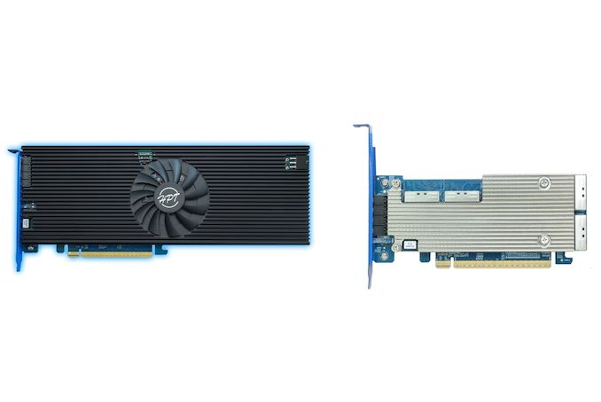

HighPoint Technologies has updated their NVMe switch and RAID solutions with PCIe 5.0, and supporting up to eight NVMe drives. The new HighPoint Rocket 1600 (switch add-in card) and 7600 series (RAID adapters) are the successors to the SSD SSD7500 series adapter cards introduced in 2020. Similar to its predecessors, the new Rocket series cards are also based on a Broadcom PCIe switch (PEX 89048). The Rocket 7600 series runs the RAID stack on the integrated ARM processor (dual-core Cortex A15)
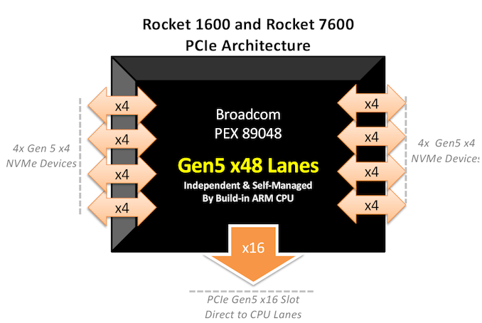
The PEX 89048 supports up to 48 PCIe 5.0 lanes, out of which 16 are dedicated to the host connection in the Rocket adapters. The use of a true PCIe switch means that the product doesn't rely on PCIe lane bifurcation support in the host platform.
HighPoint's Gen 5 stack currently has two products each in the switch and RAID lineups - an add-in card with support for M.2 drives, and a RAID adapter with four 5.0 x8 SFF-TA-1016 (Mini Cool Edge IO or MCIO) connectors for use with backplanes / setups involving U.2 / U.3 / EDSFF drives.
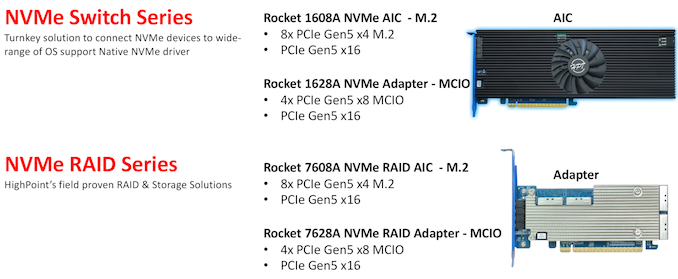
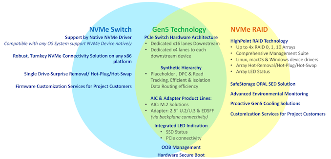
The RAID adapters require HighPoint's drivers (available for Linux, macOS, and Windows), and supports RAID 0, RAID 1, and RAID 10 arrays. On the other hand, the AIC requires no custom drivers. RAID configurations with the AIC will need to be handled by software running on the host OS. On the hardware side, all members of the Rocket series come with an external power connector (as the solution can consume upwards of 75W) and integrate a heatsink. The M.2 version is actively cooled, as the drives are housed within the full-height / full-length cards.
The solution can theoretically support up to 64 GBps of throughput, but real-world performance is limited to around 56 GBps using Gen 5 drives. It must be noted that even Gen 4 drives can take advantage of the new platform and deliver better performance with the new Rocket series compared to the older SSD7500 series.
The cards are shipping now, with pricing ranging from $1500 (add-in card) to $2000 (RAID adapters). HighPoint is not alone in targeting this HEDT / workstation market. Sabrent has been teasing their Apex Gen 5.0 x16 solution involving eight M.2 SSDs for a few months now (involving a Microchip PCIe switch. Until that solution comes to the market, HighPoint appears to be the only game in town for workstation users requiring access to direct-attached storage capable of delivering 50 GBps+ speeds.
SSDs
Standard CPU coolers, while adequate for managing basic thermal loads, often fall short in terms of noise reduction and superior cooling efficiency. This limitation drives advanced users and system builders to seek aftermarket solutions tailored to their specific needs. The high-end aftermarket cooler market is highly competitive, with manufacturers striving to offer products with exceptional performance.
Endorfy, previously known as SilentiumPC, is a Polish manufacturer that has undergone a significant transformation to expand its presence in global markets. The brand is known for delivering high-performance cooling solutions with a strong focus on balancing efficiency and affordability. By rebranding as Endorfy, the company aims to enter premium market segments while continuing to offer reliable, high-quality cooling products.
SilentiumPC became very popular in the value/mainstream segments of the PC market with their products, the spearhead of which probably was the Fera 5 cooler that we reviewed a little over two years ago and had a remarkable value for money. Today’s review places Endorfy’s largest CPU cooler, the Fortis 5 Dual Fan, on our laboratory test bench. The Fortis 5 is the largest CPU air cooler the company currently offers and is significantly more expensive than the Fera 5, yet it still is a single-tower cooler that strives to strike a balance between value, compatibility, and performance.
Cases/Cooling/PSUs

Under the CHIPS & Science Act, the U.S. government provided tens of billions of dollars in grants and loans to the world's leading maker of chips, such as Intel, Samsung, and TSMC, which will significantly expand the country's semiconductor production industry in the coming years. However, most chips are typically tested, assembled, and packaged in Asia, which has left the American supply chain incomplete. Addressing this last gap in the government's domestic chip production plans, these past couple of weeks the U.S. government signed memorandums of understanding worth about $1.5 billion with Amkor and SK hynix to support their efforts to build chip packaging facilities in the U.S.
Amkor plans to build a $2 billion advanced packaging facility near Peoria, Arizona, to test and assemble chips produced by TSMC at its Fab 21 near Phoenix, Arizona. The company signed a MOU that offers $400 million in direct funding and access to $200 million in loans under the CHIPS & Science Act. In addition, the company plans to take advantage of a 25% investment tax credit on eligible capital expenditures.
Set to be strategically positioned near TSMC's upcoming Fab 21 complex in Arizona, Amkor's Peoria facility will occupy 55 acres and, when fully completed, will feature over 500,000 square feet (46,451 square meters) of cleanroom space, more than twice the size of Amkor's advanced packaging site in Vietnam. Although the company has not disclosed the exact capacity or the specific technologies the facility will support, it is expected to cater to a wide range of industries, including automotive, high-performance computing, and mobile technologies. This suggests the new plant will offer diverse packaging solutions, including traditional, 2.5D, and 3D technologies.
Amkor has collaborated extensively with Apple on the vision and initial setup of the Peoria facility, as Apple is slated to be the facility's first and largest customer, marking a significant commitment from the tech giant. This partnership highlights the importance of the new facility in reinforcing the U.S. semiconductor supply chain and positioning Amkor as a key partner for companies relying on TSMC's manufacturing capabilities. The project is expected to generate around 2,000 jobs and is scheduled to begin operations in 2027.
This week SK hynix also signed a preliminary agreement with the U.S. government to receive up to $450 million in direct funding and $500 million in loans to build an advanced memory packaging facility in West Lafayette, Indiana.
The proposed facility is scheduled to begin operations in 2028, which means that it will assemble HBM4 or HBM4E memory. Meanwhile, DRAM devices for high bandwidth memory (HBM) stacks will still be produced in South Korea. Nonetheless, packing finished HBM4/HBM4E in the U.S. and possibly integrating these memory modules with high-end processors is a big deal.
In addition to building its packaging plant, SK hynix plans to collaborate with Purdue University and other local research institutions to advance semiconductor technology and packaging innovations. This partnership is intended to bolster research and development in the region, positioning the facility as a hub for AI technology and skilled employment.
Semiconductors

Kioxia's booth at FMS 2024 was a busy one with multiple technology demonstrations keeping visitors occupied. A walk-through of the BiCS 8 manufacturing process was the first to grab my attention. Kioxia and Western Digital announced the sampling of BiCS 8 in March 2023. We had touched briefly upon its CMOS Bonded Array (CBA) scheme in our coverage of Kioxial's 2Tb QLC NAND device and coverage of Western Digital's 128 TB QLC enterprise SSD proof-of-concept demonstration. At Kioxia's booth, we got more insights.

Traditionally, fabrication of flash chips involved placement of the associate logic circuitry (CMOS process) around the periphery of the flash array. The process then moved on to putting the CMOS under the cell array, but the wafer development process was serialized with the CMOS logic getting fabricated first followed by the cell array on top. However, this has some challenges because the cell array requires a high-temperature processing step to ensure higher reliability that can be detrimental to the health of the CMOS logic. Thanks to recent advancements in wafer bonding techniques, the new CBA process allows the CMOS wafer and cell array wafer to be processed independently in parallel and then pieced together, as shown in the models above.

The BiCS 8 3D NAND incorporates 218 layers, compared to 112 layers in BiCS 5 and 162 layers in BiCS 6. The company decided to skip over BiCS 7 (or, rather, it was probably a short-lived generation meant as an internal test vehicle). The generation retains the four-plane charge trap structure of BiCS 6. In its TLC avatar, it is available as a 1 Tbit device. The QLC version is available in two capacities - 1 Tbit and 2 Tbit.
Kioxia also noted that while the number of layers (218) doesn't compare favorably with the latest layer counts from the competition, its lateral scaling / cell shrinkage has enabled it to be competitive in terms of bit density as well as operating speeds (3200 MT/s). For reference, the latest shipping NAND from Micron - the G9 - has 276 layers with a bit density in TLC mode of 21 Gbit/mm2, and operates at up to 3600 MT/s. However, its 232L NAND operates only up to 2400 MT/s and has a bit density of 14.6 Gbit/mm2.
It must be noted that the CBA hybrid bonding process has advantages over the current processes used by other vendors - including Micron's CMOS under array (CuA) and SK hynix's 4D PUC (periphery-under-chip) developed in the late 2010s. It is expected that other NAND vendors will also move eventually to some variant of the hybrid bonding scheme used by Kioxia.
Storage
Lorem Ipsum is simply dummy text of the printing and typesetting industry. Lorem Ipsum has been the industry's.
Standard CPU coolers, while adequate for managing basic thermal loads, often fall short in terms of noise reduction and superior cooling efficiency. This limitation drives advanced users and system builders to seek aftermarket solutions tailored to their specific needs. The high-end aftermarket cooler market is highly competitive, with manufacturers striving to offer products with exceptional performance.
Endorfy, previously known as SilentiumPC, is a Polish manufacturer that has undergone a significant transformation to expand its presence in global markets. The brand is known for delivering high-performance cooling solutions with a strong focus on balancing efficiency and affordability. By rebranding as Endorfy, the company aims to enter premium market segments while continuing to offer reliable, high-quality cooling products.
SilentiumPC became very popular in the value/mainstream segments of the PC market with their products, the spearhead of which probably was the Fera 5 cooler that we reviewed a little over two years ago and had a remarkable value for money. Today’s review places Endorfy’s largest CPU cooler, the Fortis 5 Dual Fan, on our laboratory test bench. The Fortis 5 is the largest CPU air cooler the company currently offers and is significantly more expensive than the Fera 5, yet it still is a single-tower cooler that strives to strike a balance between value, compatibility, and performance.
Cases/Cooling/PSUs

 and 7600 series (RAID adapters) are the successors to the SSD SSD7500 series adapter cards <a href="https://www.anandtech.com/show/16247">introduced in 2020</a>. Similar to its predecessors, the new Rocket series cards are also based on a Broadcom PCIe switch (PEX 89048). The Rocket 7600 series runs the RAID stack on the integrated ARM processor (dual-core Cortex A15)</p>
<p align="center"><a href="https://www.anandtech.com/show/21486/highpoint-updates-nvme-raid-cards-for-pcie-50-50-gbps-directattached-ssd-storage"><img alt="" src="https://images.anandtech.com/doci/21486/hpt-switch-config_575px.png" /></a></p>
<p>The PEX 89048 supports up to 48 PCIe 5.0 lanes, out of which 16 are dedicated to the host connection in the Rocket adapters. The use of a true PCIe switch means that the product doesn't rely on PCIe lane bifurcation support in the host platform.</p>
<p>HighPoint's Gen 5 stack currently has two products each in the switch and RAID lineups - an add-in card with support for M.2 drives, and a RAID adapter with four 5.0 x8 SFF-TA-1016 (Mini Cool Edge IO or MCIO) connectors for use with backplanes / setups involving U.2 / U.3 / EDSFF drives.</p>
<p align="center"><a href="https://www.anandtech.com/show/21486/highpoint-updates-nvme-raid-cards-for-pcie-50-50-gbps-directattached-ssd-storage"><img alt="" src="https://images.anandtech.com/doci/21486/hpt-prod-stack_575px.png" /></a></p>
<p align="center"><a href="https://www.anandtech.com/show/21486/highpoint-updates-nvme-raid-cards-for-pcie-50-50-gbps-directattached-ssd-storage"><img alt="" src="https://images.anandtech.com/doci/21486/hpt-switch-vs-raid_575px.png" /></a></p>
<p>The RAID adapters require HighPoint's drivers (available for Linux, macOS, and Windows), and supports RAID 0, RAID 1, and RAID 10 arrays. On the other hand, the AIC requires no custom drivers. RAID configurations with the AIC will need to be handled by software running on the host OS. On the hardware side, all members of the Rocket series come with an external power connector (as the solution can consume upwards of 75W) and integrate a heatsink. The M.2 version is actively cooled, as the drives are housed within the full-height / full-length cards.</p>
<p>The solution can theoretically support up to 64 GBps of throughput, but real-world performance is limited to around 56 GBps using Gen 5 drives. It must be noted that even Gen 4 drives can take advantage of the new platform and deliver better performance with the new Rocket series compared to the older SSD7500 series.</p>
<p>The cards are shipping now, with pricing ranging from $1500 (add-in card) to $2000 (RAID adapters). HighPoint is not alone in targeting this HEDT / workstation market. Sabrent has been teasing their Apex Gen 5.0 x16 solution involving eight M.2 SSDs for a few months now (involving a <a href="https://www.microchip.com/en-us/products/interface-and-connectivity/pcie-switches">Microchip PCIe switch</a>. Until that solution comes to the market, HighPoint appears to be the only game in town for workstation users requiring access to direct-attached storage capable of delivering 50 GBps+ speeds.</p>
</p> SSDs)
 and 7600 series (RAID adapters) are the successors to the SSD SSD7500 series adapter cards <a href="https://www.anandtech.com/show/16247">introduced in 2020</a>. Similar to its predecessors, the new Rocket series cards are also based on a Broadcom PCIe switch (PEX 89048). The Rocket 7600 series runs the RAID stack on the integrated ARM processor (dual-core Cortex A15)</p>
<p align="center"><a href="https://www.anandtech.com/show/21486/highpoint-updates-nvme-raid-cards-for-pcie-50-50-gbps-directattached-ssd-storage"><img alt="" src="https://images.anandtech.com/doci/21486/hpt-switch-config_575px.png" /></a></p>
<p>The PEX 89048 supports up to 48 PCIe 5.0 lanes, out of which 16 are dedicated to the host connection in the Rocket adapters. The use of a true PCIe switch means that the product doesn't rely on PCIe lane bifurcation support in the host platform.</p>
<p>HighPoint's Gen 5 stack currently has two products each in the switch and RAID lineups - an add-in card with support for M.2 drives, and a RAID adapter with four 5.0 x8 SFF-TA-1016 (Mini Cool Edge IO or MCIO) connectors for use with backplanes / setups involving U.2 / U.3 / EDSFF drives.</p>
<p align="center"><a href="https://www.anandtech.com/show/21486/highpoint-updates-nvme-raid-cards-for-pcie-50-50-gbps-directattached-ssd-storage"><img alt="" src="https://images.anandtech.com/doci/21486/hpt-prod-stack_575px.png" /></a></p>
<p align="center"><a href="https://www.anandtech.com/show/21486/highpoint-updates-nvme-raid-cards-for-pcie-50-50-gbps-directattached-ssd-storage"><img alt="" src="https://images.anandtech.com/doci/21486/hpt-switch-vs-raid_575px.png" /></a></p>
<p>The RAID adapters require HighPoint's drivers (available for Linux, macOS, and Windows), and supports RAID 0, RAID 1, and RAID 10 arrays. On the other hand, the AIC requires no custom drivers. RAID configurations with the AIC will need to be handled by software running on the host OS. On the hardware side, all members of the Rocket series come with an external power connector (as the solution can consume upwards of 75W) and integrate a heatsink. The M.2 version is actively cooled, as the drives are housed within the full-height / full-length cards.</p>
<p>The solution can theoretically support up to 64 GBps of throughput, but real-world performance is limited to around 56 GBps using Gen 5 drives. It must be noted that even Gen 4 drives can take advantage of the new platform and deliver better performance with the new Rocket series compared to the older SSD7500 series.</p>
<p>The cards are shipping now, with pricing ranging from $1500 (add-in card) to $2000 (RAID adapters). HighPoint is not alone in targeting this HEDT / workstation market. Sabrent has been teasing their Apex Gen 5.0 x16 solution involving eight M.2 SSDs for a few months now (involving a <a href="https://www.microchip.com/en-us/products/interface-and-connectivity/pcie-switches">Microchip PCIe switch</a>. Until that solution comes to the market, HighPoint appears to be the only game in town for workstation users requiring access to direct-attached storage capable of delivering 50 GBps+ speeds.</p>
</p> SSDs | https://compbuddey.blogspot.com/2024/07/highpoint-updates-nvme-raid-cards-for_31.html)
 and 7600 series (RAID adapters) are the successors to the SSD SSD7500 series adapter cards <a href="https://www.anandtech.com/show/16247">introduced in 2020</a>. Similar to its predecessors, the new Rocket series cards are also based on a Broadcom PCIe switch (PEX 89048). The Rocket 7600 series runs the RAID stack on the integrated ARM processor (dual-core Cortex A15)</p>
<p align="center"><a href="https://www.anandtech.com/show/21486/highpoint-updates-nvme-raid-cards-for-pcie-50-50-gbps-directattached-ssd-storage"><img alt="" src="https://images.anandtech.com/doci/21486/hpt-switch-config_575px.png" /></a></p>
<p>The PEX 89048 supports up to 48 PCIe 5.0 lanes, out of which 16 are dedicated to the host connection in the Rocket adapters. The use of a true PCIe switch means that the product doesn't rely on PCIe lane bifurcation support in the host platform.</p>
<p>HighPoint's Gen 5 stack currently has two products each in the switch and RAID lineups - an add-in card with support for M.2 drives, and a RAID adapter with four 5.0 x8 SFF-TA-1016 (Mini Cool Edge IO or MCIO) connectors for use with backplanes / setups involving U.2 / U.3 / EDSFF drives.</p>
<p align="center"><a href="https://www.anandtech.com/show/21486/highpoint-updates-nvme-raid-cards-for-pcie-50-50-gbps-directattached-ssd-storage"><img alt="" src="https://images.anandtech.com/doci/21486/hpt-prod-stack_575px.png" /></a></p>
<p align="center"><a href="https://www.anandtech.com/show/21486/highpoint-updates-nvme-raid-cards-for-pcie-50-50-gbps-directattached-ssd-storage"><img alt="" src="https://images.anandtech.com/doci/21486/hpt-switch-vs-raid_575px.png" /></a></p>
<p>The RAID adapters require HighPoint's drivers (available for Linux, macOS, and Windows), and supports RAID 0, RAID 1, and RAID 10 arrays. On the other hand, the AIC requires no custom drivers. RAID configurations with the AIC will need to be handled by software running on the host OS. On the hardware side, all members of the Rocket series come with an external power connector (as the solution can consume upwards of 75W) and integrate a heatsink. The M.2 version is actively cooled, as the drives are housed within the full-height / full-length cards.</p>
<p>The solution can theoretically support up to 64 GBps of throughput, but real-world performance is limited to around 56 GBps using Gen 5 drives. It must be noted that even Gen 4 drives can take advantage of the new platform and deliver better performance with the new Rocket series compared to the older SSD7500 series.</p>
<p>The cards are shipping now, with pricing ranging from $1500 (add-in card) to $2000 (RAID adapters). HighPoint is not alone in targeting this HEDT / workstation market. Sabrent has been teasing their Apex Gen 5.0 x16 solution involving eight M.2 SSDs for a few months now (involving a <a href="https://www.microchip.com/en-us/products/interface-and-connectivity/pcie-switches">Microchip PCIe switch</a>. Until that solution comes to the market, HighPoint appears to be the only game in town for workstation users requiring access to direct-attached storage capable of delivering 50 GBps+ speeds.</p>
</p> SSDs&body=https://compbuddey.blogspot.com/2024/07/highpoint-updates-nvme-raid-cards-for_31.html)
0 Comments