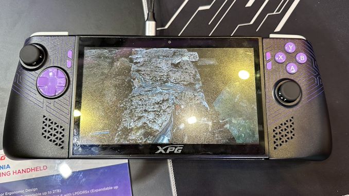

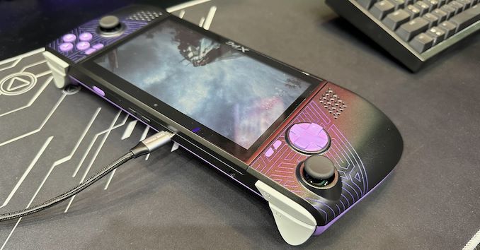
With the rise of the handheld gaming PC market, we've seen PC vendors and their partners toy with a number of tricks and tweaks to improve improve framerates in games, with some of their latest efforts on display at this year's Computex trade show. Perhaps the most interesting find thus far comes from ADATA sub-brand XPG, who is demoing their prototype "Nia" handheld PC, which uses eye tracking and dynamic foveated rendering to further improve their rendering performance.
For those unfamiliar, dynamic foveated rendering is a graphics technique that is sometimes used to boost performance in virtual reality (VR) and augmented reality (AR) applications by taking advantage of how human vision works. Typically, humans can only perceive detailed imagery in the relatively small central area of our vision called the fovea, while our peripheral vision is much less detailed. Dynamic foveated rendering, in turn, exploits this by using real-time eye tracking to determine where the user is looking, and then rendering just that area in high/full resolution, while rendering the peripheral areas in lower resolution. The net result is that only a fraction of the screen is rendered at full detail, which cuts down on the total amount of rendering work required and boosting framerates on performance-limited devices.
As stated before, this technology is sometimes used in high-end AR/VR headsets, where high resolution displays are placed mere inches from one's face. This ends up being an ideal use case for the technique, since at those distances, only a small fraction of the screen is within the fovea.
Using dynamic foveated rendering for a handheld, on the other hand, is a more novel application. All of the same visual principles apply, but the resolutions at play are lower, and the screen is farther from the users' eyes. This makes a handheld device a less ideal use case, at least on paper, as a larger portion of the screen is going to be in the fovea, and thus will need to be rendered at full resolution. None the less, it will be interesting to see how XPG's efforts pan out, and if dynamic foveated rendering is beneficial enough for handheld PCs. As we sometimes see with trade show demos, not everything makes it out of the prototype stage.
According to a press release put out by ADATA ahead of the trade show, the eye tracking technology is being provided by AMD collaborator Eyeware. Notably, their software-based approach runs on top of standard webcams, rather than requiring IR cameras. So the camera hardware itself should be pretty straight-forward.
Foveated rendering aside, XPG is making sure that the Nia won't be a one-trick pony. The handheld's other major claim to fame is its hardware swappability. The prototype handheld not only features a removable M.2-2230 SSD, but the company is also taking advantage of the recently-introduced LPCAMM2 memory module standard to introduce removable DRAM. Via a hatch in the back of the handheld, device owners would be able to swap out LPCAMM2 LPDDR5X modules for higher capacity versions. This would give the handheld an additional degree of future-proofness over current handhelds, which use non-replaceable soldered-down memory.
Rounding out the package, the current prototype is based on an AMD's Zen 4 Phoenix APU, which is used across both of the company's current mobile lines (Ryzen Mobile 7000/8000 and Ryzen Z1). Meanwhile, the unit's display is adjustable, allowing it to be angled away from the body of the handheld.
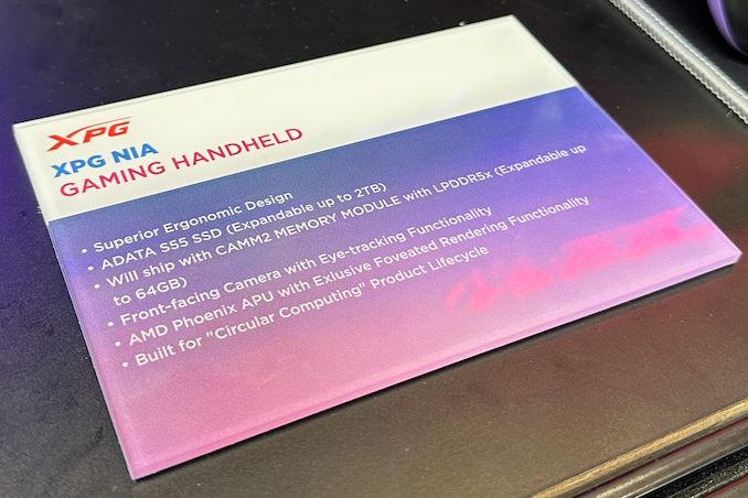
Assuming all goes well with the prototype, XPG aims to release a finished product in 2025.

While the new CAMM and LPCAMM memory modules for laptops have garnered a great deal of attention in recent months, it's not just the mobile side of the PC memory industry that is looking at changes. The desktop memory market is also coming due for some upgrades to further improve DIMM performance, in the form of a new DIMM variety called the Clocked Unbuffered DIMM (CUDIMM). And while this memory isn't in use quite yet, several memory vendors had their initial CUDIMM products on display at this year's Computex trade show, offering a glimpse into the future of desktop memory.
A variation on traditional Unbuffered DIMMs (UDIMMs), Clocked UDIMMs (and Clocked SODIMMs) have been created as another solution to the ongoing signal integrity challenges presented by DDR5 memory. DDR5 allows for rather speedy transfer rates with removable (and easily installed) DIMMs, but further performance increases are running up against the laws of physics when it comes to the electrical challenges of supporting memory on a stick – particularly with so many capacity/performance combinations like we see today. And while those challenges aren't insurmountable, if DDR5 (and eventually, DDR6) are to keep increasing in speed, some changes appear to be needed to produce more electrically robust DIMMs, which is giving rise to the CUDIMM.
Standardized by JEDEC earlier this year as JESD323, CUDIMMs tweak the traditional unbuffered DIMM by adding a clock driver (CKD) to the DIMM itself, with the tiny IC responsible for regenerating the clock signal driving the actual memory chips. By generating a clean clock locally on the DIMM (rather than directly using the clock from the CPU, as is the case today), CUDIMMs are designed to offer improved stability and reliability at high memory speeds, combating the electrical issues that would otherwise cause reliability issues at faster memory speeds. In other words, adding a clock driver is the key to keeping DDR5 operating reliably at high clockspeeds.
All told, JEDEC is proposing that CUDIMMs be used for DDR5-6400 speeds and higher, with the first version of the specification covering speeds up to DDR5-7200. The new DIMMs will also be drop-in compatible with existing platforms (at least on paper), using the same 288-pin connector as today's standard DDR5 UDIMM and allowing for a relatively smooth transition towards higher DDR5 clockspeeds.
Memory

Samsung had quietly launched its BM1743 enterprise QLC SSD last month with a hefty 61.44 TB SKU. At FMS 2024, the company had the even larger 122.88 TB version of that SSD on display, alongside a few recorded benchmarking sessions. Compared to the previous generation, the BM1743 comes with a 4.1x improvement in I/O performance, improvement in data retention, and a 45% improvement in power efficiency for sequential writes.

The 128 TB-class QLC SSD boasts of sequential read speeds of 7.5 GBps and write speeds of 3 GBps. Random reads come in at 1.6 M IOPS, while 16 KB random writes clock in at 45K IOPS. Based on the quoted random write access granularity, it appears that Samsung is using a 16 KB indirection unit (IU) to optimize flash management. This is similar to the strategy adopted by Solidigm with IUs larger than 4K in their high-capacity SSDs.
A recorded benchmark session on the company's PM9D3a 8-channel Gen 5 SSD was also on display.

The SSD family is being promoted as a mainstream option for datacenters, and boasts of sequential reads up to 12 GBps and writes up to 6.8 GBps. Random reads clock in at 2 M IOPS, and random writes at 400 K IOPS.

Available in multiple form-factors up to 32 TB (M.2 tops out at 2 TB), the drive's firmware includes optional support for flexible data placement (FDP) to help address the write amplification aspect.
The PM1753 is the current enterprise SSD flagship in Samsung's lineup. With support for 16 NAND channels and capacities up to 32 TB, this U.2 / E3.S SSD has advertised sequential read and write speeds of 14.8 GBps and 11 GBps respectively. Random reads and writes for 4 KB accesses are listed at 3.4 M and 600 K IOPS.

Samsung claims a 1.7x performance improvement and a 1.7x power efficiency improvement over the previous generation (PM1743), making this TLC SSD suitable for AI servers.
The 9th Gen. V-NAND wafer was also available for viewing, though photography was prohibited. Mass production of this flash memory began in April 2024.
Storage
While the new CAMM and LPCAMM memory modules for laptops have garnered a great deal of attention in recent months, it's not just the mobile side of the PC memory industry that is looking at changes. The desktop memory market is also coming due for some upgrades to further improve DIMM performance, in the form of a new DIMM variety called the Clocked Unbuffered DIMM (CUDIMM). And while this memory isn't in use quite yet, several memory vendors had their initial CUDIMM products on display at this year's Computex trade show, offering a glimpse into the future of desktop memory.
A variation on traditional Unbuffered DIMMs (UDIMMs), Clocked UDIMMs (and Clocked SODIMMs) have been created as another solution to the ongoing signal integrity challenges presented by DDR5 memory. DDR5 allows for rather speedy transfer rates with removable (and easily installed) DIMMs, but further performance increases are running up against the laws of physics when it comes to the electrical challenges of supporting memory on a stick – particularly with so many capacity/performance combinations like we see today. And while those challenges aren't insurmountable, if DDR5 (and eventually, DDR6) are to keep increasing in speed, some changes appear to be needed to produce more electrically robust DIMMs, which is giving rise to the CUDIMM.
Standardized by JEDEC earlier this year as JESD323, CUDIMMs tweak the traditional unbuffered DIMM by adding a clock driver (CKD) to the DIMM itself, with the tiny IC responsible for regenerating the clock signal driving the actual memory chips. By generating a clean clock locally on the DIMM (rather than directly using the clock from the CPU, as is the case today), CUDIMMs are designed to offer improved stability and reliability at high memory speeds, combating the electrical issues that would otherwise cause reliability issues at faster memory speeds. In other words, adding a clock driver is the key to keeping DDR5 operating reliably at high clockspeeds.
All told, JEDEC is proposing that CUDIMMs be used for DDR5-6400 speeds and higher, with the first version of the specification covering speeds up to DDR5-7200. The new DIMMs will also be drop-in compatible with existing platforms (at least on paper), using the same 288-pin connector as today's standard DDR5 UDIMM and allowing for a relatively smooth transition towards higher DDR5 clockspeeds.
Memory
Samsung had quietly launched its BM1743 enterprise QLC SSD last month with a hefty 61.44 TB SKU. At FMS 2024, the company had the even larger 122.88 TB version of that SSD on display, alongside a few recorded benchmarking sessions. Compared to the previous generation, the BM1743 comes with a 4.1x improvement in I/O performance, improvement in data retention, and a 45% improvement in power efficiency for sequential writes.
The 128 TB-class QLC SSD boasts of sequential read speeds of 7.5 GBps and write speeds of 3 GBps. Random reads come in at 1.6 M IOPS, while 16 KB random writes clock in at 45K IOPS. Based on the quoted random write access granularity, it appears that Samsung is using a 16 KB indirection unit (IU) to optimize flash management. This is similar to the strategy adopted by Solidigm with IUs larger than 4K in their high-capacity SSDs.
A recorded benchmark session on the company's PM9D3a 8-channel Gen 5 SSD was also on display.
The SSD family is being promoted as a mainstream option for datacenters, and boasts of sequential reads up to 12 GBps and writes up to 6.8 GBps. Random reads clock in at 2 M IOPS, and random writes at 400 K IOPS.
Available in multiple form-factors up to 32 TB (M.2 tops out at 2 TB), the drive's firmware includes optional support for flexible data placement (FDP) to help address the write amplification aspect.
The PM1753 is the current enterprise SSD flagship in Samsung's lineup. With support for 16 NAND channels and capacities up to 32 TB, this U.2 / E3.S SSD has advertised sequential read and write speeds of 14.8 GBps and 11 GBps respectively. Random reads and writes for 4 KB accesses are listed at 3.4 M and 600 K IOPS.
Samsung claims a 1.7x performance improvement and a 1.7x power efficiency improvement over the previous generation (PM1743), making this TLC SSD suitable for AI servers.
The 9th Gen. V-NAND wafer was also available for viewing, though photography was prohibited. Mass production of this flash memory began in April 2024.
Storage
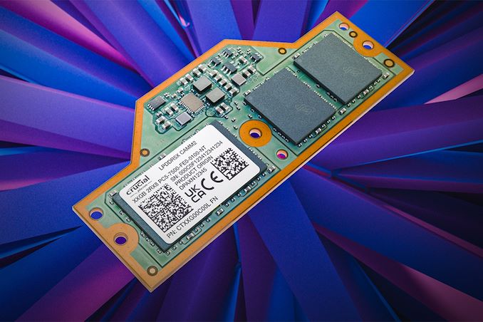
As LPCAMM2 adoption begins, the first retail memory modules are finally starting to hit the retail market, courtesy of Micron. The memory manufacturer has begun selling their LPDDR5X-based LPCAMM2 memory modules under their in-house Crucial brand, making them available on the latter's storefront. Timed to coincide with the release of Lenovo's ThinkPad P1 Gen 7 laptop – the first retail laptop designed to use the memory modules – this marks the de facto start of the eagerly-awaited modular LPDDR5X memory era.
Micron's Low Power Compression Attached Memory Module 2 (LPCAMM2) modules are available in capacities of 32 GB and 64 GB. These are dual-channel modules that feature a 128-bit wide interface, and are based around LPDDR5X memory running at data rates up to 7500 MT/s. This gives a single LPCAMM2 a peak bandwidth of 120 GB/s. Micron is not disclosing the latencies of its LPCAMM2 memory modules, but it says that high data transfer rates of LPDDR5X compensate for the extended timings.
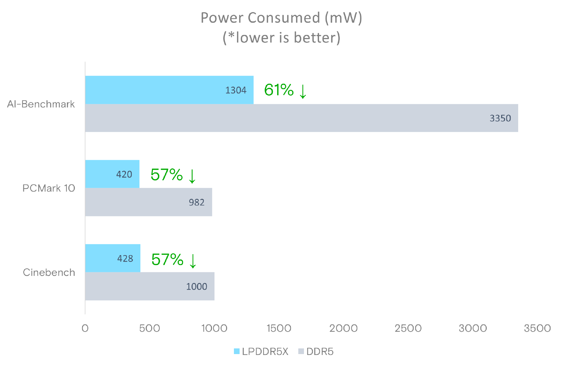
Micron says that LPDDR5X memory offers significantly lower power consumption, with active power per 64-bit bus being 43-58% lower than DDR5 at the same speed, and standby power up to 80% lower. Meanwhile, similar to DDR5 modules, LPCAMM2 modules include a power management IC and voltage regulating circuitry, which provides module manufacturers additional opportunities to reduce power consumption of their products.
Source: Micron LPDDR5X LPCAMM2 Technical Brief
It's worth noting, however, that at least for the first generation of LPCAMM2 modules, system vendors will need to pick between modularity and performance. While soldered-down LPDDR5X memory is available at speeds up to 8533 MT/sec – and with 9600 MT/sec on the horizon – the fastest LPCAMM2 modules planned for this year by both Micron and rival Samsung will be running at 7500 MT/sec. So vendors will have to choose between the flexibility of offering modular LPDDR5X, or the higher bandwidth (and space savings) offered by soldering down their memory.
Micron, for its part, is projecting that 9600 MT/sec LPCAMM2 modules will be available by 2026. Though it's all but certain that faster memory will also be avaialble in the same timeframe.
Micron's Crucial LPDDR5X 32 GB module costs $174.99, whereas a 64 GB module costs $329.99.
Memory
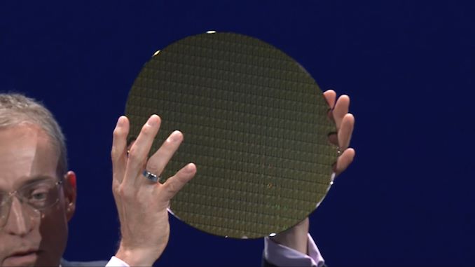
During the Intel keynote hosted by CEO Pat Gelsinger, he gave the world a glimpse into the Intel Client roadmap until 2026. Meteor Lake launched last year on that roadmap, and Lunar Lake, which we dived into yesterday as Intel disclosed technical details about the upcoming platform. Pat also presented a wafer on stage, Panther Lake, and he gave some additional information about Intel's forthcoming Panther Lake platform, which is expected in 2025.
We covered Intel's initial announcement about the Panther Lake platform last year. It is set to be Intel's first client platform using its Intel 18A node. Aside from once again affirming that things are on track for a 2026 launch, Pat Gelsinger, Intel's CEO, also confirmed that they will be powering on the first 18A wafer for Panther Lake as early as next week.
| Intel CPU Architecture Generations | |||||
| Alder/Raptor Lake | Meteor Lake |
Lunar Lake |
Arrow Lake |
Panther Lake |
|
| P-Core Architecture | Golden Cove/ Raptor Cove |
Redwood Cove | Lion Cove | Lion Cove | Cougar Cove? |
| E-Core Architecture | Gracemont | Crestmont | Skymont | Crestmont? | Darkmont? |
| GPU Architecture | Xe-LP | Xe-LPG | Xe2 | Xe2? | ? |
| NPU Architecture | N/A | NPU 3720 | NPU 4 | ? | ? |
| Active Tiles | 1 (Monolithic) | 4 | 2 | 4? | ? |
| Manufacturing Processes | Intel 7 | Intel 4 + TSMC N6 + TSMC N5 | TSMC N3B + TSMC N6 | Intel 20A + More | Intel 18A + ? |
| Segment | Mobile + Desktop | Mobile | LP Mobile | HP Mobile + Desktop | Mobile? |
| Release Date (OEM) | Q4'2021 | Q4'2023 | Q3'2024 | Q4'2024 | 2025 |
One element to consider from last year is that Lunar Lake is built using TSMC, with the Lunar Lake compute tile with Xe2-LPG graphics on TSMC N3B, and the I/O tile on TSMC N6. Pat confirmed on stage that Panther Lake will be on Intel 18A. Still, he didn't confirm whether the chip will be made purely at Intel, or a mix between Intel and external foundries (ala Meteor Lake). Intel has also yet to confirm the CPU cores to be used, but from what our sources tell us, it sounds like it will be the new Cougar Cove and Darkmont cores.
As we head into the second half of 2024 and after Lunar Lake launches, Intel may divulge more information, including the architectural advancements Panther Lake is expected to bring. Until then, we will have to wait and see.
CPUs
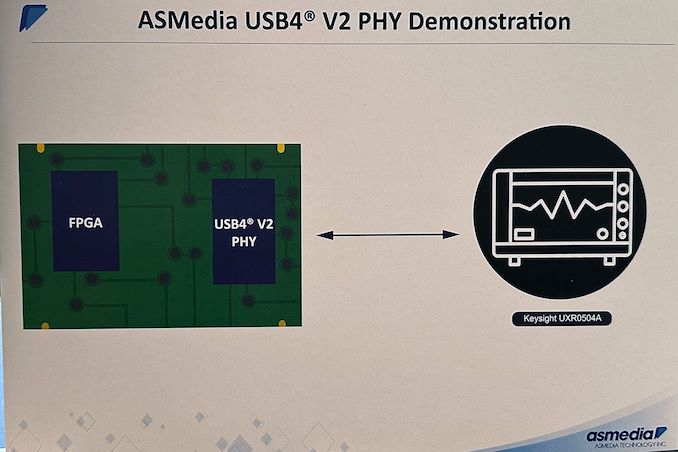
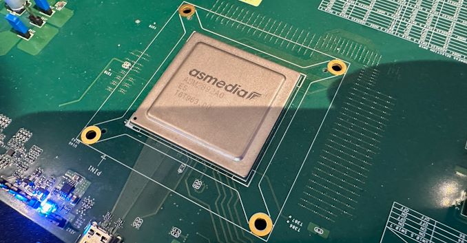
The USB Implementers Forum (USB-IF) introduced USB4 version 2.0 in fall 2022, and it expects systems and devices with the tech to emerge later this year and into next year. These upcoming products will largely rely on Intel's Barlow Ridge controller, a full-featured Thunderbolt 5 controller that goes above and beond the baseline USB4 v2 spec. And though extremely capable, Intel's Thunderbolt controllers are also quite expensive, and Barlow Ridge isn't expected to be any different. Fortunately, for system and device vendors that just need a basic USB4 v2 solution, ASMedia is also working on its own USB4 v2 controller.
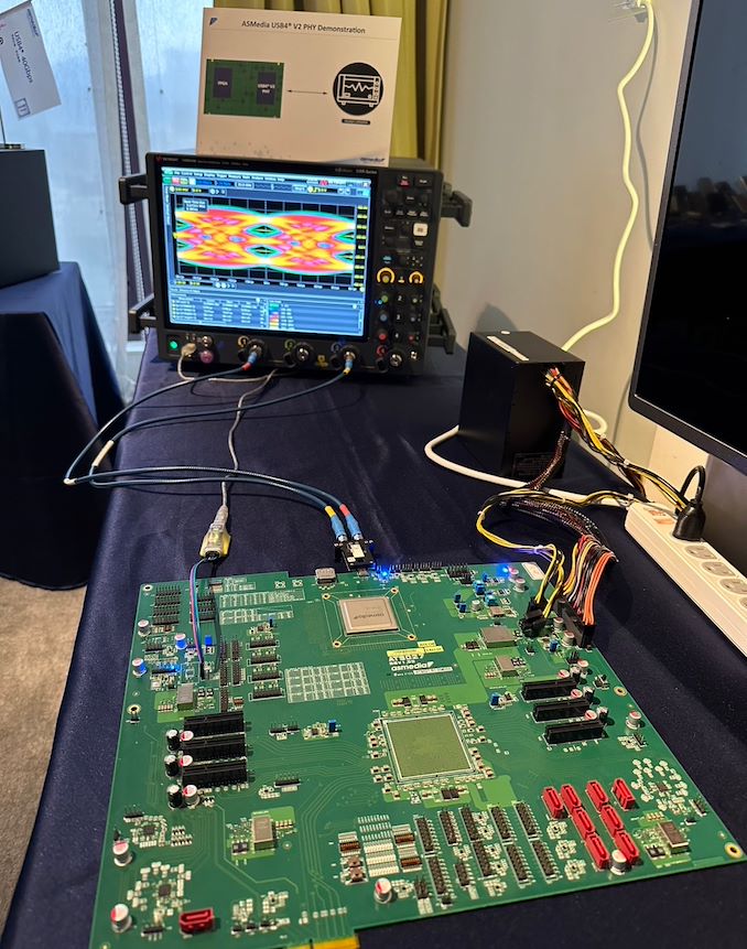
At Computex 2024, ASMedia demonstrated a prototype of its upcoming USB4 v2 physical interface (PHY), which will support USB4 v2's new Gen 4 (160Gbps) data rates and the associated PAM-3 signal encoding. The prototype was implemented using an FPGA, as the company yet has to tape out the completed controller.
Ultimately, the purpose of showing off a FPGA-based PHY at Computex was to allow ASMedia to demonstrate their current PHY design. With the shift to PAM-3 encoding for USB4 v2, ASMedia (and the rest of the USB ecosystem) must develop significantly more complex controllers – and there's no part of that more critical than a solid and reliable PHY design.
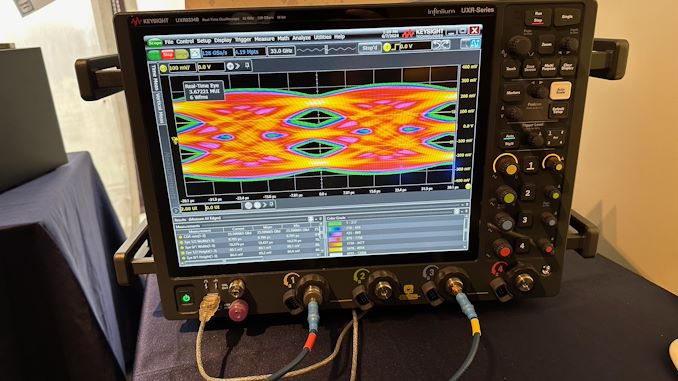
As part of their demonstration, ASMedia had a classic eye diagram display. The eye diagram demoed has a clear opening in the center, which is indicative of good signal integrity, as the larger the eye opening, the less distortion and noise in the signal. The horizontal width of the eye opening represents the time window in which the signal can be sampled correctly, so the relatively narrow horizontal spread of the eye opening suggests that there is minimal jitter, meaning the signal transitions are consistent and predictable. Finally, the vertical height of the eye opening indicates the signal amplitude and the rather tall eye opening suggests a higher signal-to-noise ratio (SNR), meaning that the signal is strong compared to any noise present.
ASMedia itself is one of the major suppliers for discrete USB controllers, so the availability of ASMedia's USB4 v2 chip is crucial for adoption of the standard in general. While Intel will spearhead the industry with their Barlow Ridge Thunderbolt 5/USB4 v2 controller, ASMedia's controller is poised to end up in a far larger range of devices. So the importance of the company's USB4 v2 PHY demo is hard to overstate.
Demos aside, ASMedia is hoping to tape the chip out soon. If all goes well, the company expects their first USB4 v2 controllers to hit the market some time in the second half of 2025.

Lorem Ipsum is simply dummy text of the printing and typesetting industry. Lorem Ipsum has been the industry's.
While the new CAMM and LPCAMM memory modules for laptops have garnered a great deal of attention in recent months, it's not just the mobile side of the PC memory industry that is looking at changes. The desktop memory market is also coming due for some upgrades to further improve DIMM performance, in the form of a new DIMM variety called the Clocked Unbuffered DIMM (CUDIMM). And while this memory isn't in use quite yet, several memory vendors had their initial CUDIMM products on display at this year's Computex trade show, offering a glimpse into the future of desktop memory.
A variation on traditional Unbuffered DIMMs (UDIMMs), Clocked UDIMMs (and Clocked SODIMMs) have been created as another solution to the ongoing signal integrity challenges presented by DDR5 memory. DDR5 allows for rather speedy transfer rates with removable (and easily installed) DIMMs, but further performance increases are running up against the laws of physics when it comes to the electrical challenges of supporting memory on a stick – particularly with so many capacity/performance combinations like we see today. And while those challenges aren't insurmountable, if DDR5 (and eventually, DDR6) are to keep increasing in speed, some changes appear to be needed to produce more electrically robust DIMMs, which is giving rise to the CUDIMM.
Standardized by JEDEC earlier this year as JESD323, CUDIMMs tweak the traditional unbuffered DIMM by adding a clock driver (CKD) to the DIMM itself, with the tiny IC responsible for regenerating the clock signal driving the actual memory chips. By generating a clean clock locally on the DIMM (rather than directly using the clock from the CPU, as is the case today), CUDIMMs are designed to offer improved stability and reliability at high memory speeds, combating the electrical issues that would otherwise cause reliability issues at faster memory speeds. In other words, adding a clock driver is the key to keeping DDR5 operating reliably at high clockspeeds.
All told, JEDEC is proposing that CUDIMMs be used for DDR5-6400 speeds and higher, with the first version of the specification covering speeds up to DDR5-7200. The new DIMMs will also be drop-in compatible with existing platforms (at least on paper), using the same 288-pin connector as today's standard DDR5 UDIMM and allowing for a relatively smooth transition towards higher DDR5 clockspeeds.
Memory
Samsung had quietly launched its BM1743 enterprise QLC SSD last month with a hefty 61.44 TB SKU. At FMS 2024, the company had the even larger 122.88 TB version of that SSD on display, alongside a few recorded benchmarking sessions. Compared to the previous generation, the BM1743 comes with a 4.1x improvement in I/O performance, improvement in data retention, and a 45% improvement in power efficiency for sequential writes.
The 128 TB-class QLC SSD boasts of sequential read speeds of 7.5 GBps and write speeds of 3 GBps. Random reads come in at 1.6 M IOPS, while 16 KB random writes clock in at 45K IOPS. Based on the quoted random write access granularity, it appears that Samsung is using a 16 KB indirection unit (IU) to optimize flash management. This is similar to the strategy adopted by Solidigm with IUs larger than 4K in their high-capacity SSDs.
A recorded benchmark session on the company's PM9D3a 8-channel Gen 5 SSD was also on display.
The SSD family is being promoted as a mainstream option for datacenters, and boasts of sequential reads up to 12 GBps and writes up to 6.8 GBps. Random reads clock in at 2 M IOPS, and random writes at 400 K IOPS.
Available in multiple form-factors up to 32 TB (M.2 tops out at 2 TB), the drive's firmware includes optional support for flexible data placement (FDP) to help address the write amplification aspect.
The PM1753 is the current enterprise SSD flagship in Samsung's lineup. With support for 16 NAND channels and capacities up to 32 TB, this U.2 / E3.S SSD has advertised sequential read and write speeds of 14.8 GBps and 11 GBps respectively. Random reads and writes for 4 KB accesses are listed at 3.4 M and 600 K IOPS.
Samsung claims a 1.7x performance improvement and a 1.7x power efficiency improvement over the previous generation (PM1743), making this TLC SSD suitable for AI servers.
The 9th Gen. V-NAND wafer was also available for viewing, though photography was prohibited. Mass production of this flash memory began in April 2024.
Storage


 and augmented reality (AR) applications by taking advantage of how human vision works. Typically, humans can only perceive detailed imagery in the relatively small central area of our vision called the fovea, while our peripheral vision is much less detailed. Dynamic foveated rendering, in turn, exploits this by using real-time eye tracking to determine where the user is looking, and then rendering just that area in high/full resolution, while rendering the peripheral areas in lower resolution. The net result is that only a fraction of the screen is rendered at full detail, which cuts down on the total amount of rendering work required and boosting framerates on performance-limited devices.</p>
<p style="text-align: center;"><a href="https://www.anandtech.com/show/21432/xpg-demos-nia-handheld-gaming-pc-foveated-rendering-swappable-dram"><img alt="" src="https://images.anandtech.com/doci/21432/IMG_9819_575px.jpg" /></a></p>
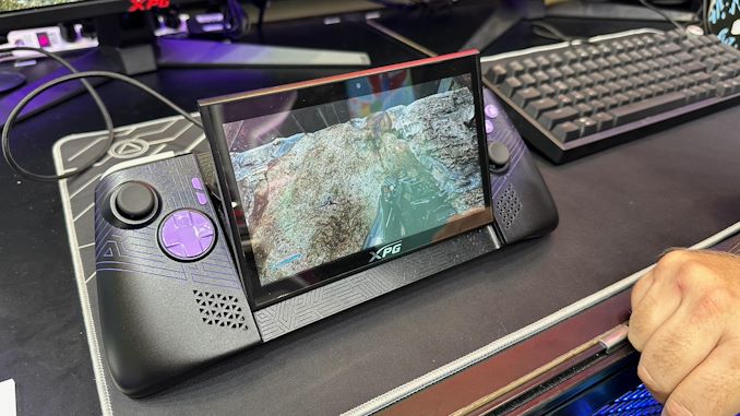
<p>As stated before, this technology is sometimes used in high-end AR/VR headsets, where high resolution displays are placed mere inches from one's face. This ends up being an ideal use case for the technique, since at those distances, only a small fraction of the screen is within the fovea.</p>
<p>Using dynamic foveated rendering for a handheld, on the other hand, is a more novel application. All of the same visual principles apply, but the resolutions at play are lower, and the screen is farther from the users' eyes. This makes a handheld device a less ideal use case, at least on paper, as a larger portion of the screen is going to be in the fovea, and thus will need to be rendered at full resolution. None the less, it will be interesting to see how XPG's efforts pan out, and if dynamic foveated rendering is beneficial enough for handheld PCs. As we sometimes see with trade show demos, not everything makes it out of the prototype stage.</p>
<p align="center"><a href="https://www.anandtech.com/show/21432/xpg-demos-nia-handheld-gaming-pc-foveated-rendering-swappable-dram"><img alt="" src="https://images.anandtech.com/doci/21432/IMG_9823_575px.jpg" /></a></p>
<p>According to a press release put out by ADATA ahead of the trade show, the eye tracking technology is being provided by AMD collaborator <a href="https://beam.eyeware.tech/">Eyeware</a>. Notably, their software-based approach runs on top of standard webcams, rather than requiring IR cameras. So the camera hardware itself should be pretty straight-forward.</p>
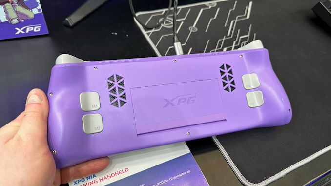
<p>Foveated rendering aside, XPG is making sure that the Nia won't be a one-trick pony. The handheld's other major claim to fame is its hardware swappability. The prototype handheld not only features a removable M.2-2230 SSD, but the company is also taking advantage of the recently-introduced LPCAMM2 memory module standard to introduce removable DRAM. Via a hatch in the back of the handheld, device owners would be able to swap out LPCAMM2 LPDDR5X modules for higher capacity versions. This would give the handheld an additional degree of future-proofness over current handhelds, which use non-replaceable soldered-down memory.</p>
<p>Rounding out the package, the current prototype is based on an AMD's Zen 4 Phoenix APU, which is used across both of the company's current mobile lines (Ryzen Mobile 7000/8000 and Ryzen Z1). Meanwhile, the unit's display is adjustable, allowing it to be angled away from the body of the handheld.</p>
<p align="center"><a href="https://www.anandtech.com/show/21432/xpg-demos-nia-handheld-gaming-pc-foveated-rendering-swappable-dram"><img alt="" src="https://images.anandtech.com/doci/21432/IMG_9818-678-specs_575px.jpg" /></a></p>
<p>Assuming all goes well with the prototype, XPG aims to release a finished product in 2025.</p>
<p style="text-align: center;"><a href="https://www.anandtech.com/show/21432/xpg-demos-nia-handheld-gaming-pc-foveated-rendering-swappable-dram"><img alt="" src="https://images.anandtech.com/doci/21432/IMG_9824_575px.jpg" /></a></p>
</p> ADATA)
 and augmented reality (AR) applications by taking advantage of how human vision works. Typically, humans can only perceive detailed imagery in the relatively small central area of our vision called the fovea, while our peripheral vision is much less detailed. Dynamic foveated rendering, in turn, exploits this by using real-time eye tracking to determine where the user is looking, and then rendering just that area in high/full resolution, while rendering the peripheral areas in lower resolution. The net result is that only a fraction of the screen is rendered at full detail, which cuts down on the total amount of rendering work required and boosting framerates on performance-limited devices.</p>
<p style="text-align: center;"><a href="https://www.anandtech.com/show/21432/xpg-demos-nia-handheld-gaming-pc-foveated-rendering-swappable-dram"><img alt="" src="https://images.anandtech.com/doci/21432/IMG_9819_575px.jpg" /></a></p>
<p>As stated before, this technology is sometimes used in high-end AR/VR headsets, where high resolution displays are placed mere inches from one's face. This ends up being an ideal use case for the technique, since at those distances, only a small fraction of the screen is within the fovea.</p>
<p>Using dynamic foveated rendering for a handheld, on the other hand, is a more novel application. All of the same visual principles apply, but the resolutions at play are lower, and the screen is farther from the users' eyes. This makes a handheld device a less ideal use case, at least on paper, as a larger portion of the screen is going to be in the fovea, and thus will need to be rendered at full resolution. None the less, it will be interesting to see how XPG's efforts pan out, and if dynamic foveated rendering is beneficial enough for handheld PCs. As we sometimes see with trade show demos, not everything makes it out of the prototype stage.</p>
<p align="center"><a href="https://www.anandtech.com/show/21432/xpg-demos-nia-handheld-gaming-pc-foveated-rendering-swappable-dram"><img alt="" src="https://images.anandtech.com/doci/21432/IMG_9823_575px.jpg" /></a></p>
<p>According to a press release put out by ADATA ahead of the trade show, the eye tracking technology is being provided by AMD collaborator <a href="https://beam.eyeware.tech/">Eyeware</a>. Notably, their software-based approach runs on top of standard webcams, rather than requiring IR cameras. So the camera hardware itself should be pretty straight-forward.</p>
<p>Foveated rendering aside, XPG is making sure that the Nia won't be a one-trick pony. The handheld's other major claim to fame is its hardware swappability. The prototype handheld not only features a removable M.2-2230 SSD, but the company is also taking advantage of the recently-introduced LPCAMM2 memory module standard to introduce removable DRAM. Via a hatch in the back of the handheld, device owners would be able to swap out LPCAMM2 LPDDR5X modules for higher capacity versions. This would give the handheld an additional degree of future-proofness over current handhelds, which use non-replaceable soldered-down memory.</p>
<p>Rounding out the package, the current prototype is based on an AMD's Zen 4 Phoenix APU, which is used across both of the company's current mobile lines (Ryzen Mobile 7000/8000 and Ryzen Z1). Meanwhile, the unit's display is adjustable, allowing it to be angled away from the body of the handheld.</p>
<p align="center"><a href="https://www.anandtech.com/show/21432/xpg-demos-nia-handheld-gaming-pc-foveated-rendering-swappable-dram"><img alt="" src="https://images.anandtech.com/doci/21432/IMG_9818-678-specs_575px.jpg" /></a></p>
<p>Assuming all goes well with the prototype, XPG aims to release a finished product in 2025.</p>
<p style="text-align: center;"><a href="https://www.anandtech.com/show/21432/xpg-demos-nia-handheld-gaming-pc-foveated-rendering-swappable-dram"><img alt="" src="https://images.anandtech.com/doci/21432/IMG_9824_575px.jpg" /></a></p>
</p> ADATA | https://compbuddey.blogspot.com/2024/06/xpg-demos-nia-handheld-gaming-pc-with_70.html)
 and augmented reality (AR) applications by taking advantage of how human vision works. Typically, humans can only perceive detailed imagery in the relatively small central area of our vision called the fovea, while our peripheral vision is much less detailed. Dynamic foveated rendering, in turn, exploits this by using real-time eye tracking to determine where the user is looking, and then rendering just that area in high/full resolution, while rendering the peripheral areas in lower resolution. The net result is that only a fraction of the screen is rendered at full detail, which cuts down on the total amount of rendering work required and boosting framerates on performance-limited devices.</p>
<p style="text-align: center;"><a href="https://www.anandtech.com/show/21432/xpg-demos-nia-handheld-gaming-pc-foveated-rendering-swappable-dram"><img alt="" src="https://images.anandtech.com/doci/21432/IMG_9819_575px.jpg" /></a></p>
<p>As stated before, this technology is sometimes used in high-end AR/VR headsets, where high resolution displays are placed mere inches from one's face. This ends up being an ideal use case for the technique, since at those distances, only a small fraction of the screen is within the fovea.</p>
<p>Using dynamic foveated rendering for a handheld, on the other hand, is a more novel application. All of the same visual principles apply, but the resolutions at play are lower, and the screen is farther from the users' eyes. This makes a handheld device a less ideal use case, at least on paper, as a larger portion of the screen is going to be in the fovea, and thus will need to be rendered at full resolution. None the less, it will be interesting to see how XPG's efforts pan out, and if dynamic foveated rendering is beneficial enough for handheld PCs. As we sometimes see with trade show demos, not everything makes it out of the prototype stage.</p>
<p align="center"><a href="https://www.anandtech.com/show/21432/xpg-demos-nia-handheld-gaming-pc-foveated-rendering-swappable-dram"><img alt="" src="https://images.anandtech.com/doci/21432/IMG_9823_575px.jpg" /></a></p>
<p>According to a press release put out by ADATA ahead of the trade show, the eye tracking technology is being provided by AMD collaborator <a href="https://beam.eyeware.tech/">Eyeware</a>. Notably, their software-based approach runs on top of standard webcams, rather than requiring IR cameras. So the camera hardware itself should be pretty straight-forward.</p>
<p>Foveated rendering aside, XPG is making sure that the Nia won't be a one-trick pony. The handheld's other major claim to fame is its hardware swappability. The prototype handheld not only features a removable M.2-2230 SSD, but the company is also taking advantage of the recently-introduced LPCAMM2 memory module standard to introduce removable DRAM. Via a hatch in the back of the handheld, device owners would be able to swap out LPCAMM2 LPDDR5X modules for higher capacity versions. This would give the handheld an additional degree of future-proofness over current handhelds, which use non-replaceable soldered-down memory.</p>
<p>Rounding out the package, the current prototype is based on an AMD's Zen 4 Phoenix APU, which is used across both of the company's current mobile lines (Ryzen Mobile 7000/8000 and Ryzen Z1). Meanwhile, the unit's display is adjustable, allowing it to be angled away from the body of the handheld.</p>
<p align="center"><a href="https://www.anandtech.com/show/21432/xpg-demos-nia-handheld-gaming-pc-foveated-rendering-swappable-dram"><img alt="" src="https://images.anandtech.com/doci/21432/IMG_9818-678-specs_575px.jpg" /></a></p>
<p>Assuming all goes well with the prototype, XPG aims to release a finished product in 2025.</p>
<p style="text-align: center;"><a href="https://www.anandtech.com/show/21432/xpg-demos-nia-handheld-gaming-pc-foveated-rendering-swappable-dram"><img alt="" src="https://images.anandtech.com/doci/21432/IMG_9824_575px.jpg" /></a></p>
</p> ADATA&body=https://compbuddey.blogspot.com/2024/06/xpg-demos-nia-handheld-gaming-pc-with_70.html)
0 Comments