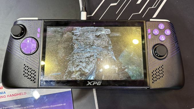

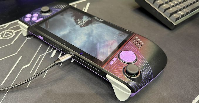
With the rise of the handheld gaming PC market, we've seen PC vendors and their partners toy with a number of tricks and tweaks to improve improve framerates in games, with some of their latest efforts on display at this year's Computex trade show. Perhaps the most interesting find thus far comes from ADATA sub-brand XPG, who is demoing their prototype "Nia" handheld PC, which uses eye tracking and dynamic foveated rendering to further improve their rendering performance.
For those unfamiliar, dynamic foveated rendering is a graphics technique that is sometimes used to boost performance in virtual reality (VR) and augmented reality (AR) applications by taking advantage of how human vision works. Typically, humans can only perceive detailed imagery in the relatively small central area of our vision called the fovea, while our peripheral vision is much less detailed. Dynamic foveated rendering, in turn, exploits this by using real-time eye tracking to determine where the user is looking, and then rendering just that area in high/full resolution, while rendering the peripheral areas in lower resolution. The net result is that only a fraction of the screen is rendered at full detail, which cuts down on the total amount of rendering work required and boosting framerates on performance-limited devices.
As stated before, this technology is sometimes used in high-end AR/VR headsets, where high resolution displays are placed mere inches from one's face. This ends up being an ideal use case for the technique, since at those distances, only a small fraction of the screen is within the fovea.
Using dynamic foveated rendering for a handheld, on the other hand, is a more novel application. All of the same visual principles apply, but the resolutions at play are lower, and the screen is farther from the users' eyes. This makes a handheld device a less ideal use case, at least on paper, as a larger portion of the screen is going to be in the fovea, and thus will need to be rendered at full resolution. None the less, it will be interesting to see how XPG's efforts pan out, and if dynamic foveated rendering is beneficial enough for handheld PCs. As we sometimes see with trade show demos, not everything makes it out of the prototype stage.
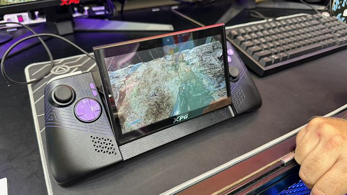
According to a press release put out by ADATA ahead of the trade show, the eye tracking technology is being provided by AMD collaborator Eyeware. Notably, their software-based approach runs on top of standard webcams, rather than requiring IR cameras. So the camera hardware itself should be pretty straight-forward.
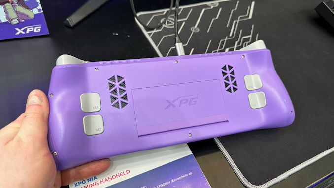
Foveated rendering aside, XPG is making sure that the Nia won't be a one-trick pony. The handheld's other major claim to fame is its hardware swappability. The prototype handheld not only features a removable M.2-2230 SSD, but the company is also taking advantage of the recently-introduced LPCAMM2 memory module standard to introduce removable DRAM. Via a hatch in the back of the handheld, device owners would be able to swap out LPCAMM2 LPDDR5X modules for higher capacity versions. This would give the handheld an additional degree of future-proofness over current handhelds, which use non-replaceable soldered-down memory.
Rounding out the package, the current prototype is based on an AMD's Zen 4 Phoenix APU, which is used across both of the company's current mobile lines (Ryzen Mobile 7000/8000 and Ryzen Z1). Meanwhile, the unit's display is adjustable, allowing it to be angled away from the body of the handheld.
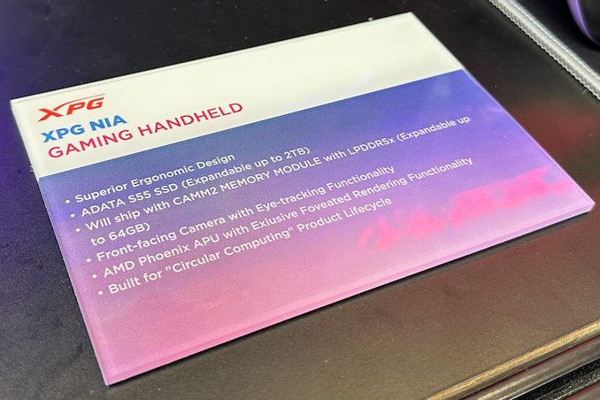
Assuming all goes well with the prototype, XPG aims to release a finished product in 2025.


Kioxia's booth at FMS 2024 was a busy one with multiple technology demonstrations keeping visitors occupied. A walk-through of the BiCS 8 manufacturing process was the first to grab my attention. Kioxia and Western Digital announced the sampling of BiCS 8 in March 2023. We had touched briefly upon its CMOS Bonded Array (CBA) scheme in our coverage of Kioxial's 2Tb QLC NAND device and coverage of Western Digital's 128 TB QLC enterprise SSD proof-of-concept demonstration. At Kioxia's booth, we got more insights.

Traditionally, fabrication of flash chips involved placement of the associate logic circuitry (CMOS process) around the periphery of the flash array. The process then moved on to putting the CMOS under the cell array, but the wafer development process was serialized with the CMOS logic getting fabricated first followed by the cell array on top. However, this has some challenges because the cell array requires a high-temperature processing step to ensure higher reliability that can be detrimental to the health of the CMOS logic. Thanks to recent advancements in wafer bonding techniques, the new CBA process allows the CMOS wafer and cell array wafer to be processed independently in parallel and then pieced together, as shown in the models above.

The BiCS 8 3D NAND incorporates 218 layers, compared to 112 layers in BiCS 5 and 162 layers in BiCS 6. The company decided to skip over BiCS 7 (or, rather, it was probably a short-lived generation meant as an internal test vehicle). The generation retains the four-plane charge trap structure of BiCS 6. In its TLC avatar, it is available as a 1 Tbit device. The QLC version is available in two capacities - 1 Tbit and 2 Tbit.
Kioxia also noted that while the number of layers (218) doesn't compare favorably with the latest layer counts from the competition, its lateral scaling / cell shrinkage has enabled it to be competitive in terms of bit density as well as operating speeds (3200 MT/s). For reference, the latest shipping NAND from Micron - the G9 - has 276 layers with a bit density in TLC mode of 21 Gbit/mm2, and operates at up to 3600 MT/s. However, its 232L NAND operates only up to 2400 MT/s and has a bit density of 14.6 Gbit/mm2.
It must be noted that the CBA hybrid bonding process has advantages over the current processes used by other vendors - including Micron's CMOS under array (CuA) and SK hynix's 4D PUC (periphery-under-chip) developed in the late 2010s. It is expected that other NAND vendors will also move eventually to some variant of the hybrid bonding scheme used by Kioxia.
Storage
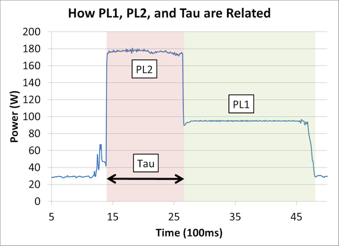
Across the internet, from online forums such as Reddit to various other tech media outlets, there's a lot of furor around reports of Intel's top-end 14th and 13th Gen K series of processors running into stability issues. As Intel's flagship chips, these parts come aggressively clocked in order to maximize performance through various implementations of boost and turbo, leaving them running close to their limits out of the box. But with high-end motherboards further goosing these chips to wring even more performance out of them, it would seem that the Intel desktop ecosystem has finally reached a tipping point where all of these efforts to boost performance have pushed these flagship chips to unstable conditions. To that end, Intel has released new gudiance to its consumer motherboard partners, strongly encouraging them to actually implment Intel's stock power settings, and to use those baseline settings as their out-of-the-box default.
While the underlying conditions are nothing new – we've published stories time and time again about motherboard features such as multi-core enhancement (MCE) and raised power consumption limits that seek to maximize how hard and how long systems are able to turbo boost – the issue has finally come to a head in the last couple of months thanks to accumulating reports of system instability with Intel's 13900K and 14900K processors. These instability problems are eventually solved by either tamping down on these motherboard performance-boosting features – bringing the chips back down to something closer to Intel's official operating parameters – or downclocking the chips entirely.
Intel first began publicly investigating the matter on the 27th of February, when Intel's Communications Manager, Thomas Hannaford, posted a thread on Intel's Community Product Support Forms titled "Regarding Reports of 13th/14th Gen Unlocked Desktop Users Experiencing Stability Issues". In this thread, Thomas Hannaford said, "Intel is aware of reports regarding Intel Core 13th and 14th Gen unlocked desktop processors experiencing issues with certain workloads. We're engaged with our partners and are conducting analysis of the reported issues. If you are experiencing these issues, please reach out to Intel Customer Support for further assistance in the interim."
Since that post went up, additional reports have been circulating about instability issues across various online forums and message boards. The underlying culprit has been theorized to be motherboards implementing an array of strategies to improve chip performance, including aggressive multi-core enhancement settings, "unlimited" PL2 turbo, and reduced load line calibration settings. At no point do any of these settings overclock a CPU and push it to a higher clockspeed than it's validated for, but these settings do everything possible to keep a chip at the highest clockspeed possible at all times – and in the process seem to have gone a step too far.
From "Why Intel Processors Draw More Power Than Expected: TDP and Turbo Explained"
We wrote a piece initially covering multi-core enhancement in 2012, detailing how motherboard manufacturers try to stay competitive with each other and leverage any headroom within the silicon to output the highest performance levels. And more recently, we've talked about how desktop systems with Intel chips are now regularly exceeding their rated TDPs – sometimes by extreme amounts – as motherboard vendors continue to push them to run as hard as possible for the best performance.
But things have changed since 2012. At the time, this wasn't so much of an issue, as overclocking was actually very favorable to increasing the performance of processors. But in 2024 with chips such as the Intel Core i9-14900K, we have CPUs shipping with a maximum turbo clock speed of 6.0 GHz and a peak power consumption of over 400 Watts, figures that were only a pipe dream a decade ago.
Jumping to the present time, over the weekend Intel released a statement about the matter to its partners, outlining their investigation so far and their sug... CPUs
Kioxia's booth at FMS 2024 was a busy one with multiple technology demonstrations keeping visitors occupied. A walk-through of the BiCS 8 manufacturing process was the first to grab my attention. Kioxia and Western Digital announced the sampling of BiCS 8 in March 2023. We had touched briefly upon its CMOS Bonded Array (CBA) scheme in our coverage of Kioxial's 2Tb QLC NAND device and coverage of Western Digital's 128 TB QLC enterprise SSD proof-of-concept demonstration. At Kioxia's booth, we got more insights.
Traditionally, fabrication of flash chips involved placement of the associate logic circuitry (CMOS process) around the periphery of the flash array. The process then moved on to putting the CMOS under the cell array, but the wafer development process was serialized with the CMOS logic getting fabricated first followed by the cell array on top. However, this has some challenges because the cell array requires a high-temperature processing step to ensure higher reliability that can be detrimental to the health of the CMOS logic. Thanks to recent advancements in wafer bonding techniques, the new CBA process allows the CMOS wafer and cell array wafer to be processed independently in parallel and then pieced together, as shown in the models above.
The BiCS 8 3D NAND incorporates 218 layers, compared to 112 layers in BiCS 5 and 162 layers in BiCS 6. The company decided to skip over BiCS 7 (or, rather, it was probably a short-lived generation meant as an internal test vehicle). The generation retains the four-plane charge trap structure of BiCS 6. In its TLC avatar, it is available as a 1 Tbit device. The QLC version is available in two capacities - 1 Tbit and 2 Tbit.
Kioxia also noted that while the number of layers (218) doesn't compare favorably with the latest layer counts from the competition, its lateral scaling / cell shrinkage has enabled it to be competitive in terms of bit density as well as operating speeds (3200 MT/s). For reference, the latest shipping NAND from Micron - the G9 - has 276 layers with a bit density in TLC mode of 21 Gbit/mm2, and operates at up to 3600 MT/s. However, its 232L NAND operates only up to 2400 MT/s and has a bit density of 14.6 Gbit/mm2.
It must be noted that the CBA hybrid bonding process has advantages over the current processes used by other vendors - including Micron's CMOS under array (CuA) and SK hynix's 4D PUC (periphery-under-chip) developed in the late 2010s. It is expected that other NAND vendors will also move eventually to some variant of the hybrid bonding scheme used by Kioxia.
Storage
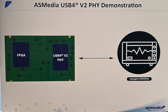
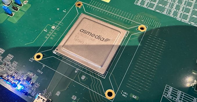
The USB Implementers Forum (USB-IF) introduced USB4 version 2.0 in fall 2022, and it expects systems and devices with the tech to emerge later this year and into next year. These upcoming products will largely rely on Intel's Barlow Ridge controller, a full-featured Thunderbolt 5 controller that goes above and beond the baseline USB4 v2 spec. And though extremely capable, Intel's Thunderbolt controllers are also quite expensive, and Barlow Ridge isn't expected to be any different. Fortunately, for system and device vendors that just need a basic USB4 v2 solution, ASMedia is also working on its own USB4 v2 controller.
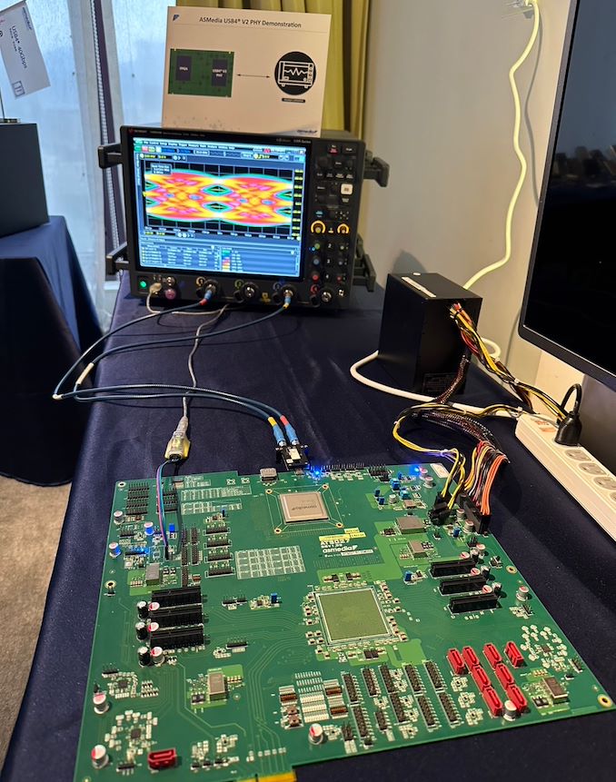
At Computex 2024, ASMedia demonstrated a prototype of its upcoming USB4 v2 physical interface (PHY), which will support USB4 v2's new Gen 4 (160Gbps) data rates and the associated PAM-3 signal encoding. The prototype was implemented using an FPGA, as the company yet has to tape out the completed controller.
Ultimately, the purpose of showing off a FPGA-based PHY at Computex was to allow ASMedia to demonstrate their current PHY design. With the shift to PAM-3 encoding for USB4 v2, ASMedia (and the rest of the USB ecosystem) must develop significantly more complex controllers – and there's no part of that more critical than a solid and reliable PHY design.
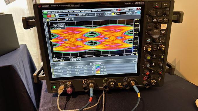
As part of their demonstration, ASMedia had a classic eye diagram display. The eye diagram demoed has a clear opening in the center, which is indicative of good signal integrity, as the larger the eye opening, the less distortion and noise in the signal. The horizontal width of the eye opening represents the time window in which the signal can be sampled correctly, so the relatively narrow horizontal spread of the eye opening suggests that there is minimal jitter, meaning the signal transitions are consistent and predictable. Finally, the vertical height of the eye opening indicates the signal amplitude and the rather tall eye opening suggests a higher signal-to-noise ratio (SNR), meaning that the signal is strong compared to any noise present.
ASMedia itself is one of the major suppliers for discrete USB controllers, so the availability of ASMedia's USB4 v2 chip is crucial for adoption of the standard in general. While Intel will spearhead the industry with their Barlow Ridge Thunderbolt 5/USB4 v2 controller, ASMedia's controller is poised to end up in a far larger range of devices. So the importance of the company's USB4 v2 PHY demo is hard to overstate.
Demos aside, ASMedia is hoping to tape the chip out soon. If all goes well, the company expects their first USB4 v2 controllers to hit the market some time in the second half of 2025.

At FMS 2024, the technological requirements from the storage and memory subsystem took center stage. Both SSD and controller vendors had various demonstrations touting their suitability for different stages of the AI data pipeline - ingestion, preparation, training, checkpointing, and inference. Vendors like Solidigm have different types of SSDs optimized for different stages of the pipeline. At the same time, controller vendors have taken advantage of one of the features introduced recently in the NVM Express standard - Flexible Data Placement (FDP).
FDP involves the host providing information / hints about the areas where the controller could place the incoming write data in order to reduce the write amplification. These hints are generated based on specific block sizes advertised by the device. The feature is completely backwards-compatible, with non-FDP hosts working just as before with FDP-enabled SSDs, and vice-versa.
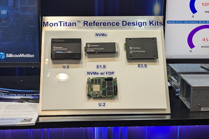
Silicon Motion's MonTitan Gen 5 Enterprise SSD Platform was announced back in 2022. Since then, Silicon Motion has been touting the flexibility of the platform, allowing its customers to incorporate their own features as part of the customization process. This approach is common in the enterprise space, as we have seen with Marvell's Bravera SC5 SSD controller in the DapuStor SSDs and Microchip's Flashtec controllers in the Longsys FORESEE enterprise SSDs.
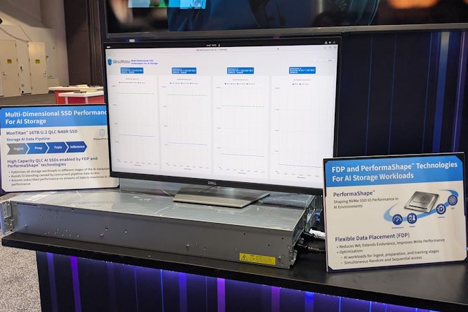
At FMS 2024, the company was demonstrating the advantages of flexible data placement by allowing a single QLC SSD based on their MonTitan platform to take part in different stages of the AI data pipeline while maintaining the required quality of service (minimum bandwidth) for each process. The company even has a trademarked name (PerformaShape) for the firmware feature in the controller that allows the isolation of different concurrent SSD accesses (from different stages in the AI data pipeline) to guarantee this QoS. Silicon Motion claims that this scheme will enable its customers to get the maximum write performance possible from QLC SSDs without negatively impacting the performance of other types of accesses.
Silicon Motion and Phison have market leadership in the client SSD controller market with similar approaches. However, their enterprise SSD controller marketing couldn't be more different. While Phison has gone in for a turnkey solution with their Gen 5 SSD platform (to the extent of not adopting the white label route for this generation, and instead opting to get the SSDs qualified with different cloud service providers themselves), Silicon Motion is opting for a different approach. The flexibility and customization possibilities can make platforms like the MonTitan appeal to flash array vendors.
Storage

Samsung had quietly launched its BM1743 enterprise QLC SSD last month with a hefty 61.44 TB SKU. At FMS 2024, the company had the even larger 122.88 TB version of that SSD on display, alongside a few recorded benchmarking sessions. Compared to the previous generation, the BM1743 comes with a 4.1x improvement in I/O performance, improvement in data retention, and a 45% improvement in power efficiency for sequential writes.

The 128 TB-class QLC SSD boasts of sequential read speeds of 7.5 GBps and write speeds of 3 GBps. Random reads come in at 1.6 M IOPS, while 16 KB random writes clock in at 45K IOPS. Based on the quoted random write access granularity, it appears that Samsung is using a 16 KB indirection unit (IU) to optimize flash management. This is similar to the strategy adopted by Solidigm with IUs larger than 4K in their high-capacity SSDs.
A recorded benchmark session on the company's PM9D3a 8-channel Gen 5 SSD was also on display.

The SSD family is being promoted as a mainstream option for datacenters, and boasts of sequential reads up to 12 GBps and writes up to 6.8 GBps. Random reads clock in at 2 M IOPS, and random writes at 400 K IOPS.

Available in multiple form-factors up to 32 TB (M.2 tops out at 2 TB), the drive's firmware includes optional support for flexible data placement (FDP) to help address the write amplification aspect.
The PM1753 is the current enterprise SSD flagship in Samsung's lineup. With support for 16 NAND channels and capacities up to 32 TB, this U.2 / E3.S SSD has advertised sequential read and write speeds of 14.8 GBps and 11 GBps respectively. Random reads and writes for 4 KB accesses are listed at 3.4 M and 600 K IOPS.

Samsung claims a 1.7x performance improvement and a 1.7x power efficiency improvement over the previous generation (PM1743), making this TLC SSD suitable for AI servers.
The 9th Gen. V-NAND wafer was also available for viewing, though photography was prohibited. Mass production of this flash memory began in April 2024.
Storage
Lorem Ipsum is simply dummy text of the printing and typesetting industry. Lorem Ipsum has been the industry's.
Kioxia's booth at FMS 2024 was a busy one with multiple technology demonstrations keeping visitors occupied. A walk-through of the BiCS 8 manufacturing process was the first to grab my attention. Kioxia and Western Digital announced the sampling of BiCS 8 in March 2023. We had touched briefly upon its CMOS Bonded Array (CBA) scheme in our coverage of Kioxial's 2Tb QLC NAND device and coverage of Western Digital's 128 TB QLC enterprise SSD proof-of-concept demonstration. At Kioxia's booth, we got more insights.
Traditionally, fabrication of flash chips involved placement of the associate logic circuitry (CMOS process) around the periphery of the flash array. The process then moved on to putting the CMOS under the cell array, but the wafer development process was serialized with the CMOS logic getting fabricated first followed by the cell array on top. However, this has some challenges because the cell array requires a high-temperature processing step to ensure higher reliability that can be detrimental to the health of the CMOS logic. Thanks to recent advancements in wafer bonding techniques, the new CBA process allows the CMOS wafer and cell array wafer to be processed independently in parallel and then pieced together, as shown in the models above.
The BiCS 8 3D NAND incorporates 218 layers, compared to 112 layers in BiCS 5 and 162 layers in BiCS 6. The company decided to skip over BiCS 7 (or, rather, it was probably a short-lived generation meant as an internal test vehicle). The generation retains the four-plane charge trap structure of BiCS 6. In its TLC avatar, it is available as a 1 Tbit device. The QLC version is available in two capacities - 1 Tbit and 2 Tbit.
Kioxia also noted that while the number of layers (218) doesn't compare favorably with the latest layer counts from the competition, its lateral scaling / cell shrinkage has enabled it to be competitive in terms of bit density as well as operating speeds (3200 MT/s). For reference, the latest shipping NAND from Micron - the G9 - has 276 layers with a bit density in TLC mode of 21 Gbit/mm2, and operates at up to 3600 MT/s. However, its 232L NAND operates only up to 2400 MT/s and has a bit density of 14.6 Gbit/mm2.
It must be noted that the CBA hybrid bonding process has advantages over the current processes used by other vendors - including Micron's CMOS under array (CuA) and SK hynix's 4D PUC (periphery-under-chip) developed in the late 2010s. It is expected that other NAND vendors will also move eventually to some variant of the hybrid bonding scheme used by Kioxia.
Storage


 and augmented reality (AR) applications by taking advantage of how human vision works. Typically, humans can only perceive detailed imagery in the relatively small central area of our vision called the fovea, while our peripheral vision is much less detailed. Dynamic foveated rendering, in turn, exploits this by using real-time eye tracking to determine where the user is looking, and then rendering just that area in high/full resolution, while rendering the peripheral areas in lower resolution. The net result is that only a fraction of the screen is rendered at full detail, which cuts down on the total amount of rendering work required and boosting framerates on performance-limited devices.</p>
<p style="text-align: center;"><a href="https://www.anandtech.com/show/21432/xpg-demos-nia-handheld-gaming-pc-foveated-rendering-swappable-dram"><img alt="" src="https://images.anandtech.com/doci/21432/IMG_9819_575px.jpg" /></a></p>
<p>As stated before, this technology is sometimes used in high-end AR/VR headsets, where high resolution displays are placed mere inches from one's face. This ends up being an ideal use case for the technique, since at those distances, only a small fraction of the screen is within the fovea.</p>
<p>Using dynamic foveated rendering for a handheld, on the other hand, is a more novel application. All of the same visual principles apply, but the resolutions at play are lower, and the screen is farther from the users' eyes. This makes a handheld device a less ideal use case, at least on paper, as a larger portion of the screen is going to be in the fovea, and thus will need to be rendered at full resolution. None the less, it will be interesting to see how XPG's efforts pan out, and if dynamic foveated rendering is beneficial enough for handheld PCs. As we sometimes see with trade show demos, not everything makes it out of the prototype stage.</p>
<p align="center"><a href="https://www.anandtech.com/show/21432/xpg-demos-nia-handheld-gaming-pc-foveated-rendering-swappable-dram"><img alt="" src="https://images.anandtech.com/doci/21432/IMG_9823_575px.jpg" /></a></p>
<p>According to a press release put out by ADATA ahead of the trade show, the eye tracking technology is being provided by AMD collaborator <a href="https://beam.eyeware.tech/">Eyeware</a>. Notably, their software-based approach runs on top of standard webcams, rather than requiring IR cameras. So the camera hardware itself should be pretty straight-forward.</p>
<p>Foveated rendering aside, XPG is making sure that the Nia won't be a one-trick pony. The handheld's other major claim to fame is its hardware swappability. The prototype handheld not only features a removable M.2-2230 SSD, but the company is also taking advantage of the recently-introduced LPCAMM2 memory module standard to introduce removable DRAM. Via a hatch in the back of the handheld, device owners would be able to swap out LPCAMM2 LPDDR5X modules for higher capacity versions. This would give the handheld an additional degree of future-proofness over current handhelds, which use non-replaceable soldered-down memory.</p>
<p>Rounding out the package, the current prototype is based on an AMD's Zen 4 Phoenix APU, which is used across both of the company's current mobile lines (Ryzen Mobile 7000/8000 and Ryzen Z1). Meanwhile, the unit's display is adjustable, allowing it to be angled away from the body of the handheld.</p>
<p align="center"><a href="https://www.anandtech.com/show/21432/xpg-demos-nia-handheld-gaming-pc-foveated-rendering-swappable-dram"><img alt="" src="https://images.anandtech.com/doci/21432/IMG_9818-678-specs_575px.jpg" /></a></p>
<p>Assuming all goes well with the prototype, XPG aims to release a finished product in 2025.</p>
<p style="text-align: center;"><a href="https://www.anandtech.com/show/21432/xpg-demos-nia-handheld-gaming-pc-foveated-rendering-swappable-dram"><img alt="" src="https://images.anandtech.com/doci/21432/IMG_9824_575px.jpg" /></a></p>
</p> ADATA)
 and augmented reality (AR) applications by taking advantage of how human vision works. Typically, humans can only perceive detailed imagery in the relatively small central area of our vision called the fovea, while our peripheral vision is much less detailed. Dynamic foveated rendering, in turn, exploits this by using real-time eye tracking to determine where the user is looking, and then rendering just that area in high/full resolution, while rendering the peripheral areas in lower resolution. The net result is that only a fraction of the screen is rendered at full detail, which cuts down on the total amount of rendering work required and boosting framerates on performance-limited devices.</p>
<p style="text-align: center;"><a href="https://www.anandtech.com/show/21432/xpg-demos-nia-handheld-gaming-pc-foveated-rendering-swappable-dram"><img alt="" src="https://images.anandtech.com/doci/21432/IMG_9819_575px.jpg" /></a></p>
<p>As stated before, this technology is sometimes used in high-end AR/VR headsets, where high resolution displays are placed mere inches from one's face. This ends up being an ideal use case for the technique, since at those distances, only a small fraction of the screen is within the fovea.</p>
<p>Using dynamic foveated rendering for a handheld, on the other hand, is a more novel application. All of the same visual principles apply, but the resolutions at play are lower, and the screen is farther from the users' eyes. This makes a handheld device a less ideal use case, at least on paper, as a larger portion of the screen is going to be in the fovea, and thus will need to be rendered at full resolution. None the less, it will be interesting to see how XPG's efforts pan out, and if dynamic foveated rendering is beneficial enough for handheld PCs. As we sometimes see with trade show demos, not everything makes it out of the prototype stage.</p>
<p align="center"><a href="https://www.anandtech.com/show/21432/xpg-demos-nia-handheld-gaming-pc-foveated-rendering-swappable-dram"><img alt="" src="https://images.anandtech.com/doci/21432/IMG_9823_575px.jpg" /></a></p>
<p>According to a press release put out by ADATA ahead of the trade show, the eye tracking technology is being provided by AMD collaborator <a href="https://beam.eyeware.tech/">Eyeware</a>. Notably, their software-based approach runs on top of standard webcams, rather than requiring IR cameras. So the camera hardware itself should be pretty straight-forward.</p>
<p>Foveated rendering aside, XPG is making sure that the Nia won't be a one-trick pony. The handheld's other major claim to fame is its hardware swappability. The prototype handheld not only features a removable M.2-2230 SSD, but the company is also taking advantage of the recently-introduced LPCAMM2 memory module standard to introduce removable DRAM. Via a hatch in the back of the handheld, device owners would be able to swap out LPCAMM2 LPDDR5X modules for higher capacity versions. This would give the handheld an additional degree of future-proofness over current handhelds, which use non-replaceable soldered-down memory.</p>
<p>Rounding out the package, the current prototype is based on an AMD's Zen 4 Phoenix APU, which is used across both of the company's current mobile lines (Ryzen Mobile 7000/8000 and Ryzen Z1). Meanwhile, the unit's display is adjustable, allowing it to be angled away from the body of the handheld.</p>
<p align="center"><a href="https://www.anandtech.com/show/21432/xpg-demos-nia-handheld-gaming-pc-foveated-rendering-swappable-dram"><img alt="" src="https://images.anandtech.com/doci/21432/IMG_9818-678-specs_575px.jpg" /></a></p>
<p>Assuming all goes well with the prototype, XPG aims to release a finished product in 2025.</p>
<p style="text-align: center;"><a href="https://www.anandtech.com/show/21432/xpg-demos-nia-handheld-gaming-pc-foveated-rendering-swappable-dram"><img alt="" src="https://images.anandtech.com/doci/21432/IMG_9824_575px.jpg" /></a></p>
</p> ADATA | https://compbuddey.blogspot.com/2024/06/xpg-demos-nia-handheld-gaming-pc-with_22.html)
 and augmented reality (AR) applications by taking advantage of how human vision works. Typically, humans can only perceive detailed imagery in the relatively small central area of our vision called the fovea, while our peripheral vision is much less detailed. Dynamic foveated rendering, in turn, exploits this by using real-time eye tracking to determine where the user is looking, and then rendering just that area in high/full resolution, while rendering the peripheral areas in lower resolution. The net result is that only a fraction of the screen is rendered at full detail, which cuts down on the total amount of rendering work required and boosting framerates on performance-limited devices.</p>
<p style="text-align: center;"><a href="https://www.anandtech.com/show/21432/xpg-demos-nia-handheld-gaming-pc-foveated-rendering-swappable-dram"><img alt="" src="https://images.anandtech.com/doci/21432/IMG_9819_575px.jpg" /></a></p>
<p>As stated before, this technology is sometimes used in high-end AR/VR headsets, where high resolution displays are placed mere inches from one's face. This ends up being an ideal use case for the technique, since at those distances, only a small fraction of the screen is within the fovea.</p>
<p>Using dynamic foveated rendering for a handheld, on the other hand, is a more novel application. All of the same visual principles apply, but the resolutions at play are lower, and the screen is farther from the users' eyes. This makes a handheld device a less ideal use case, at least on paper, as a larger portion of the screen is going to be in the fovea, and thus will need to be rendered at full resolution. None the less, it will be interesting to see how XPG's efforts pan out, and if dynamic foveated rendering is beneficial enough for handheld PCs. As we sometimes see with trade show demos, not everything makes it out of the prototype stage.</p>
<p align="center"><a href="https://www.anandtech.com/show/21432/xpg-demos-nia-handheld-gaming-pc-foveated-rendering-swappable-dram"><img alt="" src="https://images.anandtech.com/doci/21432/IMG_9823_575px.jpg" /></a></p>
<p>According to a press release put out by ADATA ahead of the trade show, the eye tracking technology is being provided by AMD collaborator <a href="https://beam.eyeware.tech/">Eyeware</a>. Notably, their software-based approach runs on top of standard webcams, rather than requiring IR cameras. So the camera hardware itself should be pretty straight-forward.</p>
<p>Foveated rendering aside, XPG is making sure that the Nia won't be a one-trick pony. The handheld's other major claim to fame is its hardware swappability. The prototype handheld not only features a removable M.2-2230 SSD, but the company is also taking advantage of the recently-introduced LPCAMM2 memory module standard to introduce removable DRAM. Via a hatch in the back of the handheld, device owners would be able to swap out LPCAMM2 LPDDR5X modules for higher capacity versions. This would give the handheld an additional degree of future-proofness over current handhelds, which use non-replaceable soldered-down memory.</p>
<p>Rounding out the package, the current prototype is based on an AMD's Zen 4 Phoenix APU, which is used across both of the company's current mobile lines (Ryzen Mobile 7000/8000 and Ryzen Z1). Meanwhile, the unit's display is adjustable, allowing it to be angled away from the body of the handheld.</p>
<p align="center"><a href="https://www.anandtech.com/show/21432/xpg-demos-nia-handheld-gaming-pc-foveated-rendering-swappable-dram"><img alt="" src="https://images.anandtech.com/doci/21432/IMG_9818-678-specs_575px.jpg" /></a></p>
<p>Assuming all goes well with the prototype, XPG aims to release a finished product in 2025.</p>
<p style="text-align: center;"><a href="https://www.anandtech.com/show/21432/xpg-demos-nia-handheld-gaming-pc-foveated-rendering-swappable-dram"><img alt="" src="https://images.anandtech.com/doci/21432/IMG_9824_575px.jpg" /></a></p>
</p> ADATA&body=https://compbuddey.blogspot.com/2024/06/xpg-demos-nia-handheld-gaming-pc-with_22.html)
0 Comments