Hot Posts
Two Is Better Than One: LG Starts Production of 13-inch Tandem OLED Display for Laptops
OLED panels have a number of advantages, including deep blacks, fast response times, and energy efficiency; most of these stemming from the fact that they do not need backlighting. However they also have drawbacks, as well, as trying to drive them to be as bright as a high-tier LCD will quickly wear out the organic material used. Researchers have been spending the past couple of decades developing ways to prolong the lifespans of OLED materials, and recently LG has put together a novel (if brute force) solution: halve the work by doubling the number of pixels. This is the basis of the company's new tandem OLED technology, which has recently gone into mass production.
The Tandem OLED technology introduced by LG Display uses two stacks of red, green, and blue (RGB) organic light-emitting layers, which are layered on top fo each other, essentially reducing how bright each layer needs to individually be in order to hit a specific cumulative brightness. By combining multiple OLED pixels running at a lower brightness, tandem OLED displays are intended to offer higher brightness and durability than traditional single panel OLED displays, reducing the wear on the organic materials in normal situations – and by extension, making it possible to crank up the brightness of the panels well beyond what a single panel could sustain without cooking itself. Overall, LG claims that tandem panels can hit over three-times the brightness of standard OLED panels.
The switch to tandem panels also comes with energy efficiency benefits, as the power consumption of OLED pixels is not linear with the output brightness. According to LG, their tandem panels consume up to 40% less power. More interesting from the manufacturing side of matters, LG's tandem panel stack is 40% thinner (and 28%) lighter than existing OLED laptop screens, despite having to get a whole second layer of pixels in there.
In terms of specifications, the 13-inch tandem OLED panel feature a WQXGA+ (2880×1800) resolution and can cover 100% of the DCI-P3 color gamut. The panel is also certified to meet VESA's Display HDR True Black 500 requirements, which among other things, requires that it can hit 500 nits of brightness. And given that this tech is meant to go into tablets and laptops, it shouldn't come as any surprise that the display panel is also touch sensitive, as well.
"We will continue to strengthen the competitiveness of OLED products for IT applications and offer differentiated customer value based on distinctive strengths of Tandem OLED, such as long life, high brightness, and low power consumption," said Jae-Won Jang, Vice President and Head of the Medium Display Product Planning Division at LG Display.
Without any doubts, LG's Tandem OLED display panel looks impressive. The company is banking on it doing well in the high-end laptop and tablet markets, where manufacturers have been somewhat hesitant to embrace OLED displays due to power concerns. The technology has already been adopted by Apple for their most recent iPad Pro tablets, and now LG is making it available to a wider group of OEMs.
What remains to be seen is the technology's cost. Computer-grade OLED panels are already a more expensive option, and this one ups the ante with two layers of OLED pixels. So it isn't a question of whether it will be reserved for premium, high-margin devices, but a matter of just how much it will add to the final price tag.
For now, LG Display does not disclose which PC OEMs are set to use its 13-inch Tandem OLED panel, though as the company is a supplier to virtually all of the PC OEMs, there's little doubt it should crop up in multiple laptops soon enough.
DisplaysPopular Post
Kioxia Details BiCS 8 NAND at FMS 2024: 218 Layers With Superior Scaling Kioxia's booth at FMS 2024 was a busy one with multiple technology demonstrations keeping visitors occupied. A walk-through of the BiCS 8 manufacturing process was the first to grab my attention. Kioxia and Western Digital announced the sampling of BiCS 8 in March 2023. We had touched briefly upon its CMOS Bonded Array (CBA) scheme in our coverage of Kioxial's 2Tb QLC NAND device and coverage of Western Digital's 128 TB QLC enterprise SSD proof-of-concept demonstration. At Kioxia's booth, we got more insights.
Traditionally, fabrication of flash chips involved placement of the associate logic circuitry (CMOS process) around the periphery of the flash array. The process then moved on to putting the CMOS under the cell array, but the wafer development process was serialized with the CMOS logic getting fabricated first followed by the cell array on top. However, this has some challenges because the cell array requires a high-temperature processing step to ensure higher reliability that can be detrimental to the health of the CMOS logic. Thanks to recent advancements in wafer bonding techniques, the new CBA process allows the CMOS wafer and cell array wafer to be processed independently in parallel and then pieced together, as shown in the models above.
The BiCS 8 3D NAND incorporates 218 layers, compared to 112 layers in BiCS 5 and 162 layers in BiCS 6. The company decided to skip over BiCS 7 (or, rather, it was probably a short-lived generation meant as an internal test vehicle). The generation retains the four-plane charge trap structure of BiCS 6. In its TLC avatar, it is available as a 1 Tbit device. The QLC version is available in two capacities - 1 Tbit and 2 Tbit.
Kioxia also noted that while the number of layers (218) doesn't compare favorably with the latest layer counts from the competition, its lateral scaling / cell shrinkage has enabled it to be competitive in terms of bit density as well as operating speeds (3200 MT/s). For reference, the latest shipping NAND from Micron - the G9 - has 276 layers with a bit density in TLC mode of 21 Gbit/mm2, and operates at up to 3600 MT/s. However, its 232L NAND operates only up to 2400 MT/s and has a bit density of 14.6 Gbit/mm2.
It must be noted that the CBA hybrid bonding process has advantages over the current processes used by other vendors - including Micron's CMOS under array (CuA) and SK hynix's 4D PUC (periphery-under-chip) developed in the late 2010s. It is expected that other NAND vendors will also move eventually to some variant of the hybrid bonding scheme used by Kioxia.
Storage
DeepCool Adds Vapor Chamber to an Air Cooler: AIO-Like Performance at Air Cooler Reliability While the market for high-end CPU coolers has decidedly shifted towards closed-loop all-in-one liquid coolers over the last several years, air cooling remains alive and well. Even at the high-end, there are still further improvements and innovations being made, such as DeepCool's vapor chamber-based tower cooler, which was demonstrated at Computex.
Named the Assassin IV VC Vision, DeepCool's design is an advanced concept vehicle that equips a tower cooled with both a vapor chamber in the base as well as has an LCD pad on top for extra flourish. The vapor chamber is said to increase the cooling capacity by 20W, adding a bit more of an edge to an already very powerful tower cooler design.
While we expect this one to come to market eventually, don't be surprised if both vapor chamber and the screen to land on other products together or separately. For example, the massive DeepCool Assassin IV VC Vision has a more compact brother that has a screen and a vapor chamber.
The unit builds on top of the already monstrous DeepCool Assassin IV that comes with seven 0.6-mm heat pipes and can mount up to three 120/140mm fans, depending on installation (one is magnetically attached). With a weight of 1.575 kilograms – almost entirely copper and aluminum – this one is already good enough to cool down even the highest-performing CPUs.
DeepCool is currently trying to figure out recommended pricing for its Assassin IV VC Vision cooler, but the original Assassin IV costs $99.99, so expect the unit with a vapor chamber and a screen to build on top of that.
Cases/Cooling/PSUs
Search This Blog
OfferNest
Subscribe Us
Most Popular
Kioxia Details BiCS 8 NAND at FMS 2024: 218 Layers With Superior Scaling Kioxia's booth at FMS 2024 was a busy one with multiple technology demonstrations keeping visitors occupied. A walk-through of the BiCS 8 manufacturing process was the first to grab my attention. Kioxia and Western Digital announced the sampling of BiCS 8 in March 2023. We had touched briefly upon its CMOS Bonded Array (CBA) scheme in our coverage of Kioxial's 2Tb QLC NAND device and coverage of Western Digital's 128 TB QLC enterprise SSD proof-of-concept demonstration. At Kioxia's booth, we got more insights.
Traditionally, fabrication of flash chips involved placement of the associate logic circuitry (CMOS process) around the periphery of the flash array. The process then moved on to putting the CMOS under the cell array, but the wafer development process was serialized with the CMOS logic getting fabricated first followed by the cell array on top. However, this has some challenges because the cell array requires a high-temperature processing step to ensure higher reliability that can be detrimental to the health of the CMOS logic. Thanks to recent advancements in wafer bonding techniques, the new CBA process allows the CMOS wafer and cell array wafer to be processed independently in parallel and then pieced together, as shown in the models above.
The BiCS 8 3D NAND incorporates 218 layers, compared to 112 layers in BiCS 5 and 162 layers in BiCS 6. The company decided to skip over BiCS 7 (or, rather, it was probably a short-lived generation meant as an internal test vehicle). The generation retains the four-plane charge trap structure of BiCS 6. In its TLC avatar, it is available as a 1 Tbit device. The QLC version is available in two capacities - 1 Tbit and 2 Tbit.
Kioxia also noted that while the number of layers (218) doesn't compare favorably with the latest layer counts from the competition, its lateral scaling / cell shrinkage has enabled it to be competitive in terms of bit density as well as operating speeds (3200 MT/s). For reference, the latest shipping NAND from Micron - the G9 - has 276 layers with a bit density in TLC mode of 21 Gbit/mm2, and operates at up to 3600 MT/s. However, its 232L NAND operates only up to 2400 MT/s and has a bit density of 14.6 Gbit/mm2.
It must be noted that the CBA hybrid bonding process has advantages over the current processes used by other vendors - including Micron's CMOS under array (CuA) and SK hynix's 4D PUC (periphery-under-chip) developed in the late 2010s. It is expected that other NAND vendors will also move eventually to some variant of the hybrid bonding scheme used by Kioxia.
Storage
DeepCool Adds Vapor Chamber to an Air Cooler: AIO-Like Performance at Air Cooler Reliability While the market for high-end CPU coolers has decidedly shifted towards closed-loop all-in-one liquid coolers over the last several years, air cooling remains alive and well. Even at the high-end, there are still further improvements and innovations being made, such as DeepCool's vapor chamber-based tower cooler, which was demonstrated at Computex.
Named the Assassin IV VC Vision, DeepCool's design is an advanced concept vehicle that equips a tower cooled with both a vapor chamber in the base as well as has an LCD pad on top for extra flourish. The vapor chamber is said to increase the cooling capacity by 20W, adding a bit more of an edge to an already very powerful tower cooler design.
While we expect this one to come to market eventually, don't be surprised if both vapor chamber and the screen to land on other products together or separately. For example, the massive DeepCool Assassin IV VC Vision has a more compact brother that has a screen and a vapor chamber.
The unit builds on top of the already monstrous DeepCool Assassin IV that comes with seven 0.6-mm heat pipes and can mount up to three 120/140mm fans, depending on installation (one is magnetically attached). With a weight of 1.575 kilograms – almost entirely copper and aluminum – this one is already good enough to cool down even the highest-performing CPUs.
DeepCool is currently trying to figure out recommended pricing for its Assassin IV VC Vision cooler, but the original Assassin IV costs $99.99, so expect the unit with a vapor chamber and a screen to build on top of that.
Cases/Cooling/PSUs
Intel Issues Official Statement Regarding 14th and 13th Gen Instability, Recommends Intel Default Settings Further to our last piece which we detailed Intel's issue to motherboard vendors to follow with stock power settings for Intel's 14th and 13th Gen Core series processors, Intel has now issued a follow-up statement to this. Over the last week or so, motherboard vendors quickly released firmware updates with a new profile called 'Intel Baseline', which motherboard vendors assumed would address the instability issues.
As it turns out, Intel doesn't seem to accept this as technically, these Intel Baseline profiles are not to be confused with Intel's default specifications. This means that Intel's Baseline profiles seemingly give the impression that they are operating at default settings, hence the terminology 'baseline' used, but this still opens motherboard vendors to use their interpretations of MCE or Multi-Core Enhancement.
To clarify things for consumers, Intel has sent us the following statement:
Several motherboard manufacturers have released BIOS profiles labeled ‘Intel Baseline Profile’. However, these BIOS profiles are not the same as the 'Intel Default Settings' recommendations that Intel has recently shared with its partners regarding the instability issues reported on 13th and 14th gen K SKU processors.
These ‘Intel Baseline Profile’ BIOS settings appear to be based on power delivery guidance previously provided by Intel to manufacturers describing the various power delivery options for 13th and 14th Generation K SKU processors based on motherboard capabilities.
Intel is not recommending motherboard manufacturers to use ‘baseline’ power delivery settings on boards capable of higher values.
Intel’s recommended ‘Intel Default Settings’ are a combination of thermal and power delivery features along with a selection of possible power delivery profiles based on motherboard capabilities.
Intel recommends customers to implement the highest power delivery profile compatible with each individual motherboard design as noted in the table below:
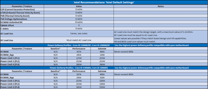
Click to Enlarge Intel's Default Settings
What Intel's statement is effectively saying to consumers, is that users shouldn't be using the Baseline Power Delivery profiles which are offered by motherboard vendors through a plethora of firmware updates. Instead, Intel is recommending users opt for Intel Default Settings, which follows what the specific processor is rated for by Intel out of the box to achieve the clock speeds advertised, without users having to worry about firmware 'over' optimization which can cause instability as there have been many reports of happening.
Not only this, but the Intel Default settings offer a combination of thermal specifications and power capabilities, including voltage and frequency curve settings that apply to the capability of the motherboard used, and the power delivery equipped on the motherboard. At least for the most part, Intel is recommending users with 14th and 13th-Gen Core series K, KF, and KS SKUs that they do not recommend users opt in using the Baseline profiles offered by motherboard vendors.
Digesting the contrast between the two statements, the key differential is that Intel's priority is reducing the current going through the processor, which for both the 14th and 13th Gen Core series processors is a maximum of 400 A, even when using the Extreme profile. We know those motherboard vendors on their Z790 and Z690 motherboards opt for an unrestricted power profile, which is essentially 'unlimited' power and current to maximize performance at the cost of power consumption and heat, which does exacerbate problems and can lead to frequent bouts of instability, especially on high-intensity workloads.
Another variable Intel is recommending is that the AC Load Line must match the design target of the processor, with a maximum value of 1.1 mOhm, and that the DC Load Line must be ... CPUs
Several motherboard manufacturers have released BIOS profiles labeled ‘Intel Baseline Profile’. However, these BIOS profiles are not the same as the 'Intel Default Settings' recommendations that Intel has recently shared with its partners regarding the instability issues reported on 13th and 14th gen K SKU processors.
These ‘Intel Baseline Profile’ BIOS settings appear to be based on power delivery guidance previously provided by Intel to manufacturers describing the various power delivery options for 13th and 14th Generation K SKU processors based on motherboard capabilities.
Intel is not recommending motherboard manufacturers to use ‘baseline’ power delivery settings on boards capable of higher values.
Intel’s recommended ‘Intel Default Settings’ are a combination of thermal and power delivery features along with a selection of possible power delivery profiles based on motherboard capabilities.
Intel recommends customers to implement the highest power delivery profile compatible with each individual motherboard design as noted in the table below:

Click to Enlarge Intel's Default Settings
Kioxia Details BiCS 8 NAND at FMS 2024: 218 Layers With Superior Scaling Kioxia's booth at FMS 2024 was a busy one with multiple technology demonstrations keeping visitors occupied. A walk-through of the BiCS 8 manufacturing process was the first to grab my attention. Kioxia and Western Digital announced the sampling of BiCS 8 in March 2023. We had touched briefly upon its CMOS Bonded Array (CBA) scheme in our coverage of Kioxial's 2Tb QLC NAND device and coverage of Western Digital's 128 TB QLC enterprise SSD proof-of-concept demonstration. At Kioxia's booth, we got more insights.
Traditionally, fabrication of flash chips involved placement of the associate logic circuitry (CMOS process) around the periphery of the flash array. The process then moved on to putting the CMOS under the cell array, but the wafer development process was serialized with the CMOS logic getting fabricated first followed by the cell array on top. However, this has some challenges because the cell array requires a high-temperature processing step to ensure higher reliability that can be detrimental to the health of the CMOS logic. Thanks to recent advancements in wafer bonding techniques, the new CBA process allows the CMOS wafer and cell array wafer to be processed independently in parallel and then pieced together, as shown in the models above.
The BiCS 8 3D NAND incorporates 218 layers, compared to 112 layers in BiCS 5 and 162 layers in BiCS 6. The company decided to skip over BiCS 7 (or, rather, it was probably a short-lived generation meant as an internal test vehicle). The generation retains the four-plane charge trap structure of BiCS 6. In its TLC avatar, it is available as a 1 Tbit device. The QLC version is available in two capacities - 1 Tbit and 2 Tbit.
Kioxia also noted that while the number of layers (218) doesn't compare favorably with the latest layer counts from the competition, its lateral scaling / cell shrinkage has enabled it to be competitive in terms of bit density as well as operating speeds (3200 MT/s). For reference, the latest shipping NAND from Micron - the G9 - has 276 layers with a bit density in TLC mode of 21 Gbit/mm2, and operates at up to 3600 MT/s. However, its 232L NAND operates only up to 2400 MT/s and has a bit density of 14.6 Gbit/mm2.
It must be noted that the CBA hybrid bonding process has advantages over the current processes used by other vendors - including Micron's CMOS under array (CuA) and SK hynix's 4D PUC (periphery-under-chip) developed in the late 2010s. It is expected that other NAND vendors will also move eventually to some variant of the hybrid bonding scheme used by Kioxia.
Storage
Intel Sells Its Arm Shares, Reduces Stakes in Other Companies Intel has divested its entire stake in Arm Holdings during the second quarter, raising approximately $147 million. Alongside this, Intel sold its stake in cybersecurity firm ZeroFox and reduced its holdings in Astera Labs, all as part of a broader effort to manage costs and recover cash amid significant financial challenges.
The sale of Intel's 1.18 million shares in Arm Holdings, as reported in a recent SEC filing, comes at a time when the company is struggling with substantial financial losses. Despite the $147 million generated from the sale, Intel reported a $120 million net loss on its equity investments for the quarter, which is a part of a larger $1.6 billion loss that Intel faced during this period.
In addition to selling its stake in Arm, Intel also exited its investment in ZeroFox and reduced its involvement with Astera Labs, a company known for developing connectivity platforms for enterprise hardware. These moves are in line with Intel's strategy to reduce costs and stabilize its financial position as it faces ongoing market challenges.
Despite the divestment, Intel's past investment in Arm was likely driven by strategic considerations. Arm Holdings is a significant force in the semiconductor industry, with its designs powering most mobile devices, and, for obvious reasons, Intel would like to address these. Intel and Arm are also collaborating on datacenter platforms tailored for Intel's 18A process technology. Additionally, Arm might view Intel as a potential licensee for its technologies and a valuable partner for other companies that license Arm's designs.
Intel's investment in Astera Labs was also a strategic one as the company probably wanted to secure steady supply of smart retimers, smart cable modems, and CXL memory controller, which are used in volumes in datacenters and Intel is certainly interested in selling as many datacenter CPUs as possible.
Intel's financial struggles were highlighted earlier this month when the company released a disappointing earnings report, which led to a 33% drop in its stock value, erasing billions of dollars of capitalization. To counter these difficulties, Intel announced plans to cut 15,000 jobs and implement other expense reductions. The company has also suspended its dividend, signaling the depth of its efforts to conserve cash and focus on recovery. When it comes to divestment of Arm stock, the need for immediate financial stabilization has presumably taken precedence, leading to the decision.
CPUs
Tags
- https://www.amazon.com/2020-2021-Planner-Academic-Do-Twin-Wire/dp/B083V11TM5?tag=all0ad0-21https://m.media-amazon.com/images/I/41btLRSWksL.jpg
- https://www.amazon.com/Acid-Dreams-Complete-History-Sixties-ebook/dp/B005012G6U?tag=all0ad0-21https://m.media-amazon.com/images/I/51SwQkWyzAL.jpg
- https://www.amazon.com/Adaptive-Charging-Charger-Compatible-EP-TA20JBE/dp/B07NPD5T5H?tag=all0ad0-21https://m.media-amazon.com/images/I/419ZKbzdOwL.jpg
- https://www.amazon.com/Adjustable-Foldable-Portable-Compatible-Smartphones/dp/B0963PBY4C?tag=all0ad0-21https://m.media-amazon.com/images/I/51p4wF13kCL.jpg
- https://www.amazon.com/African-Twisted-Headwraps-Headband-Headscarf/dp/B09FDMKTZP?tag=all0ad0-21https://m.media-amazon.com/images/I/41WGbzL+RkL.jpg
- https://www.amazon.com/AINOPE-Charging-Braided-compatible-MacBook/dp/B094YDZQ1C?tag=all0ad0-21https://m.media-amazon.com/images/I/51ppc0xIVtL.jpg
- https://www.amazon.com/Ambergris-Saints-Madmen-Shriek-Finch/dp/B08GGCSN3S?tag=all0ad0-21https://m.media-amazon.com/images/I/51zgVCTiUiL.jpg
- https://www.amazon.com/Amplim-Hospital-Thermometer-Professional-Thermometer/dp/B0865R5H82?tag=all0ad0-21https://m.media-amazon.com/images/I/31K01H4s6UL.jpg
- https://www.amazon.com/Animal-Gaming-Electronic-Lights-Birthday/dp/B0B2QTLWMS?tag=all0ad0-21https://m.media-amazon.com/images/I/41GY22qHwkL.jpg
- https://www.amazon.com/Animals-Flashcards-Children-Alphabet-cards/dp/9811168881?tag=all0ad0-21https://m.media-amazon.com/images/I/51U2gcSb62L.jpg
- https://www.amazon.com/ANNKIE-Dance-Electronic-Lights-Birthday/dp/B0B74DVQQV?tag=all0ad0-21https://m.media-amazon.com/images/I/51K45aP99DL.jpg
- https://www.amazon.com/Anti-Wrinkle-Silicone-Reusable-D%C3%A9collet%C3%A9-Eliminate/dp/B07FQ3QV1C?tag=all0ad0-21https://m.media-amazon.com/images/I/41RhHEsEi3L.jpg
- https://www.amazon.com/anyloop-Military-Smartwatch-Bluetooth-Waterproof/dp/B0C4P7R6CK?tag=all0ad0-21https://m.media-amazon.com/images/I/41lUAHTmi5L.jpg
- https://www.amazon.com/Aromatherapy-Shower-Steamers-Relaxation-Everything/dp/B08QDKWBWS?tag=all0ad0-21https://m.media-amazon.com/images/I/613KwmLJJ1L.jpg
- https://www.amazon.com/Audible-A-Rose-in-Winter/dp/B09JHTGT14?tag=all0ad0-21https://m.media-amazon.com/images/I/51z1bVj4CxL.jpg
- https://www.amazon.com/Audible-Fall-School-Good-Evil/dp/B0B8SZY3P5?tag=all0ad0-21https://m.media-amazon.com/images/I/51MWO0bOLIL.jpg
- https://www.amazon.com/Audible-Termination-Shock-A-Novel/dp/B09556Y79B?tag=all0ad0-21https://m.media-amazon.com/images/I/51jEsfJXG3S.jpg
- https://www.amazon.com/Automatic-Toddlers-Operated-Batteries-Birthday/dp/B0BZH34G2G?tag=all0ad0-21https://m.media-amazon.com/images/I/51PQaTAouaL.jpg
- https://www.amazon.com/AWGOU-Baby-Wipes-Dispenser-Large-Capacity/dp/B0BS3K9BFV?tag=all0ad0-21https://m.media-amazon.com/images/I/41emlsr6WnL.jpg
- https://www.amazon.com/AYAO-Blades-8-Inch-12TPI-2-Pack/dp/B0C9C1VB3D?tag=all0ad0-21https://m.media-amazon.com/images/I/41jMumgfJ4L.jpg
- https://www.amazon.com/Backless-Sleeve-Ribbed-Fitted-Shirts/dp/B0B68KPGP8?tag=all0ad0-21https://m.media-amazon.com/images/I/41vB0uLnuzL.jpg
- https://www.amazon.com/BCHWAY-Stuffed-Storage-Beanbag-Organizer/dp/B09WR2KPPG?tag=all0ad0-21https://m.media-amazon.com/images/I/41GBr+1tEBL.jpg
- https://www.amazon.com/beeprt-Bluetooth-Shipping-Label-Printer/dp/B0BK93ZSNC?tag=all0ad0-21https://m.media-amazon.com/images/I/41Ufm05KrJL.jpg
- https://www.amazon.com/Benewid-Creami-Pints-Lids-Containers/dp/B0C85Q44N6?tag=all0ad0-21https://m.media-amazon.com/images/I/41bFv6o0xjL.jpg
- https://www.amazon.com/BIG-TEETH-Magnetic-Microfiber-5-Piece/dp/B0BRXBM2T9?tag=all0ad0-21https://m.media-amazon.com/images/I/51BCt4B8jDL.jpg
- https://www.amazon.com/Blackbeard-Americas-Most-Notorious-Pirate/dp/B086N4X4SG?tag=all0ad0-21https://m.media-amazon.com/images/I/51fqeuICW+L.jpg
- https://www.amazon.com/Blaster-Automatic-Toddlers-Christmas-Birthday/dp/B0CCV9RDM5?tag=all0ad0-21https://m.media-amazon.com/images/I/51j8FkZtBiL.jpg
- https://www.amazon.com/Bloodline-Jess-Lourey/dp/1542016312?tag=all0ad0-21https://m.media-amazon.com/images/I/51KLqBsOIbL.jpg
- https://www.amazon.com/Bracelet-Stainless-Zirconium-Ceramic-Statement/dp/B0B2CQR5YW?tag=all0ad0-21https://m.media-amazon.com/images/I/41iUmnfsAmL.jpg
- https://www.amazon.com/Bride-Shadow-King-Book/dp/B0B75RL7DX?tag=all0ad0-21https://m.media-amazon.com/images/I/51LyIt-n5+L.jpg
- https://www.amazon.com/Bright-Empires-House-Spirit-Shadow/dp/B08T4VG1S2?tag=all0ad0-21https://m.media-amazon.com/images/I/61-JxjVNClL.jpg
- https://www.amazon.com/BRIGHTWORLD-Stuffers-Upgrade-5-9inch-Birthday/dp/B0B6RBCYZ7?tag=all0ad0-21https://m.media-amazon.com/images/I/61pQaIf3NVL.jpg
- https://www.amazon.com/Bunfly-Clipper-Grooming-Suction-Capacity/dp/B0C6PMSY3Z?tag=all0ad0-21https://m.media-amazon.com/images/I/51ig7m1g9OL.jpg
- https://www.amazon.com/C412H-Spring-Wound-Commercial-12-Hour-Automatic/dp/B00CTW2LYA?tag=all0ad0-21https://m.media-amazon.com/images/I/41QNVA+3MRL.jpg
- https://www.amazon.com/Cardone-Select-84-832-Ignition-Distributor/dp/B000CFFAYY?tag=all0ad0-21https://m.media-amazon.com/images/I/414iGfzryML.jpg
- https://www.amazon.com/ceiba-tree-Graduation-Envelopes-Classroom/dp/B0BQQKSLFK?tag=all0ad0-21https://m.media-amazon.com/images/I/51ZOS4YOvzL.jpg
- https://www.amazon.com/CellElection-Elastic-Ponytail-Holders-Straight/dp/B09TFDLR85?tag=all0ad0-21https://m.media-amazon.com/images/I/514QbooGKKL.jpg
- https://www.amazon.com/Certified-Charger-Charging-Braveridge-Lightning/dp/B0C1VKRXN1?tag=all0ad0-21https://m.media-amazon.com/images/I/41XG+lopk8L.jpg
- https://www.amazon.com/Certified%E3%80%91-Charger-Fasting-Charging-Compatible/dp/B0C489SXGB?tag=all0ad0-21https://m.media-amazon.com/images/I/41dNzZS3BML.jpg
- https://www.amazon.com/Charger-Certified-Lightning-Charging-Compatible/dp/B0C4L9S7QH?tag=all0ad0-21https://m.media-amazon.com/images/I/514iP4Fy28L.jpg
- https://www.amazon.com/Chicken-Shredder-Ergonomic-Anti-Slip-Dishwasher/dp/B0C5R1KZP6?tag=all0ad0-21https://m.media-amazon.com/images/I/61cx6f737WL.jpg
- https://www.amazon.com/Christmas-Decorations-PHITRIC-Sparkling-Fireplace/dp/B0B7WNC93J?tag=all0ad0-21https://m.media-amazon.com/images/I/51Gv07W+JCL.jpg
- https://www.amazon.com/Christmas-Snowflake-Stamping-Manicure-Designer/dp/B09L4SV5YY?tag=all0ad0-21https://m.media-amazon.com/images/I/51TQJxPWLrL.jpg
- https://www.amazon.com/Cleaning-Bathroom-Crevice-Bristle-Multifunctional/dp/B0CDBK4C9T?tag=all0ad0-21https://m.media-amazon.com/images/I/415dsUeaDmL.jpg
- https://www.amazon.com/Clinic-Crohns-Disease-Ulcerative-Colitis-ebook/dp/B09ZBLJLFL?tag=all0ad0-21https://m.media-amazon.com/images/I/41f5FHJle+L.jpg
- https://www.amazon.com/Coasters-Absorbent-Ceramic-Coaster-Housewarming/dp/B09ZKJRSLH?tag=all0ad0-21https://m.media-amazon.com/images/I/51POqbEgyOL.jpg
- https://www.amazon.com/CoBak-Rotating-Case-iPad-Generation/dp/B0BBR8MFHM?tag=all0ad0-21https://m.media-amazon.com/images/I/516NR1N0QKL.jpg
- https://www.amazon.com/COLORFULLEAF-Bamboo-Underwear-Breathable-Trunks/dp/B0B9BX5S9L?tag=all0ad0-21https://m.media-amazon.com/images/I/31MYPhHHapL.jpg
- https://www.amazon.com/Comforter-Paisley-Microfiber-Bohemian-Pillowcases/dp/B0BZP1SC6F?tag=all0ad0-21https://m.media-amazon.com/images/I/51KkoN3AgNL.jpg
- https://www.amazon.com/Compressed-Cordless-Electric-Brushless-Portable/dp/B0BBR1XHLS?tag=all0ad0-21https://m.media-amazon.com/images/I/41dJ2sJpGjL.jpg
- https://www.amazon.com/Cordking-14-Protectors-Shockproof-Microfiber/dp/B0B6GKRCGM?tag=all0ad0-21https://m.media-amazon.com/images/I/41tXMeWi5FL.jpg
- https://www.amazon.com/Cordless-High-Speed-Brushless-Lightweight-Cleaners/dp/B0CGL8NBM8?tag=all0ad0-21https://m.media-amazon.com/images/I/41NfsXSEnLL.jpg
- https://www.amazon.com/Cordless-Straightening-Travel-Wireless-Straightener/dp/B0CJ2HQL3H?tag=all0ad0-21https://m.media-amazon.com/images/I/31wTmdUZyuL.jpg
- https://www.amazon.com/Corrector-Clavicle-Adjustable-Straightener-Providing/dp/B07L41CV8B?tag=all0ad0-21https://m.media-amazon.com/images/I/41B0xbK2kRL.jpg
- https://www.amazon.com/Court-Wizard-Terry-Mancour-audiobook/dp/B07PC2RQSC?tag=all0ad0-21https://m.media-amazon.com/images/I/512jFQbt6JL.jpg
- https://www.amazon.com/Cozivwaiy-Platform-Sandals-Studded-Evening/dp/B0BM43W7VF?tag=all0ad0-21https://m.media-amazon.com/images/I/41+RFM1gP7L.jpg
- https://www.amazon.com/Crenova-Magnetic-Construction-Preschool-Educational/dp/B0CC1RZ2BJ?tag=all0ad0-21https://m.media-amazon.com/images/I/51lJxAlaL3L.jpg
- https://www.amazon.com/Dan-Darci-Marbling-Paint-Kids/dp/B08CLVVJ8C?tag=all0ad0-21https://m.media-amazon.com/images/I/61nDIOC0B0L.jpg
- https://www.amazon.com/Dash-Cam-Front-BOOGIIO-Dashboard/dp/B08LZJ8GMH?tag=all0ad0-21https://m.media-amazon.com/images/I/41B3QK42N1L.jpg
- https://www.amazon.com/Democracy-America-What-Wrong-About-ebook/dp/B0867TRV52?tag=all0ad0-21https://m.media-amazon.com/images/I/4129LSadlmL.jpg
- https://www.amazon.com/Detailing-Attachment-Scrubber-Cleaning-Upholstery/dp/B07WGKQVN7?tag=all0ad0-21https://m.media-amazon.com/images/I/41K75BhGaML.jpg
- https://www.amazon.com/Diameter-Hydrophilic-Filtration-Non-sterile-COBETTER/dp/B0B7BB3L1R?tag=all0ad0-21https://m.media-amazon.com/images/I/31KD4E7TW5L.jpg
- https://www.amazon.com/Diamond-Organizer-Jewelry-Storage-Diamonds/dp/B08JLVSZ15?tag=all0ad0-21https://m.media-amazon.com/images/I/514Z+bbZfQL.jpg
- https://www.amazon.com/Diamond-Painting-Diamonds-12x16inch-30%C3%9740cm/dp/B09X1CQJHX?tag=all0ad0-21https://m.media-amazon.com/images/I/51xEpqCkI-L.jpg
- https://www.amazon.com/didforu-Monocular-Telescope-Monoscope-Binocular/dp/B0C3757D5G?tag=all0ad0-21https://m.media-amazon.com/images/I/512qer0p1oL.jpg
- https://www.amazon.com/Dinkhiiro-Outdoor-Pickleball-Balls-Pickle-Ball-Accessories-Pickleball/dp/B0BNQ8HM76?tag=all0ad0-21https://m.media-amazon.com/images/I/41ni+GPR71L.jpg
- https://www.amazon.com/Distant-Horizon-Backyard-Starship-Book/dp/B0BDP9RPQL?tag=all0ad0-21https://m.media-amazon.com/images/I/512FYS+c9wL.jpg
- https://www.amazon.com/Dorman-1650134-Chevrolet-Driver-Assembly/dp/B00JW1XGDG?tag=all0ad0-21https://m.media-amazon.com/images/I/51p-ja2Vc9L.jpg
- https://www.amazon.com/DosTutu-Mermaid-Costume-Pageant-Birthday/dp/B09NJK6K9M?tag=all0ad0-21https://m.media-amazon.com/images/I/51pVYQBZKJL.jpg
- https://www.amazon.com/dp/B09GFWPXWH?tag=all0ad0-21https://m.media-amazon.com/images/I/51xO7ZL-sVL.jpg
- https://www.amazon.com/DREAMS-VISIONS-Jesus-Awakening-Muslim-ebook/dp/B0078FAA3M?tag=all0ad0-21https://m.media-amazon.com/images/I/51BKVftuXDL.jpg
- https://www.amazon.com/DSJUGGLING-Transparent-Two-Tone-Juggling-Beginners/dp/B09WHRZCFF?tag=all0ad0-21https://m.media-amazon.com/images/I/419NOeSGijL.jpg
- https://www.amazon.com/Empire-of-Storms-Sarah-J-Maas-audiobook/dp/B01KIQV5EU?tag=all0ad0-21https://m.media-amazon.com/images/I/51EMceUgxFL.jpg
- https://www.amazon.com/Eniucow-Montessori-Permanent-Traction-Toddlers/dp/B0B7CZ9KGN?tag=all0ad0-21https://m.media-amazon.com/images/I/31bJyZYqhJL.jpg
- https://www.amazon.com/Eslazoer-insulated-neoprene-reusable-activity/dp/B0BKSMXVN8?tag=all0ad0-21https://m.media-amazon.com/images/I/41kTXH2JxBL.jpg
- https://www.amazon.com/Everyday-Solutions-Mug-Tree-Polished/dp/B0B4T6NCML?tag=all0ad0-21https://m.media-amazon.com/images/I/31-7RTd1fUL.jpg
- https://www.amazon.com/Extender-Universal-Rotatable-Extension-Attachment/dp/B0C4YLVH3D?tag=all0ad0-21https://m.media-amazon.com/images/I/41+YysChcFL.jpg
- https://www.amazon.com/Eyelash-Extension-Cleanser-BREYLEE-Shampoo/dp/B08RJFTFN4?tag=all0ad0-21https://m.media-amazon.com/images/I/51UncwwSzwL.jpg
- https://www.amazon.com/Fatal-Discord-Michael-Massing-audiobook/dp/B078YDCMBD?tag=all0ad0-21https://m.media-amazon.com/images/I/51AJdROll+L.jpg
- https://www.amazon.com/Faucet-Sprayer-Attachment-Replacement-included/dp/B0BCFMT7WY?tag=all0ad0-21https://m.media-amazon.com/images/I/31wZDbk-bYL.jpg
- https://www.amazon.com/Feeling-Good-David-D-Burns-audiobook/dp/B01N9TCVLD?tag=all0ad0-21https://m.media-amazon.com/images/I/51ixV6lf9AL.jpg
- https://www.amazon.com/FeelinGirl-Waitsted-Shapewear-Control-Lifting/dp/B0CBK29G76?tag=all0ad0-21https://m.media-amazon.com/images/I/31Cl6qaK0HL.jpg
- https://www.amazon.com/Fenceguru-Decorative-Rustproof-Barrier-Landscape/dp/B0BZ91ZPHF?tag=all0ad0-21https://m.media-amazon.com/images/I/519kGS3sjxL.jpg
- https://www.amazon.com/Fernco-PQC-105-Flexible-Reusable-Plastic/dp/B00CFVNCCK?tag=all0ad0-21https://m.media-amazon.com/images/I/21xcHMaS37L.jpg
- https://www.amazon.com/Floating-Shelves-Bathroom-Bedroom-Kitchen/dp/B0CF8J497J?tag=all0ad0-21https://m.media-amazon.com/images/I/51cT9HpSh4L.jpg
- https://www.amazon.com/Forehead-Thermometer-Infrared-Eligible-Indicator/dp/B0B4ZD6K43?tag=all0ad0-21https://m.media-amazon.com/images/I/31J97vQVUHL.jpg
- https://www.amazon.com/FRGROW-Lights-Spectrum-Function-Gooseneck/dp/B0CC4P13L7?tag=all0ad0-21https://m.media-amazon.com/images/I/51UXtap-56L.jpg
- https://www.amazon.com/Funrous-Mattress-Lifter-Helper-Stainless/dp/B09WMZPM1N?tag=all0ad0-21https://m.media-amazon.com/images/I/31Vg6rJibzL.jpg
- https://www.amazon.com/GAOY-Glassy-Foundation-Combination-Polish/dp/B0BD4MMFVM?tag=all0ad0-21https://m.media-amazon.com/images/I/414wIShbm+L.jpg
- https://www.amazon.com/Gay-Pride-Rainbow-Heart-Silicone/dp/B01J8E5NUA?tag=all0ad0-21https://m.media-amazon.com/images/I/31TtNjUl3uL.jpg
- https://www.amazon.com/Gerod-Compatible-Replacement-Cushions-Headphones/dp/B09BPV34ZB?tag=all0ad0-21https://m.media-amazon.com/images/I/41cXXPmWNoL.jpg
- https://www.amazon.com/GetKen-Dispenser-Rechargeable-Portable-Automatic/dp/B0C4T26LK4?tag=all0ad0-21https://m.media-amazon.com/images/I/41v5jE7AsIL.jpg
- https://www.amazon.com/Gifts-Girls-birthday-Toys-Duplication/dp/B0B6FY328P?tag=all0ad0-21https://m.media-amazon.com/images/I/51mMmkuwdfL.jpg
- https://www.amazon.com/Girls-Charm-Bracelet-Making-Kit/dp/B0CFCC8HBZ?tag=all0ad0-21https://m.media-amazon.com/images/I/81-SB1q4h1L.jpg
- https://www.amazon.com/Girls-Charm-Bracelet-Making-Kit/dp/B0CFF3SLJT?tag=all0ad0-21https://m.media-amazon.com/images/I/81kJ83iM+IL.jpg
- https://www.amazon.com/GloFX-Blue-Rave-Bedroom-Decor/dp/B0B7ZXG6PS?tag=all0ad0-21https://m.media-amazon.com/images/I/41iPdpfs1DL.jpg
- https://www.amazon.com/GMSOL-Diamond-Necklaces-Necklace-Layered/dp/B0BXKY3XW9?tag=all0ad0-21https://m.media-amazon.com/images/I/21iQgpW3i4L.jpg
- https://www.amazon.com/Greenland-Home-GL-THROWSH-Shangri-La-Throw/dp/B017U6U8JO?tag=all0ad0-21https://m.media-amazon.com/images/I/61VISLraXWL.jpg
- https://www.amazon.com/Gyierwe-High-Pressure-Stainless-Adjustable-Filtration/dp/B0C5RHCSN8?tag=all0ad0-21https://m.media-amazon.com/images/I/51RZ3tTLzyL.jpg
- https://www.amazon.com/Halloween-Decorations-Indoor-DECSPAS-Haunted/dp/B0C6JPZ6K5?tag=all0ad0-21https://m.media-amazon.com/images/I/51zSmWVx7HL.jpg
- https://www.amazon.com/HawSkgFub-Curtains-Farmhouse-Seasonal-Bathroom/dp/B0BVLTJR4P?tag=all0ad0-21https://m.media-amazon.com/images/I/412k-TN9yzL.jpg
- https://www.amazon.com/Helping-Soldering-Hand-Base-Microscope/dp/B0BBR46ZQ9?tag=all0ad0-21https://m.media-amazon.com/images/I/41IZoepkAkL.jpg
- https://www.amazon.com/Her-Soul-Take-Souls-Trilogy/dp/B0BDT2M2QZ?tag=all0ad0-21https://m.media-amazon.com/images/I/51Z1AUkTytL.jpg
- https://www.amazon.com/HISANDUK-Pendant-Fixtures-Kitchen-Adjustable/dp/B0B76G6VCT?tag=all0ad0-21https://m.media-amazon.com/images/I/41SzQX+tAeL.jpg
- https://www.amazon.com/Homeleo-Operated-Christmas-Strawberry-Decorations/dp/B07WTVGTWX?tag=all0ad0-21https://m.media-amazon.com/images/I/51+CNn9QowL.jpg
- https://www.amazon.com/House-of-Impossible-Beauties-audiobook/dp/B077VQ68HH?tag=all0ad0-21https://m.media-amazon.com/images/I/51VFkDIrDsL.jpg
- https://www.amazon.com/HOUSE-Organizer-Upgraded-Undersink-Organizers/dp/B0BY8XZK71?tag=all0ad0-21https://m.media-amazon.com/images/I/510FKKVDhpL.jpg
- https://www.amazon.com/House-Witch-Humorous-Romantic-Fantasy/dp/B0BLJ7CQKK?tag=all0ad0-21https://m.media-amazon.com/images/I/61+JJSw9jZL.jpg
- https://www.amazon.com/HR-Quadcopter-Beginners-Altitude-Batteries/dp/B08L8YFT4S?tag=all0ad0-21https://m.media-amazon.com/images/I/41pf-DNDj5L.jpg
- https://www.amazon.com/Humble-Chic-Wall-Art-Prints/dp/B07QL3GTX4?tag=all0ad0-21https://m.media-amazon.com/images/I/31QO1OLNDGL.jpg
- https://www.amazon.com/Huyerdo-Corduroy-Cosmetic-Aesthetic-Organizer/dp/B0C1YXPX5M?tag=all0ad0-21https://m.media-amazon.com/images/I/51Es7IjWzjL.jpg
- https://www.amazon.com/I-Invited-Her-In-Adele-Parks-audiobook/dp/B07JZGFFHY?tag=all0ad0-21https://m.media-amazon.com/images/I/51ak3gyHziL.jpg
- https://www.amazon.com/In1docom-Peanut-Massage-Massager-Lacrosse/dp/B0CB4S2JRX?tag=all0ad0-21https://m.media-amazon.com/images/I/41sBnhqhZzL.jpg
- https://www.amazon.com/INeedIt-D101-Portable-Wireless-Organization/dp/B0BCKV8B81?tag=all0ad0-21https://m.media-amazon.com/images/I/21OGF1G7x9L.jpg
- https://www.amazon.com/Inflatable-Ground-Dustproof-Rainproof-Waterproof/dp/B0CB8B4PKX?tag=all0ad0-21https://m.media-amazon.com/images/I/51o0yuVrjPL.jpg
- https://www.amazon.com/Insane-Labz-Bitartrate-AMPiberry-Endurance/dp/B07V6JCWJG?tag=all0ad0-21https://m.media-amazon.com/images/I/51GZtu2lUZL.jpg
- https://www.amazon.com/Island-Queen-A-Novel/dp/B08MLPY619?tag=all0ad0-21https://m.media-amazon.com/images/I/51snO62ltvL.jpg
- https://www.amazon.com/J-hong-Toddlers-Learning-Montessori-Christmas/dp/B0C4LK67Q5?tag=all0ad0-21https://m.media-amazon.com/images/I/51q4mMYfoLL.jpg
- https://www.amazon.com/jalz-Wooden-Spoons-Cooking-3-Piece/dp/B07DZKTC9B?tag=all0ad0-21https://m.media-amazon.com/images/I/416iXJ1B8PL.jpg
- https://www.amazon.com/JENN-ARDOR-Fashion-Sneakers-Comfortable/dp/B08N16X7HR?tag=all0ad0-21https://m.media-amazon.com/images/I/41y+m0CTBeS.jpg
- https://www.amazon.com/John-Sterling-Sports-7-Ball-Capacity/dp/B01DWSH1I0?tag=all0ad0-21https://m.media-amazon.com/images/I/31-O3z3v+XL.jpg
- https://www.amazon.com/Jorpet-Elevated-Adjustable-Non-Slip-Stainless/dp/B0C3YRH31J?tag=all0ad0-21https://m.media-amazon.com/images/I/41+P1DIyA0L.jpg
- https://www.amazon.com/JOYMODE-women-workout-clothes-Legging/dp/B08766FN91?tag=all0ad0-21https://m.media-amazon.com/images/I/31DoD7LD8EL.jpg
- https://www.amazon.com/Kettlebell-Whiskey-Shaped-Silicone-Melting/dp/B0C5NBXHDF?tag=all0ad0-21https://m.media-amazon.com/images/I/41XwetcdbXL.jpg
- https://www.amazon.com/Kingdom-Come-Backyard-Starship-Book/dp/B0BKBRDCV2?tag=all0ad0-21https://m.media-amazon.com/images/I/51DX-OPQv6L.jpg
- https://www.amazon.com/Kitchen-BAYZZ-Cushioned-Non-Slip-Waterproof/dp/B095GZYG7Z?tag=all0ad0-21https://m.media-amazon.com/images/I/41-vM6JlCeL.jpg
- https://www.amazon.com/KOIOS-Immersion-Multifunctional-Stainless-Titanium/dp/B076GW89V9?tag=all0ad0-21https://m.media-amazon.com/images/I/41YrmEtdu0L.jpg
- https://www.amazon.com/Lady-Orc-Sworn-Book/dp/B0B4BB9B21?tag=all0ad0-21https://m.media-amazon.com/images/I/51VsjpQ+WoL.jpg
- https://www.amazon.com/Large-Multipurpose-Waterproof-Picnic-Shopping/dp/B0CCS1HSMK?tag=all0ad0-21https://m.media-amazon.com/images/I/410kS6OJJHL.jpg
- https://www.amazon.com/Large-Multipurpose-Waterproof-Picnic-Shopping/dp/B0CF58TZ9J?tag=all0ad0-21https://m.media-amazon.com/images/I/410kS6OJJHL.jpg
- https://www.amazon.com/Lay-My-Heart-Angela-Pneuman-ebook/dp/B00FJ5EQ0Q?tag=all0ad0-21https://m.media-amazon.com/images/I/419DBRj4HuL.jpg
- https://www.amazon.com/LeadDock-Ice-Cube-Tray-Lid/dp/B0CB6TN9DY?tag=all0ad0-21https://m.media-amazon.com/images/I/51WpROdbWEL.jpg
- https://www.amazon.com/Learning-Educational-Preschool-Developmental-Montessori/dp/B0BY2HBQLS?tag=all0ad0-21https://m.media-amazon.com/images/I/510R2-67PbL.jpg
- https://www.amazon.com/LEDKINGDOMUS-inches-Driving-Compatible-Pickup/dp/B09176936Z?tag=all0ad0-21https://m.media-amazon.com/images/I/416I+aay3RL.jpg
- https://www.amazon.com/Legend-Randidly-Ghosthound-LitRPG-Adventure/dp/B09CR88G8L?tag=all0ad0-21https://m.media-amazon.com/images/I/51cte+pTRVL.jpg
- https://www.amazon.com/Legend-Randidly-Ghosthound-LitRPG-Adventure/dp/B09NB32VS5?tag=all0ad0-21https://m.media-amazon.com/images/I/51HquIJf4EL.jpg
- https://www.amazon.com/Legend-Randidly-Ghosthound-LitRPG-Adventure/dp/B09WTLH4Z9?tag=all0ad0-21https://m.media-amazon.com/images/I/61j-pJq9blL.jpg
- https://www.amazon.com/LENRUE-Computer-Speakers-Desktop-AUX_Black/dp/B0BRFN13S9?tag=all0ad0-21https://m.media-amazon.com/images/I/41XeSj+qShL.jpg
- https://www.amazon.com/LIANTRAL-Firewood-Outdoor-Upgrade-Fireplace/dp/B0BKSVRW4N?tag=all0ad0-21https://m.media-amazon.com/images/I/51Y9mIZmocL.jpg
- https://www.amazon.com/Lilys-White-Lace-Carolyn-Brown-ebook/dp/B00DTTW5UW?tag=all0ad0-21https://m.media-amazon.com/images/I/51iPZWUaUQL.jpg
- https://www.amazon.com/LISEN-Magnetic-Install-Friendly-Smartphones/dp/B07YRKDF4P?tag=all0ad0-21https://m.media-amazon.com/images/I/51tMoOMiRzL.jpg
- https://www.amazon.com/LJIOEZZI-Balaclava-Weather-Snowboarding-Motorcycling/dp/B0BHVNYM8Z?tag=all0ad0-21https://m.media-amazon.com/images/I/31YRjxzYi8L.jpg
- https://www.amazon.com/LOXP-2C-CAR-Sun-Shade-Umbrella-Medium/dp/B0BR7WLLY4?tag=all0ad0-21https://m.media-amazon.com/images/I/41vWPHUEsJL.jpg
- https://www.amazon.com/LUENX-Trendy-Oversized-Aviator-Sunglasses/dp/B09CMB5D7N?tag=all0ad0-21https://m.media-amazon.com/images/I/41uZsi7kskL.jpg
- https://www.amazon.com/MAGEFY-Eyelashes-Natural-Handmade-Reusable/dp/B0956V789H?tag=all0ad0-21https://m.media-amazon.com/images/I/51UgJTxfm2S.jpg
- https://www.amazon.com/Magnetic-Birthday-Building-Preschool-Montessori/dp/B0BWWPC5MR?tag=all0ad0-21https://m.media-amazon.com/images/I/61UuS8o90ZL.jpg
- https://www.amazon.com/Makartt-Extension-Glitter-Trendy-Builder/dp/B096VQW7NF?tag=all0ad0-21https://m.media-amazon.com/images/I/31hUzSIu6gL.jpg
- https://www.amazon.com/Makeup-Brush-Holder-Travel-Essentials/dp/B0C7G5YXRZ?tag=all0ad0-21https://m.media-amazon.com/images/I/31od+KNxUkL.jpg
- https://www.amazon.com/MaraFansie-Housewarming-Birthday-Anniversary-Graduation/dp/B0BS416GJ3?tag=all0ad0-21https://m.media-amazon.com/images/I/51QjF6NaQ+L.jpg
- https://www.amazon.com/MAREE-Face-Moisturizer-Anti-Wrinkle-Hyaluronic/dp/B0C3LXWJJ7?tag=all0ad0-21https://m.media-amazon.com/images/I/512NgLTHbTL.jpg
- https://www.amazon.com/Matter-Black-Lives-Writing-Yorker/dp/B08TP4YC6S?tag=all0ad0-21https://m.media-amazon.com/images/I/513aBwlCG-L.jpg
- https://www.amazon.com/Mavericks-Craig-Alanson-audiobook/dp/B07GH5ZJ3N?tag=all0ad0-21https://m.media-amazon.com/images/I/51OW+MpwHYL.jpg
- https://www.amazon.com/McAfee-Protection-Exclusive-Monitoring-Subscription/dp/B0BB2N69J8?tag=all0ad0-21https://m.media-amazon.com/images/I/510kxZvrlKL.jpg
- https://www.amazon.com/McAfee-Protection-Unlimited-Device-Download/dp/B07BFRVMMN?tag=all0ad0-21https://m.media-amazon.com/images/I/51qNb5s7JzL.jpg
- https://www.amazon.com/McAfee-Total-Protection-Devices-Subscription/dp/B07K98XDX8?tag=all0ad0-21https://m.media-amazon.com/images/I/51P0zntKKaL.jpg
- https://www.amazon.com/McAfee-Total-Protection-Devices-Subscription/dp/B07K995RWG?tag=all0ad0-21https://m.media-amazon.com/images/I/51hk1owA-eL.jpg
- https://www.amazon.com/McClusky-Battle-Midway-David-Rigby-ebook/dp/B07NJCKM5P?tag=all0ad0-21https://m.media-amazon.com/images/I/41wKgBrbEhL.jpg
- https://www.amazon.com/Meat-Thermometer-Digital-Grilling-Cooking/dp/B0BQ782XNW?tag=all0ad0-21https://m.media-amazon.com/images/I/51cOJyK7rHL.jpg
- https://www.amazon.com/Missing-Molly-Natalie-Barelli-audiobook/dp/B07N7HZ9XJ?tag=all0ad0-21https://m.media-amazon.com/images/I/41G2D08UIgL.jpg
- https://www.amazon.com/Mondays-Not-Coming-audiobook/dp/B07B7897X8?tag=all0ad0-21https://m.media-amazon.com/images/I/51BRoON6IWL.jpg
- https://www.amazon.com/Monster-Wireless-Bluetooth-Headphones-Rotating/dp/B097JZQXXL?tag=all0ad0-21https://m.media-amazon.com/images/I/41RciianoPL.jpg
- https://www.amazon.com/Moolan-Cordless-Portable-Powerful-Rechargeable/dp/B0CB1C743Z?tag=all0ad0-21https://m.media-amazon.com/images/I/41qRyj2A+xL.jpg
- https://www.amazon.com/MORNEEX-Polyester-Bathroom-Waterproof-72X72inches/dp/B0B712Q9QD?tag=all0ad0-21https://m.media-amazon.com/images/I/41ejnaDrS0L.jpg
- https://www.amazon.com/MOYEIKH-Talking-Elderly-Visually-Impaired/dp/B0C4LCMTNN?tag=all0ad0-21https://m.media-amazon.com/images/I/41m7k3YEUXL.jpg
- https://www.amazon.com/Mr-You-Organizer-ModelsStand-Dust-proof-Velvet%EF%BC%8C12L/dp/B082X6BCJG?tag=all0ad0-21https://m.media-amazon.com/images/I/51cRFT9gZCL.jpg
- https://www.amazon.com/MUJERBAY-Massager-Compression-Full-Cover-Fasciitis/dp/B0BWJ4LT32?tag=all0ad0-21https://m.media-amazon.com/images/I/41d7tUceqaL.jpg
- https://www.amazon.com/Musashi-audiobook/dp/B07FXMJCX6?tag=all0ad0-21https://m.media-amazon.com/images/I/515t3Zygd7L.jpg
- https://www.amazon.com/MUSICOZY-Headphones-Bluetooth-Headband-Waterproof/dp/B09NN1MJQS?tag=all0ad0-21https://m.media-amazon.com/images/I/41qxlHs2CTL.jpg
- https://www.amazon.com/My-Dear-Hamilton-audiobook/dp/B077NN1WWF?tag=all0ad0-21https://m.media-amazon.com/images/I/51sBrSA5VfL.jpg
- https://www.amazon.com/NATOLIKE-Pickleball-Lightweight-Fiberglass-Polypropylene/dp/B0BY8JF32S?tag=all0ad0-21https://m.media-amazon.com/images/I/61I+i2U7+sL.jpg
- https://www.amazon.com/Natrol-High-Potency-Antioxidant-Vitamin-Tablets/dp/B08KXGJXR1?tag=all0ad0-21https://m.media-amazon.com/images/I/41y11UVSqkL.jpg
- https://www.amazon.com/Necromancer-Spellmonger-Book-10/dp/B083YVZ8YQ?tag=all0ad0-21https://m.media-amazon.com/images/I/51FELytNyCL.jpg
- https://www.amazon.com/NeoLartes-July-White-Berry-Garlands/dp/B0BWDHKFWV?tag=all0ad0-21https://m.media-amazon.com/images/I/51P3USHQMCL.jpg
- https://www.amazon.com/Neoprene-Dumbbell-Weights-Anti-slip-Anti-roll/dp/B087JDLWLQ?tag=all0ad0-21https://m.media-amazon.com/images/I/31hKC3UgF7L.jpg
- https://www.amazon.com/NEW-Norton-AntiVirus-Plus-Antivirus/dp/B07Q69X7XL?tag=all0ad0-21https://m.media-amazon.com/images/I/51M35ZaPBmL.jpg
- https://www.amazon.com/Nexillumi-LED-Lights-60-75-Inch/dp/B07XBJR7GY?tag=all0ad0-21https://m.media-amazon.com/images/I/519sc2GYDnL.jpg
- https://www.amazon.com/Nicebay-Professional-Dryerwith3-Attachments-Lightweight/dp/B0CBSHRBS6?tag=all0ad0-21https://m.media-amazon.com/images/I/41Og2LDzcML.jpg
- https://www.amazon.com/Night-Sleep-Death-Stars-Novel/dp/B07XY9SKT3?tag=all0ad0-21https://m.media-amazon.com/images/I/51bBRM-4BUL.jpg
- https://www.amazon.com/NuLink-Electric-Inflation-Decoration-110V-120V/dp/B01H2QF6SK?tag=all0ad0-21https://m.media-amazon.com/images/I/41mdv0LnxfL.jpg
- https://www.amazon.com/Nylavee-Computer-Speakers-Soundbar-Connection/dp/B0BZCMM17X?tag=all0ad0-21https://m.media-amazon.com/images/I/41GYynP1rrL.jpg
- https://www.amazon.com/Oakland-Living-Rose-Bird-Bath/dp/B000PAKVJK?tag=all0ad0-21https://m.media-amazon.com/images/I/41MzpuSS3yL.jpg
- https://www.amazon.com/Oasis-033879-001-VersaFiller-Filter-Cartridge/dp/B002WDQGXS?tag=all0ad0-21https://m.media-amazon.com/images/I/41nyJPxi4SL.jpg
- https://www.amazon.com/OBL-Plastic-Durable-Non-deformable-Imitation/dp/B07SKJ946F?tag=all0ad0-21https://m.media-amazon.com/images/I/51Z2NMJGOwL.jpg
- https://www.amazon.com/OCHYIT-Protector-Waterproof-Defender-Analyzer/dp/B0BKL8DWQR?tag=all0ad0-21https://m.media-amazon.com/images/I/41XownI6MdL.jpg
- https://www.amazon.com/Oil-Sprayer-Dispenser-Accessories-Spritzer/dp/B0B93CBCFC?tag=all0ad0-21https://m.media-amazon.com/images/I/51nNMZPYUXL.jpg
- https://www.amazon.com/OKIMO-Wireless-Computer-Ergonomic-Chromebook/dp/B0CC4KLTKM?tag=all0ad0-21https://m.media-amazon.com/images/I/41LJQ8jNxZL.jpg
- https://www.amazon.com/Organizer-Buttonholes-Stretchable-Connectable-Adjustable/dp/B0C22ZMRWC?tag=all0ad0-21https://m.media-amazon.com/images/I/51ql4-4eN8L.jpg
- https://www.amazon.com/Organizer-organizer-Zippers-Blocking-Insert%EF%BC%8C5/dp/B07WMWCBTQ?tag=all0ad0-21https://m.media-amazon.com/images/I/310UEu-zi7L.jpg
- https://www.amazon.com/ORICO-Adapter-External-Converter-Transfer/dp/B0B3MMJ1LB?tag=all0ad0-21https://m.media-amazon.com/images/I/41dfdJx68AL.jpg
- https://www.amazon.com/Original-Certified-Charging-Lightning-Compatible/dp/B0CJDHYYZD?tag=all0ad0-21https://m.media-amazon.com/images/I/41trxkrOxLL.jpg
- https://www.amazon.com/Oupeng-sky-Carabiner-Clip-Ring/dp/B07MSBZ7BZ?tag=all0ad0-21https://m.media-amazon.com/images/I/51Bxk8se22L.jpg
- https://www.amazon.com/Over-Top-Jonathan-Van-Ness-audiobook/dp/B07Q386LM5?tag=all0ad0-21https://m.media-amazon.com/images/I/51rcfpVI5UL.jpg
- https://www.amazon.com/Padfolio-Portfolio-Interview-Document-Organizer/dp/B07VLPS9ZK?tag=all0ad0-21https://m.media-amazon.com/images/I/41CSIOr0ZoL.jpg
- https://www.amazon.com/Pairs-Heavy-Ratchet-Tie-Mount-Crossbar-Easy/dp/B0725Z9LSB?tag=all0ad0-21https://m.media-amazon.com/images/I/41xI-f4Jj9L.jpg
- https://www.amazon.com/Paperwhite-Generation-Signature-Lightweight-Transparent/dp/B0C8B1JJYZ?tag=all0ad0-21https://m.media-amazon.com/images/I/41MpXChQpIL.jpg
- https://www.amazon.com/Paw-Patrol-Collectible-DIE-CAST-Vehicles/dp/B07S6VH6DD?tag=all0ad0-21https://m.media-amazon.com/images/I/41nC9yFe1dL.jpg
- https://www.amazon.com/Peace-nest-Checkered-Checkerboard-Lightweight/dp/B0BX969J3C?tag=all0ad0-21https://m.media-amazon.com/images/I/51D8BO3dasL.jpg
- https://www.amazon.com/Perfect-Run-Book/dp/B09SVMRP12?tag=all0ad0-21https://m.media-amazon.com/images/I/51zkV2RkC2L.jpg
- https://www.amazon.com/Pet-Grooming-Brush-Double-Sided-Blue/dp/B0BRPZY67Z?tag=all0ad0-21https://m.media-amazon.com/images/I/41iA2Z29chL.jpg
- https://www.amazon.com/Pieces-Washed-Reversible-Cooling-Closure/dp/B094FGZ3XD?tag=all0ad0-21https://m.media-amazon.com/images/I/41hX+gmSQvL.jpg
- https://www.amazon.com/PINHEN-Stabilizer-360%C2%B0Rotate-Hands-Free-Compatible/dp/B09N8VL6VT?tag=all0ad0-21https://m.media-amazon.com/images/I/41j3QfO4JLL.jpg
- https://www.amazon.com/Planner-2023-2024-Academic-Calendar-Hardcover/dp/B0BP22KCYV?tag=all0ad0-21https://m.media-amazon.com/images/I/51xfDnKUkSL.jpg
- https://www.amazon.com/Ponytail-hoyuwak-Rhinestone-Accessories-Silver/dp/B0C1GRQNLM?tag=all0ad0-21https://m.media-amazon.com/images/I/51Jl+ePN1vL.jpg
- https://www.amazon.com/Portable-Wireless-Espresso-Machine-Freshly-brewed/dp/B09LCKLYGT?tag=all0ad0-21https://m.media-amazon.com/images/I/21uyv4z55pL.jpg
- https://www.amazon.com/Premom-Quantitative-Ovulation-Predictor-Numerical/dp/B07P7LSW57?tag=all0ad0-21https://m.media-amazon.com/images/I/51dY9dReMhL.jpg
- https://www.amazon.com/Professional-Pedicure-Rosmax-Stainless-Washable/dp/B08TM7TH1N?tag=all0ad0-21https://m.media-amazon.com/images/I/519tcTL-K8L.jpg
- https://www.amazon.com/Projector-Bluetooth-15000Lumens-Portable-Compatible/dp/B0CGXHVB5D?tag=all0ad0-21https://m.media-amazon.com/images/I/414hYl+AJuL.jpg
- https://www.amazon.com/Projector-Control-Bluetooth-Dimmable-Projection/dp/B09F95JS41?tag=all0ad0-21https://m.media-amazon.com/images/I/61GYRolZ-9L.jpg
- https://www.amazon.com/Projector-HOMPOW-Bluetooth-Correction-Compatible/dp/B0BCKV1VHX?tag=all0ad0-21https://m.media-amazon.com/images/I/616j3cS2O9L.jpg
- https://www.amazon.com/Protector-Coverage-Protection-Installation-Specially/dp/B0B87THFLK?tag=all0ad0-21https://m.media-amazon.com/images/I/41tlgaNVLCL.jpg
- https://www.amazon.com/Protectors-Furniture-Scratches-Hardwood-Large/dp/B0CHB4ZR22?tag=all0ad0-21https://m.media-amazon.com/images/I/51UIaW9XlXL.jpg
- https://www.amazon.com/Purifier-Purifiers-VEWIOR-Settings-Ultra-Quiet/dp/B0B41Z7B6H?tag=all0ad0-21https://m.media-amazon.com/images/I/41o0rCSrKcL.jpg
- https://www.amazon.com/Purifiers-Purifier-Aromatherapy-Function-Filtration/dp/B0C5GCPDV2?tag=all0ad0-21https://m.media-amazon.com/images/I/41KvpYD7k5L.jpg
- https://www.amazon.com/QAWDAWM-Conduction-Headphones-Bluetooth-Waterproof/dp/B0CGR1799N?tag=all0ad0-21https://m.media-amazon.com/images/I/41trzwTzdKL.jpg
- https://www.amazon.com/REDESS-Beanie-Women-Winter-Slouchy/dp/B0BZVDHFNJ?tag=all0ad0-21https://m.media-amazon.com/images/I/51hHyl+rkWL.jpg
- https://www.amazon.com/Robot-Vacuum-Mop-Combo-Self-Charging/dp/B0CD3XTMS1?tag=all0ad0-21https://m.media-amazon.com/images/I/518O5sALu1L.jpg
- https://www.amazon.com/RONGPRO-Combination-Carpenter-Zinc-Alloy-Die-Casting/dp/B09GVQRZVK?tag=all0ad0-21https://m.media-amazon.com/images/I/41uHEayHMEL.jpg
- https://www.amazon.com/ROOMLIFE-Chenille-Slipcover-Loveseat-Sectional/dp/B0BJ5T5Z91?tag=all0ad0-21https://m.media-amazon.com/images/I/51VNyhUtziL.jpg
- https://www.amazon.com/Ryan-Rule-York-Ruthless-Book/dp/B0BPJSLNDX?tag=all0ad0-21https://m.media-amazon.com/images/I/51o9mZQpbgL.jpg
- https://www.amazon.com/Sandstorm-Street-Rats-Aramoor-Book/dp/B09QDYGXGT?tag=all0ad0-21https://m.media-amazon.com/images/I/61g7nbsvDiL.jpg
- https://www.amazon.com/Santoku-Knife-Stainless-Ergonomic-Restaurant/dp/B0865TNBKC?tag=all0ad0-21https://m.media-amazon.com/images/I/41bVfVBEhOL.jpg
- https://www.amazon.com/SATC-Woodworking-Carpenters-Gardening-Resistant/dp/B09WYGJJ3F?tag=all0ad0-21https://m.media-amazon.com/images/I/31U+zqjEzNL.jpg
- https://www.amazon.com/Scissors-ULG-Hairdressing-Stainless-Detachable/dp/B09ZTZYDT2?tag=all0ad0-21https://m.media-amazon.com/images/I/315+PnPQhmL.jpg
- https://www.amazon.com/SeaVees-Mens-Standard-Casual-Sneaker/dp/B008TUCU1A?tag=all0ad0-21https://m.media-amazon.com/images/I/31z4PJ-dnQL.jpg
- https://www.amazon.com/Security-Lighting-Waterproof-Outdoor-Basketball/dp/B09GV2B545?tag=all0ad0-21https://m.media-amazon.com/images/I/41Hh9Px9UzL.jpg
- https://www.amazon.com/Shadow-Dark-Queen-Serpentwar-Saga/dp/B07YCT8PKM?tag=all0ad0-21https://m.media-amazon.com/images/I/517+deIbkiL.jpg
- https://www.amazon.com/Shadowplay-Spellmonger-Legacy-Secrets-Book/dp/B09DZ4S8MG?tag=all0ad0-21https://m.media-amazon.com/images/I/51mV-QcOzOL.jpg
- https://www.amazon.com/Shamrocks-Bedroom-Bathroom-Kitchen-Hallway/dp/B07ZV5DSTN?tag=all0ad0-21https://m.media-amazon.com/images/I/51J0KqPk6ML.jpg
- https://www.amazon.com/Silicone-Reusable-AiKanbo-Airtight-Preservation/dp/B09X1LXS9B?tag=all0ad0-21https://m.media-amazon.com/images/I/41fNI3t5hYS.jpg
- https://www.amazon.com/Sixriver-Crimper-Straightener-Crimping-Volumizing/dp/B0C85XZFM8?tag=all0ad0-21https://m.media-amazon.com/images/I/51OrfENeNCL.jpg
- https://www.amazon.com/Skyfoot-Adjustable-Increase-Insoles-Cushioning/dp/B0BN5V3PPF?tag=all0ad0-21https://m.media-amazon.com/images/I/41uwN2FiiiL.jpg
- https://www.amazon.com/skysen-Magnetic-Decorative-Handles-Hardware/dp/B07L72D7FX?tag=all0ad0-21https://m.media-amazon.com/images/I/51AIynaJumL.jpg
- https://www.amazon.com/STAR-WARS-SW-Halloween-Wookiee/dp/B0BHZVTNQV?tag=all0ad0-21https://m.media-amazon.com/images/I/411fjZsBYrL.jpg
- https://www.amazon.com/Stens-375-402-Black-Decker-82-020/dp/B01H5K2QSQ?tag=all0ad0-21https://m.media-amazon.com/images/I/21Tkj5Btb0L.jpg
- https://www.amazon.com/Stickers-Bottles-Waterproof-Animals-Skateboard/dp/B09S3JSNV3?tag=all0ad0-21https://m.media-amazon.com/images/I/61E2JiiBkML.jpg
- https://www.amazon.com/Still-Just-Geek-Annotated-Memoir/dp/B09HZB3WGP?tag=all0ad0-21https://m.media-amazon.com/images/I/51Ee05wyCwL.jpg
- https://www.amazon.com/Straightener-MiroPure-Straightening-Anti-Scald-Temperature/dp/B06XGXP9RP?tag=all0ad0-21https://m.media-amazon.com/images/I/41okvbcUEnL.jpg
- https://www.amazon.com/Summit-Treestands-Replacement-Cables-Climbing/dp/B001BAGLXI?tag=all0ad0-21https://m.media-amazon.com/images/I/41vANZDPuCL.jpg
- https://www.amazon.com/Support-Car-Car-Support-Memory-Car-Driving/dp/B07MV5X84K?tag=all0ad0-21https://m.media-amazon.com/images/I/51iEP2LoKmL.jpg
- https://www.amazon.com/Surface-Charger-Microsoft-Compatible-Laptop/dp/B0BW41H1W2?tag=all0ad0-21https://m.media-amazon.com/images/I/31Xt8mDjKyL.jpg
- https://www.amazon.com/Survival-Essentials-Tactical-Emergency-Activities/dp/B0BFFC8ZTV?tag=all0ad0-21https://m.media-amazon.com/images/I/512QQyOIcjL.jpg
- https://www.amazon.com/SwaggWood-Certified-Lightning-Charging-Compatible/dp/B0CFQF6LS6?tag=all0ad0-21https://m.media-amazon.com/images/I/41vq56QWFNL.jpg
- https://www.amazon.com/Tablecloth-Disposable-Surfboard-Rectangle-Birthday/dp/B09X2GK6Z7?tag=all0ad0-21https://m.media-amazon.com/images/I/51M30CIsW2L.jpg
- https://www.amazon.com/Tanming-Womens-Seamless-Workout-Running/dp/B0BHY73PWB?tag=all0ad0-21https://m.media-amazon.com/images/I/310AJZGSfCL.jpg
- https://www.amazon.com/Tear-off-Productivity-Anna-Marie-Collections/dp/B09GDDCMJP?tag=all0ad0-21https://m.media-amazon.com/images/I/41yZVQwPEZL.jpg
- https://www.amazon.com/Textures-Graphite-Charcoal-Steven-Pearce-ebook/dp/B01N7Y0XP5?tag=all0ad0-21https://m.media-amazon.com/images/I/61XIPXXBL5L.jpg
- https://www.amazon.com/The-Beginning-of-Everything-audiobook/dp/B081NXJVT5?tag=all0ad0-21https://m.media-amazon.com/images/I/51aG06izsLL.jpg
- https://www.amazon.com/The-Enlightenment/dp/B07VHFHN3Y?tag=all0ad0-21https://m.media-amazon.com/images/I/51ArbS5NSDL.jpg
- https://www.amazon.com/The-Good-Lie/dp/B08QVNGF3M?tag=all0ad0-21https://m.media-amazon.com/images/I/51UPMGqzseS.jpg
- https://www.amazon.com/Thermal-Moisture-Wicking-Breathable-Charcoal/dp/B0929CZSL2?tag=all0ad0-21https://m.media-amazon.com/images/I/61GFFLF2InL.jpg
- https://www.amazon.com/Tiny-Worlds-flashcards-Preschoolers-FlashCards/dp/9811186480?tag=all0ad0-21https://m.media-amazon.com/images/I/51Du0jKtPzL.jpg
- https://www.amazon.com/TOZO-G1-Headphones-Sensitivity-Low-Latency/dp/B0B31GZW61?tag=all0ad0-21https://m.media-amazon.com/images/I/41E2gk95+aL.jpg
- https://www.amazon.com/Traffic-Secrets-Underground-Playbook-Customers/dp/B08B9XH6KH?tag=all0ad0-21https://m.media-amazon.com/images/I/51hWa7NS0NL.jpg
- https://www.amazon.com/Twinkle-Star-Decorative-Waterproof-Decorations/dp/B098JY29L7?tag=all0ad0-21https://m.media-amazon.com/images/I/616wtcSojML.jpg
- https://www.amazon.com/TWOPAN-Docking-Station-Charging-Reader/dp/B08DP397VJ?tag=all0ad0-21https://m.media-amazon.com/images/I/51uMUogb87L.jpg
- https://www.amazon.com/ULA-YUAN-Earrings-Sterling-Lightweight-Zirconia/dp/B0C4TD5XT1?tag=all0ad0-21https://m.media-amazon.com/images/I/41xB7mwzhLL.jpg
- https://www.amazon.com/Ultrean-Scale%EF%BC%8C33lb-Graduation-Rechargeable-Function/dp/B0C4T7DYPF?tag=all0ad0-21https://m.media-amazon.com/images/I/51AeRXTVp5L.jpg
- https://www.amazon.com/undercoat-grooming-couch-remover-cleaning/dp/B0BQXW1KKT?tag=all0ad0-21https://m.media-amazon.com/images/I/412YRiMjcUL.jpg
- https://www.amazon.com/Unfinished-Large-Unpainted-Birthday-Decoration/dp/B0C8YQCQBY?tag=all0ad0-21https://m.media-amazon.com/images/I/31bPd6gVmSL.jpg
- https://www.amazon.com/UniLiGis-Washable-Backpack-Adjustable-Drawstring/dp/B08CDZDKP2?tag=all0ad0-21https://m.media-amazon.com/images/I/413CAK6mBXL.jpg
- https://www.amazon.com/Uniquewise-QI003353R-L-Handcrafted-Burgundy-Natural/dp/B07F866473?tag=all0ad0-21https://m.media-amazon.com/images/I/313YcWeXFoL.jpg
- https://www.amazon.com/VacLife-Cordless-Charger-350CFM-Electric-High-Speed/dp/B0C6MZZLTT?tag=all0ad0-21https://m.media-amazon.com/images/I/41bEaK78nKL.jpg
- https://www.amazon.com/VAV-Infrared-Strong-Diffuser-Concentrator/dp/B07H8SR9K7?tag=all0ad0-21https://m.media-amazon.com/images/I/41uNl6-KSPL.jpg
- https://www.amazon.com/Vilucks-Reusable-Universal-Microfiber-Cloths/dp/B09TPPK2T6?tag=all0ad0-21https://m.media-amazon.com/images/I/21tCfu9A9wL.jpg
- https://www.amazon.com/Vooii-iPhone-Silicone-Protective-Microfiber/dp/B07Z7LY135?tag=all0ad0-21https://m.media-amazon.com/images/I/41LTfdLnNVL.jpg
- https://www.amazon.com/Walking-Sam-Father-Hundred-Across/dp/B0BJ14HHVD?tag=all0ad0-21https://m.media-amazon.com/images/I/51xw7IcZbAL.jpg
- https://www.amazon.com/Watchers-gripping-debut-horror-novel-ebook/dp/B08TP9ZQY5?tag=all0ad0-21https://m.media-amazon.com/images/I/41g5T7Vj8vL.jpg
- https://www.amazon.com/Waterproof-Exquisitely-Lengthening-Thickening-Smudge-Proof/dp/B09FJK67YH?tag=all0ad0-21https://m.media-amazon.com/images/I/51X6cb5qVvL.jpg
- https://www.amazon.com/Waterproof-Toddler-Automatic-Sprinkler-Induction/dp/B0BFB53X61?tag=all0ad0-21https://m.media-amazon.com/images/I/51hZjr8pPCL.jpg
- https://www.amazon.com/Webroot-Internet-Antivirus-Protection-Subscription/dp/B07DDL3N69?tag=all0ad0-21https://m.media-amazon.com/images/I/41engcvUs-L.jpg
- https://www.amazon.com/Welcome-Retriever-Sunflowers-Farmhouse-Decorations/dp/B0BX4CGRZ6?tag=all0ad0-21https://m.media-amazon.com/images/I/51mDBvSQDgL.jpg
- https://www.amazon.com/Westinghouse-6361700-One-Light-Barnwood-Accents/dp/B07FV24JKY?tag=all0ad0-21https://m.media-amazon.com/images/I/31CAM-d4pHL.jpg
- https://www.amazon.com/whall-Cordless-Upgraded-Brushless-Lightweight/dp/B0CCS6K9ZQ?tag=all0ad0-21https://m.media-amazon.com/images/I/41yccuwbFUL.jpg
- https://www.amazon.com/Wildfire-Street-Rats-Aramoor-Book/dp/B09TQ2N654?tag=all0ad0-21https://m.media-amazon.com/images/I/616qu3UwE1L.jpg
- https://www.amazon.com/Women-Socks-Winter-Womens-Pairs/dp/B0B51QC6YX?tag=all0ad0-21https://m.media-amazon.com/images/I/51ewD5NWbWL.jpg
- https://www.amazon.com/Womens-Shoulder-Striped-Jumpsuits-Rompers/dp/B09SJ1G85L?tag=all0ad0-21https://m.media-amazon.com/images/I/41YYqXXx5dL.jpg
- https://www.amazon.com/Wozukia-Watercolor-MatInteresting-Amphibians-Decoration/dp/B0BYF9D2FX?tag=all0ad0-21https://m.media-amazon.com/images/I/518pUiLOefL.jpg
- https://www.amazon.com/X-cosrack-Organizer-Adjustable-Multifunctional-Cabinets/dp/B08BZMX161?tag=all0ad0-21https://m.media-amazon.com/images/I/51pk2BkIxjL.jpg
- https://www.amazon.com/XIOYIG-Tabletop-Portable-Concrete-Fireplace/dp/B0BJPD1Y4S?tag=all0ad0-21https://m.media-amazon.com/images/I/31ESaKZWI5L.jpg
- https://www.amazon.com/Y-W-Y-Bracelet-Mermaid-Jewelry-Supplies/dp/B095Y3SGBT?tag=all0ad0-21https://m.media-amazon.com/images/I/81mmuW14WML.jpg
- https://www.amazon.com/YaberAuto-Battery-Portable-Extended-Charging/dp/B0C4Y9NTQT?tag=all0ad0-21https://m.media-amazon.com/images/I/51GZ73w-xSL.jpg
- https://www.amazon.com/Yicostar-Walking-Collapsible-Portable-Dispenser/dp/B08XYWNVPP?tag=all0ad0-21https://m.media-amazon.com/images/I/31XbaAaEM-L.jpg
- https://www.amazon.com/YONHISDAT-Rechargerable-Circulation-360%C2%B0Rotation-Vehicles/dp/B0C1G12PFH?tag=all0ad0-21https://m.media-amazon.com/images/I/412XGJmpeoL.jpg
- https://www.amazon.com/YORKING-Headlights-Rectangular-Freightinger-Oldsmobile/dp/B07CF7JVTN?tag=all0ad0-21https://m.media-amazon.com/images/I/61XCciZBQTL.jpg
- https://www.amazon.com/YOU-WIZV-Keychain-Cartoon-Accessory/dp/B0BPJ3RJL6?tag=all0ad0-21https://m.media-amazon.com/images/I/41kdT+esfOL.jpg
- https://www.amazon.com/YOYI-Sandproof-Lightweight-Waterproof-Festivals/dp/B0C2SRR115?tag=all0ad0-21https://m.media-amazon.com/images/I/61NsvKATXeL.jpg
Categories
- https://www.amazon.com/2020-2021-Planner-Academic-Do-Twin-Wire/dp/B083V11TM5?tag=all0ad0-21https://m.media-amazon.com/images/I/41btLRSWksL.jpg (1)
- https://www.amazon.com/Acid-Dreams-Complete-History-Sixties-ebook/dp/B005012G6U?tag=all0ad0-21https://m.media-amazon.com/images/I/51SwQkWyzAL.jpg (1)
- https://www.amazon.com/Adaptive-Charging-Charger-Compatible-EP-TA20JBE/dp/B07NPD5T5H?tag=all0ad0-21https://m.media-amazon.com/images/I/419ZKbzdOwL.jpg (1)
- https://www.amazon.com/Adjustable-Foldable-Portable-Compatible-Smartphones/dp/B0963PBY4C?tag=all0ad0-21https://m.media-amazon.com/images/I/51p4wF13kCL.jpg (1)
- https://www.amazon.com/African-Twisted-Headwraps-Headband-Headscarf/dp/B09FDMKTZP?tag=all0ad0-21https://m.media-amazon.com/images/I/41WGbzL+RkL.jpg (3)
- https://www.amazon.com/AINOPE-Charging-Braided-compatible-MacBook/dp/B094YDZQ1C?tag=all0ad0-21https://m.media-amazon.com/images/I/51ppc0xIVtL.jpg (1)
- https://www.amazon.com/Ambergris-Saints-Madmen-Shriek-Finch/dp/B08GGCSN3S?tag=all0ad0-21https://m.media-amazon.com/images/I/51zgVCTiUiL.jpg (1)
- https://www.amazon.com/Amplim-Hospital-Thermometer-Professional-Thermometer/dp/B0865R5H82?tag=all0ad0-21https://m.media-amazon.com/images/I/31K01H4s6UL.jpg (1)
- https://www.amazon.com/Animal-Gaming-Electronic-Lights-Birthday/dp/B0B2QTLWMS?tag=all0ad0-21https://m.media-amazon.com/images/I/41GY22qHwkL.jpg (2)
- https://www.amazon.com/Animals-Flashcards-Children-Alphabet-cards/dp/9811168881?tag=all0ad0-21https://m.media-amazon.com/images/I/51U2gcSb62L.jpg (1)
- https://www.amazon.com/ANNKIE-Dance-Electronic-Lights-Birthday/dp/B0B74DVQQV?tag=all0ad0-21https://m.media-amazon.com/images/I/51K45aP99DL.jpg (1)
- https://www.amazon.com/Anti-Wrinkle-Silicone-Reusable-D%C3%A9collet%C3%A9-Eliminate/dp/B07FQ3QV1C?tag=all0ad0-21https://m.media-amazon.com/images/I/41RhHEsEi3L.jpg (1)
- https://www.amazon.com/anyloop-Military-Smartwatch-Bluetooth-Waterproof/dp/B0C4P7R6CK?tag=all0ad0-21https://m.media-amazon.com/images/I/41lUAHTmi5L.jpg (2)
- https://www.amazon.com/Aromatherapy-Shower-Steamers-Relaxation-Everything/dp/B08QDKWBWS?tag=all0ad0-21https://m.media-amazon.com/images/I/613KwmLJJ1L.jpg (1)
- https://www.amazon.com/Audible-A-Rose-in-Winter/dp/B09JHTGT14?tag=all0ad0-21https://m.media-amazon.com/images/I/51z1bVj4CxL.jpg (1)
- https://www.amazon.com/Audible-Fall-School-Good-Evil/dp/B0B8SZY3P5?tag=all0ad0-21https://m.media-amazon.com/images/I/51MWO0bOLIL.jpg (1)
- https://www.amazon.com/Audible-Termination-Shock-A-Novel/dp/B09556Y79B?tag=all0ad0-21https://m.media-amazon.com/images/I/51jEsfJXG3S.jpg (1)
- https://www.amazon.com/Automatic-Toddlers-Operated-Batteries-Birthday/dp/B0BZH34G2G?tag=all0ad0-21https://m.media-amazon.com/images/I/51PQaTAouaL.jpg (2)
- https://www.amazon.com/AWGOU-Baby-Wipes-Dispenser-Large-Capacity/dp/B0BS3K9BFV?tag=all0ad0-21https://m.media-amazon.com/images/I/41emlsr6WnL.jpg (2)
- https://www.amazon.com/AYAO-Blades-8-Inch-12TPI-2-Pack/dp/B0C9C1VB3D?tag=all0ad0-21https://m.media-amazon.com/images/I/41jMumgfJ4L.jpg (1)
- https://www.amazon.com/Backless-Sleeve-Ribbed-Fitted-Shirts/dp/B0B68KPGP8?tag=all0ad0-21https://m.media-amazon.com/images/I/41vB0uLnuzL.jpg (1)
- https://www.amazon.com/BCHWAY-Stuffed-Storage-Beanbag-Organizer/dp/B09WR2KPPG?tag=all0ad0-21https://m.media-amazon.com/images/I/41GBr+1tEBL.jpg (1)
- https://www.amazon.com/beeprt-Bluetooth-Shipping-Label-Printer/dp/B0BK93ZSNC?tag=all0ad0-21https://m.media-amazon.com/images/I/41Ufm05KrJL.jpg (1)
- https://www.amazon.com/Benewid-Creami-Pints-Lids-Containers/dp/B0C85Q44N6?tag=all0ad0-21https://m.media-amazon.com/images/I/41bFv6o0xjL.jpg (1)
- https://www.amazon.com/BIG-TEETH-Magnetic-Microfiber-5-Piece/dp/B0BRXBM2T9?tag=all0ad0-21https://m.media-amazon.com/images/I/51BCt4B8jDL.jpg (1)
- https://www.amazon.com/Blackbeard-Americas-Most-Notorious-Pirate/dp/B086N4X4SG?tag=all0ad0-21https://m.media-amazon.com/images/I/51fqeuICW+L.jpg (1)
- https://www.amazon.com/Blaster-Automatic-Toddlers-Christmas-Birthday/dp/B0CCV9RDM5?tag=all0ad0-21https://m.media-amazon.com/images/I/51j8FkZtBiL.jpg (1)
- https://www.amazon.com/Bloodline-Jess-Lourey/dp/1542016312?tag=all0ad0-21https://m.media-amazon.com/images/I/51KLqBsOIbL.jpg (1)
- https://www.amazon.com/Bracelet-Stainless-Zirconium-Ceramic-Statement/dp/B0B2CQR5YW?tag=all0ad0-21https://m.media-amazon.com/images/I/41iUmnfsAmL.jpg (1)
- https://www.amazon.com/Bride-Shadow-King-Book/dp/B0B75RL7DX?tag=all0ad0-21https://m.media-amazon.com/images/I/51LyIt-n5+L.jpg (1)
- https://www.amazon.com/Bright-Empires-House-Spirit-Shadow/dp/B08T4VG1S2?tag=all0ad0-21https://m.media-amazon.com/images/I/61-JxjVNClL.jpg (1)
- https://www.amazon.com/BRIGHTWORLD-Stuffers-Upgrade-5-9inch-Birthday/dp/B0B6RBCYZ7?tag=all0ad0-21https://m.media-amazon.com/images/I/61pQaIf3NVL.jpg (1)
- https://www.amazon.com/Bunfly-Clipper-Grooming-Suction-Capacity/dp/B0C6PMSY3Z?tag=all0ad0-21https://m.media-amazon.com/images/I/51ig7m1g9OL.jpg (1)
- https://www.amazon.com/C412H-Spring-Wound-Commercial-12-Hour-Automatic/dp/B00CTW2LYA?tag=all0ad0-21https://m.media-amazon.com/images/I/41QNVA+3MRL.jpg (1)
- https://www.amazon.com/Cardone-Select-84-832-Ignition-Distributor/dp/B000CFFAYY?tag=all0ad0-21https://m.media-amazon.com/images/I/414iGfzryML.jpg (1)
- https://www.amazon.com/ceiba-tree-Graduation-Envelopes-Classroom/dp/B0BQQKSLFK?tag=all0ad0-21https://m.media-amazon.com/images/I/51ZOS4YOvzL.jpg (2)
- https://www.amazon.com/CellElection-Elastic-Ponytail-Holders-Straight/dp/B09TFDLR85?tag=all0ad0-21https://m.media-amazon.com/images/I/514QbooGKKL.jpg (1)
- https://www.amazon.com/Certified-Charger-Charging-Braveridge-Lightning/dp/B0C1VKRXN1?tag=all0ad0-21https://m.media-amazon.com/images/I/41XG+lopk8L.jpg (1)
- https://www.amazon.com/Certified%E3%80%91-Charger-Fasting-Charging-Compatible/dp/B0C489SXGB?tag=all0ad0-21https://m.media-amazon.com/images/I/41dNzZS3BML.jpg (1)
- https://www.amazon.com/Charger-Certified-Lightning-Charging-Compatible/dp/B0C4L9S7QH?tag=all0ad0-21https://m.media-amazon.com/images/I/514iP4Fy28L.jpg (1)
- https://www.amazon.com/Chicken-Shredder-Ergonomic-Anti-Slip-Dishwasher/dp/B0C5R1KZP6?tag=all0ad0-21https://m.media-amazon.com/images/I/61cx6f737WL.jpg (1)
- https://www.amazon.com/Christmas-Decorations-PHITRIC-Sparkling-Fireplace/dp/B0B7WNC93J?tag=all0ad0-21https://m.media-amazon.com/images/I/51Gv07W+JCL.jpg (1)
- https://www.amazon.com/Christmas-Snowflake-Stamping-Manicure-Designer/dp/B09L4SV5YY?tag=all0ad0-21https://m.media-amazon.com/images/I/51TQJxPWLrL.jpg (1)
- https://www.amazon.com/Cleaning-Bathroom-Crevice-Bristle-Multifunctional/dp/B0CDBK4C9T?tag=all0ad0-21https://m.media-amazon.com/images/I/415dsUeaDmL.jpg (1)
- https://www.amazon.com/Clinic-Crohns-Disease-Ulcerative-Colitis-ebook/dp/B09ZBLJLFL?tag=all0ad0-21https://m.media-amazon.com/images/I/41f5FHJle+L.jpg (1)
- https://www.amazon.com/Coasters-Absorbent-Ceramic-Coaster-Housewarming/dp/B09ZKJRSLH?tag=all0ad0-21https://m.media-amazon.com/images/I/51POqbEgyOL.jpg (2)
- https://www.amazon.com/CoBak-Rotating-Case-iPad-Generation/dp/B0BBR8MFHM?tag=all0ad0-21https://m.media-amazon.com/images/I/516NR1N0QKL.jpg (1)
- https://www.amazon.com/COLORFULLEAF-Bamboo-Underwear-Breathable-Trunks/dp/B0B9BX5S9L?tag=all0ad0-21https://m.media-amazon.com/images/I/31MYPhHHapL.jpg (1)
- https://www.amazon.com/Comforter-Paisley-Microfiber-Bohemian-Pillowcases/dp/B0BZP1SC6F?tag=all0ad0-21https://m.media-amazon.com/images/I/51KkoN3AgNL.jpg (1)
- https://www.amazon.com/Compressed-Cordless-Electric-Brushless-Portable/dp/B0BBR1XHLS?tag=all0ad0-21https://m.media-amazon.com/images/I/41dJ2sJpGjL.jpg (1)
- https://www.amazon.com/Cordking-14-Protectors-Shockproof-Microfiber/dp/B0B6GKRCGM?tag=all0ad0-21https://m.media-amazon.com/images/I/41tXMeWi5FL.jpg (1)
- https://www.amazon.com/Cordless-High-Speed-Brushless-Lightweight-Cleaners/dp/B0CGL8NBM8?tag=all0ad0-21https://m.media-amazon.com/images/I/41NfsXSEnLL.jpg (1)
- https://www.amazon.com/Cordless-Straightening-Travel-Wireless-Straightener/dp/B0CJ2HQL3H?tag=all0ad0-21https://m.media-amazon.com/images/I/31wTmdUZyuL.jpg (1)
- https://www.amazon.com/Corrector-Clavicle-Adjustable-Straightener-Providing/dp/B07L41CV8B?tag=all0ad0-21https://m.media-amazon.com/images/I/41B0xbK2kRL.jpg (1)
- https://www.amazon.com/Court-Wizard-Terry-Mancour-audiobook/dp/B07PC2RQSC?tag=all0ad0-21https://m.media-amazon.com/images/I/512jFQbt6JL.jpg (1)
- https://www.amazon.com/Cozivwaiy-Platform-Sandals-Studded-Evening/dp/B0BM43W7VF?tag=all0ad0-21https://m.media-amazon.com/images/I/41+RFM1gP7L.jpg (3)
- https://www.amazon.com/Crenova-Magnetic-Construction-Preschool-Educational/dp/B0CC1RZ2BJ?tag=all0ad0-21https://m.media-amazon.com/images/I/51lJxAlaL3L.jpg (1)
- https://www.amazon.com/Dan-Darci-Marbling-Paint-Kids/dp/B08CLVVJ8C?tag=all0ad0-21https://m.media-amazon.com/images/I/61nDIOC0B0L.jpg (1)
- https://www.amazon.com/Dash-Cam-Front-BOOGIIO-Dashboard/dp/B08LZJ8GMH?tag=all0ad0-21https://m.media-amazon.com/images/I/41B3QK42N1L.jpg (1)
- https://www.amazon.com/Democracy-America-What-Wrong-About-ebook/dp/B0867TRV52?tag=all0ad0-21https://m.media-amazon.com/images/I/4129LSadlmL.jpg (1)
- https://www.amazon.com/Detailing-Attachment-Scrubber-Cleaning-Upholstery/dp/B07WGKQVN7?tag=all0ad0-21https://m.media-amazon.com/images/I/41K75BhGaML.jpg (2)
- https://www.amazon.com/Diameter-Hydrophilic-Filtration-Non-sterile-COBETTER/dp/B0B7BB3L1R?tag=all0ad0-21https://m.media-amazon.com/images/I/31KD4E7TW5L.jpg (1)
- https://www.amazon.com/Diamond-Organizer-Jewelry-Storage-Diamonds/dp/B08JLVSZ15?tag=all0ad0-21https://m.media-amazon.com/images/I/514Z+bbZfQL.jpg (1)
- https://www.amazon.com/Diamond-Painting-Diamonds-12x16inch-30%C3%9740cm/dp/B09X1CQJHX?tag=all0ad0-21https://m.media-amazon.com/images/I/51xEpqCkI-L.jpg (1)
- https://www.amazon.com/didforu-Monocular-Telescope-Monoscope-Binocular/dp/B0C3757D5G?tag=all0ad0-21https://m.media-amazon.com/images/I/512qer0p1oL.jpg (1)
- https://www.amazon.com/Dinkhiiro-Outdoor-Pickleball-Balls-Pickle-Ball-Accessories-Pickleball/dp/B0BNQ8HM76?tag=all0ad0-21https://m.media-amazon.com/images/I/41ni+GPR71L.jpg (3)
- https://www.amazon.com/Distant-Horizon-Backyard-Starship-Book/dp/B0BDP9RPQL?tag=all0ad0-21https://m.media-amazon.com/images/I/512FYS+c9wL.jpg (1)
- https://www.amazon.com/Dorman-1650134-Chevrolet-Driver-Assembly/dp/B00JW1XGDG?tag=all0ad0-21https://m.media-amazon.com/images/I/51p-ja2Vc9L.jpg (2)
- https://www.amazon.com/DosTutu-Mermaid-Costume-Pageant-Birthday/dp/B09NJK6K9M?tag=all0ad0-21https://m.media-amazon.com/images/I/51pVYQBZKJL.jpg (1)
- https://www.amazon.com/dp/B09GFWPXWH?tag=all0ad0-21https://m.media-amazon.com/images/I/51xO7ZL-sVL.jpg (1)
- https://www.amazon.com/DREAMS-VISIONS-Jesus-Awakening-Muslim-ebook/dp/B0078FAA3M?tag=all0ad0-21https://m.media-amazon.com/images/I/51BKVftuXDL.jpg (1)
- https://www.amazon.com/DSJUGGLING-Transparent-Two-Tone-Juggling-Beginners/dp/B09WHRZCFF?tag=all0ad0-21https://m.media-amazon.com/images/I/419NOeSGijL.jpg (1)
- https://www.amazon.com/Empire-of-Storms-Sarah-J-Maas-audiobook/dp/B01KIQV5EU?tag=all0ad0-21https://m.media-amazon.com/images/I/51EMceUgxFL.jpg (1)
- https://www.amazon.com/Eniucow-Montessori-Permanent-Traction-Toddlers/dp/B0B7CZ9KGN?tag=all0ad0-21https://m.media-amazon.com/images/I/31bJyZYqhJL.jpg (1)
- https://www.amazon.com/Eslazoer-insulated-neoprene-reusable-activity/dp/B0BKSMXVN8?tag=all0ad0-21https://m.media-amazon.com/images/I/41kTXH2JxBL.jpg (1)
- https://www.amazon.com/Everyday-Solutions-Mug-Tree-Polished/dp/B0B4T6NCML?tag=all0ad0-21https://m.media-amazon.com/images/I/31-7RTd1fUL.jpg (1)
- https://www.amazon.com/Extender-Universal-Rotatable-Extension-Attachment/dp/B0C4YLVH3D?tag=all0ad0-21https://m.media-amazon.com/images/I/41+YysChcFL.jpg (2)
- https://www.amazon.com/Eyelash-Extension-Cleanser-BREYLEE-Shampoo/dp/B08RJFTFN4?tag=all0ad0-21https://m.media-amazon.com/images/I/51UncwwSzwL.jpg (1)
- https://www.amazon.com/Fatal-Discord-Michael-Massing-audiobook/dp/B078YDCMBD?tag=all0ad0-21https://m.media-amazon.com/images/I/51AJdROll+L.jpg (1)
- https://www.amazon.com/Faucet-Sprayer-Attachment-Replacement-included/dp/B0BCFMT7WY?tag=all0ad0-21https://m.media-amazon.com/images/I/31wZDbk-bYL.jpg (1)
- https://www.amazon.com/Feeling-Good-David-D-Burns-audiobook/dp/B01N9TCVLD?tag=all0ad0-21https://m.media-amazon.com/images/I/51ixV6lf9AL.jpg (1)
- https://www.amazon.com/FeelinGirl-Waitsted-Shapewear-Control-Lifting/dp/B0CBK29G76?tag=all0ad0-21https://m.media-amazon.com/images/I/31Cl6qaK0HL.jpg (1)
- https://www.amazon.com/Fenceguru-Decorative-Rustproof-Barrier-Landscape/dp/B0BZ91ZPHF?tag=all0ad0-21https://m.media-amazon.com/images/I/519kGS3sjxL.jpg (1)
- https://www.amazon.com/Fernco-PQC-105-Flexible-Reusable-Plastic/dp/B00CFVNCCK?tag=all0ad0-21https://m.media-amazon.com/images/I/21xcHMaS37L.jpg (1)
- https://www.amazon.com/Floating-Shelves-Bathroom-Bedroom-Kitchen/dp/B0CF8J497J?tag=all0ad0-21https://m.media-amazon.com/images/I/51cT9HpSh4L.jpg (2)
- https://www.amazon.com/Forehead-Thermometer-Infrared-Eligible-Indicator/dp/B0B4ZD6K43?tag=all0ad0-21https://m.media-amazon.com/images/I/31J97vQVUHL.jpg (2)
- https://www.amazon.com/FRGROW-Lights-Spectrum-Function-Gooseneck/dp/B0CC4P13L7?tag=all0ad0-21https://m.media-amazon.com/images/I/51UXtap-56L.jpg (2)
- https://www.amazon.com/Funrous-Mattress-Lifter-Helper-Stainless/dp/B09WMZPM1N?tag=all0ad0-21https://m.media-amazon.com/images/I/31Vg6rJibzL.jpg (1)
- https://www.amazon.com/GAOY-Glassy-Foundation-Combination-Polish/dp/B0BD4MMFVM?tag=all0ad0-21https://m.media-amazon.com/images/I/414wIShbm+L.jpg (1)
- https://www.amazon.com/Gay-Pride-Rainbow-Heart-Silicone/dp/B01J8E5NUA?tag=all0ad0-21https://m.media-amazon.com/images/I/31TtNjUl3uL.jpg (2)
- https://www.amazon.com/Gerod-Compatible-Replacement-Cushions-Headphones/dp/B09BPV34ZB?tag=all0ad0-21https://m.media-amazon.com/images/I/41cXXPmWNoL.jpg (2)
- https://www.amazon.com/GetKen-Dispenser-Rechargeable-Portable-Automatic/dp/B0C4T26LK4?tag=all0ad0-21https://m.media-amazon.com/images/I/41v5jE7AsIL.jpg (1)
- https://www.amazon.com/Gifts-Girls-birthday-Toys-Duplication/dp/B0B6FY328P?tag=all0ad0-21https://m.media-amazon.com/images/I/51mMmkuwdfL.jpg (1)
- https://www.amazon.com/Girls-Charm-Bracelet-Making-Kit/dp/B0CFCC8HBZ?tag=all0ad0-21https://m.media-amazon.com/images/I/81-SB1q4h1L.jpg (1)
- https://www.amazon.com/Girls-Charm-Bracelet-Making-Kit/dp/B0CFF3SLJT?tag=all0ad0-21https://m.media-amazon.com/images/I/81kJ83iM+IL.jpg (1)
- https://www.amazon.com/GloFX-Blue-Rave-Bedroom-Decor/dp/B0B7ZXG6PS?tag=all0ad0-21https://m.media-amazon.com/images/I/41iPdpfs1DL.jpg (1)
- https://www.amazon.com/GMSOL-Diamond-Necklaces-Necklace-Layered/dp/B0BXKY3XW9?tag=all0ad0-21https://m.media-amazon.com/images/I/21iQgpW3i4L.jpg (1)
- https://www.amazon.com/Greenland-Home-GL-THROWSH-Shangri-La-Throw/dp/B017U6U8JO?tag=all0ad0-21https://m.media-amazon.com/images/I/61VISLraXWL.jpg (1)
- https://www.amazon.com/Gyierwe-High-Pressure-Stainless-Adjustable-Filtration/dp/B0C5RHCSN8?tag=all0ad0-21https://m.media-amazon.com/images/I/51RZ3tTLzyL.jpg (1)
- https://www.amazon.com/Halloween-Decorations-Indoor-DECSPAS-Haunted/dp/B0C6JPZ6K5?tag=all0ad0-21https://m.media-amazon.com/images/I/51zSmWVx7HL.jpg (1)
- https://www.amazon.com/HawSkgFub-Curtains-Farmhouse-Seasonal-Bathroom/dp/B0BVLTJR4P?tag=all0ad0-21https://m.media-amazon.com/images/I/412k-TN9yzL.jpg (2)
- https://www.amazon.com/Helping-Soldering-Hand-Base-Microscope/dp/B0BBR46ZQ9?tag=all0ad0-21https://m.media-amazon.com/images/I/41IZoepkAkL.jpg (2)
- https://www.amazon.com/Her-Soul-Take-Souls-Trilogy/dp/B0BDT2M2QZ?tag=all0ad0-21https://m.media-amazon.com/images/I/51Z1AUkTytL.jpg (1)
- https://www.amazon.com/HISANDUK-Pendant-Fixtures-Kitchen-Adjustable/dp/B0B76G6VCT?tag=all0ad0-21https://m.media-amazon.com/images/I/41SzQX+tAeL.jpg (1)
- https://www.amazon.com/Homeleo-Operated-Christmas-Strawberry-Decorations/dp/B07WTVGTWX?tag=all0ad0-21https://m.media-amazon.com/images/I/51+CNn9QowL.jpg (1)
- https://www.amazon.com/House-of-Impossible-Beauties-audiobook/dp/B077VQ68HH?tag=all0ad0-21https://m.media-amazon.com/images/I/51VFkDIrDsL.jpg (1)
- https://www.amazon.com/HOUSE-Organizer-Upgraded-Undersink-Organizers/dp/B0BY8XZK71?tag=all0ad0-21https://m.media-amazon.com/images/I/510FKKVDhpL.jpg (1)
- https://www.amazon.com/House-Witch-Humorous-Romantic-Fantasy/dp/B0BLJ7CQKK?tag=all0ad0-21https://m.media-amazon.com/images/I/61+JJSw9jZL.jpg (1)
- https://www.amazon.com/HR-Quadcopter-Beginners-Altitude-Batteries/dp/B08L8YFT4S?tag=all0ad0-21https://m.media-amazon.com/images/I/41pf-DNDj5L.jpg (1)
- https://www.amazon.com/Humble-Chic-Wall-Art-Prints/dp/B07QL3GTX4?tag=all0ad0-21https://m.media-amazon.com/images/I/31QO1OLNDGL.jpg (1)
- https://www.amazon.com/Huyerdo-Corduroy-Cosmetic-Aesthetic-Organizer/dp/B0C1YXPX5M?tag=all0ad0-21https://m.media-amazon.com/images/I/51Es7IjWzjL.jpg (1)
- https://www.amazon.com/I-Invited-Her-In-Adele-Parks-audiobook/dp/B07JZGFFHY?tag=all0ad0-21https://m.media-amazon.com/images/I/51ak3gyHziL.jpg (1)
- https://www.amazon.com/In1docom-Peanut-Massage-Massager-Lacrosse/dp/B0CB4S2JRX?tag=all0ad0-21https://m.media-amazon.com/images/I/41sBnhqhZzL.jpg (1)
- https://www.amazon.com/INeedIt-D101-Portable-Wireless-Organization/dp/B0BCKV8B81?tag=all0ad0-21https://m.media-amazon.com/images/I/21OGF1G7x9L.jpg (1)
- https://www.amazon.com/Inflatable-Ground-Dustproof-Rainproof-Waterproof/dp/B0CB8B4PKX?tag=all0ad0-21https://m.media-amazon.com/images/I/51o0yuVrjPL.jpg (1)
- https://www.amazon.com/Insane-Labz-Bitartrate-AMPiberry-Endurance/dp/B07V6JCWJG?tag=all0ad0-21https://m.media-amazon.com/images/I/51GZtu2lUZL.jpg (1)
- https://www.amazon.com/Island-Queen-A-Novel/dp/B08MLPY619?tag=all0ad0-21https://m.media-amazon.com/images/I/51snO62ltvL.jpg (1)
- https://www.amazon.com/J-hong-Toddlers-Learning-Montessori-Christmas/dp/B0C4LK67Q5?tag=all0ad0-21https://m.media-amazon.com/images/I/51q4mMYfoLL.jpg (1)
- https://www.amazon.com/jalz-Wooden-Spoons-Cooking-3-Piece/dp/B07DZKTC9B?tag=all0ad0-21https://m.media-amazon.com/images/I/416iXJ1B8PL.jpg (1)
- https://www.amazon.com/JENN-ARDOR-Fashion-Sneakers-Comfortable/dp/B08N16X7HR?tag=all0ad0-21https://m.media-amazon.com/images/I/41y+m0CTBeS.jpg (1)
- https://www.amazon.com/John-Sterling-Sports-7-Ball-Capacity/dp/B01DWSH1I0?tag=all0ad0-21https://m.media-amazon.com/images/I/31-O3z3v+XL.jpg (2)
- https://www.amazon.com/Jorpet-Elevated-Adjustable-Non-Slip-Stainless/dp/B0C3YRH31J?tag=all0ad0-21https://m.media-amazon.com/images/I/41+P1DIyA0L.jpg (3)
- https://www.amazon.com/JOYMODE-women-workout-clothes-Legging/dp/B08766FN91?tag=all0ad0-21https://m.media-amazon.com/images/I/31DoD7LD8EL.jpg (2)
- https://www.amazon.com/Kettlebell-Whiskey-Shaped-Silicone-Melting/dp/B0C5NBXHDF?tag=all0ad0-21https://m.media-amazon.com/images/I/41XwetcdbXL.jpg (1)
- https://www.amazon.com/Kingdom-Come-Backyard-Starship-Book/dp/B0BKBRDCV2?tag=all0ad0-21https://m.media-amazon.com/images/I/51DX-OPQv6L.jpg (1)
- https://www.amazon.com/Kitchen-BAYZZ-Cushioned-Non-Slip-Waterproof/dp/B095GZYG7Z?tag=all0ad0-21https://m.media-amazon.com/images/I/41-vM6JlCeL.jpg (1)
- https://www.amazon.com/KOIOS-Immersion-Multifunctional-Stainless-Titanium/dp/B076GW89V9?tag=all0ad0-21https://m.media-amazon.com/images/I/41YrmEtdu0L.jpg (1)
- https://www.amazon.com/Lady-Orc-Sworn-Book/dp/B0B4BB9B21?tag=all0ad0-21https://m.media-amazon.com/images/I/51VsjpQ+WoL.jpg (1)
- https://www.amazon.com/Large-Multipurpose-Waterproof-Picnic-Shopping/dp/B0CCS1HSMK?tag=all0ad0-21https://m.media-amazon.com/images/I/410kS6OJJHL.jpg (1)
- https://www.amazon.com/Large-Multipurpose-Waterproof-Picnic-Shopping/dp/B0CF58TZ9J?tag=all0ad0-21https://m.media-amazon.com/images/I/410kS6OJJHL.jpg (1)
- https://www.amazon.com/Lay-My-Heart-Angela-Pneuman-ebook/dp/B00FJ5EQ0Q?tag=all0ad0-21https://m.media-amazon.com/images/I/419DBRj4HuL.jpg (1)
- https://www.amazon.com/LeadDock-Ice-Cube-Tray-Lid/dp/B0CB6TN9DY?tag=all0ad0-21https://m.media-amazon.com/images/I/51WpROdbWEL.jpg (1)
- https://www.amazon.com/Learning-Educational-Preschool-Developmental-Montessori/dp/B0BY2HBQLS?tag=all0ad0-21https://m.media-amazon.com/images/I/510R2-67PbL.jpg (3)
- https://www.amazon.com/LEDKINGDOMUS-inches-Driving-Compatible-Pickup/dp/B09176936Z?tag=all0ad0-21https://m.media-amazon.com/images/I/416I+aay3RL.jpg (1)
- https://www.amazon.com/Legend-Randidly-Ghosthound-LitRPG-Adventure/dp/B09CR88G8L?tag=all0ad0-21https://m.media-amazon.com/images/I/51cte+pTRVL.jpg (1)
- https://www.amazon.com/Legend-Randidly-Ghosthound-LitRPG-Adventure/dp/B09NB32VS5?tag=all0ad0-21https://m.media-amazon.com/images/I/51HquIJf4EL.jpg (1)
- https://www.amazon.com/Legend-Randidly-Ghosthound-LitRPG-Adventure/dp/B09WTLH4Z9?tag=all0ad0-21https://m.media-amazon.com/images/I/61j-pJq9blL.jpg (1)
- https://www.amazon.com/LENRUE-Computer-Speakers-Desktop-AUX_Black/dp/B0BRFN13S9?tag=all0ad0-21https://m.media-amazon.com/images/I/41XeSj+qShL.jpg (1)
- https://www.amazon.com/LIANTRAL-Firewood-Outdoor-Upgrade-Fireplace/dp/B0BKSVRW4N?tag=all0ad0-21https://m.media-amazon.com/images/I/51Y9mIZmocL.jpg (1)
- https://www.amazon.com/Lilys-White-Lace-Carolyn-Brown-ebook/dp/B00DTTW5UW?tag=all0ad0-21https://m.media-amazon.com/images/I/51iPZWUaUQL.jpg (1)
- https://www.amazon.com/LISEN-Magnetic-Install-Friendly-Smartphones/dp/B07YRKDF4P?tag=all0ad0-21https://m.media-amazon.com/images/I/51tMoOMiRzL.jpg (2)
- https://www.amazon.com/LJIOEZZI-Balaclava-Weather-Snowboarding-Motorcycling/dp/B0BHVNYM8Z?tag=all0ad0-21https://m.media-amazon.com/images/I/31YRjxzYi8L.jpg (1)
- https://www.amazon.com/LOXP-2C-CAR-Sun-Shade-Umbrella-Medium/dp/B0BR7WLLY4?tag=all0ad0-21https://m.media-amazon.com/images/I/41vWPHUEsJL.jpg (1)
- https://www.amazon.com/LUENX-Trendy-Oversized-Aviator-Sunglasses/dp/B09CMB5D7N?tag=all0ad0-21https://m.media-amazon.com/images/I/41uZsi7kskL.jpg (1)
- https://www.amazon.com/MAGEFY-Eyelashes-Natural-Handmade-Reusable/dp/B0956V789H?tag=all0ad0-21https://m.media-amazon.com/images/I/51UgJTxfm2S.jpg (1)
- https://www.amazon.com/Magnetic-Birthday-Building-Preschool-Montessori/dp/B0BWWPC5MR?tag=all0ad0-21https://m.media-amazon.com/images/I/61UuS8o90ZL.jpg (1)
- https://www.amazon.com/Makartt-Extension-Glitter-Trendy-Builder/dp/B096VQW7NF?tag=all0ad0-21https://m.media-amazon.com/images/I/31hUzSIu6gL.jpg (1)
- https://www.amazon.com/Makeup-Brush-Holder-Travel-Essentials/dp/B0C7G5YXRZ?tag=all0ad0-21https://m.media-amazon.com/images/I/31od+KNxUkL.jpg (1)
- https://www.amazon.com/MaraFansie-Housewarming-Birthday-Anniversary-Graduation/dp/B0BS416GJ3?tag=all0ad0-21https://m.media-amazon.com/images/I/51QjF6NaQ+L.jpg (1)
- https://www.amazon.com/MAREE-Face-Moisturizer-Anti-Wrinkle-Hyaluronic/dp/B0C3LXWJJ7?tag=all0ad0-21https://m.media-amazon.com/images/I/512NgLTHbTL.jpg (1)
- https://www.amazon.com/Matter-Black-Lives-Writing-Yorker/dp/B08TP4YC6S?tag=all0ad0-21https://m.media-amazon.com/images/I/513aBwlCG-L.jpg (1)
- https://www.amazon.com/Mavericks-Craig-Alanson-audiobook/dp/B07GH5ZJ3N?tag=all0ad0-21https://m.media-amazon.com/images/I/51OW+MpwHYL.jpg (1)
- https://www.amazon.com/McAfee-Protection-Exclusive-Monitoring-Subscription/dp/B0BB2N69J8?tag=all0ad0-21https://m.media-amazon.com/images/I/510kxZvrlKL.jpg (1)
- https://www.amazon.com/McAfee-Protection-Unlimited-Device-Download/dp/B07BFRVMMN?tag=all0ad0-21https://m.media-amazon.com/images/I/51qNb5s7JzL.jpg (1)
- https://www.amazon.com/McAfee-Total-Protection-Devices-Subscription/dp/B07K98XDX8?tag=all0ad0-21https://m.media-amazon.com/images/I/51P0zntKKaL.jpg (1)
- https://www.amazon.com/McAfee-Total-Protection-Devices-Subscription/dp/B07K995RWG?tag=all0ad0-21https://m.media-amazon.com/images/I/51hk1owA-eL.jpg (1)
- https://www.amazon.com/McClusky-Battle-Midway-David-Rigby-ebook/dp/B07NJCKM5P?tag=all0ad0-21https://m.media-amazon.com/images/I/41wKgBrbEhL.jpg (1)
- https://www.amazon.com/Meat-Thermometer-Digital-Grilling-Cooking/dp/B0BQ782XNW?tag=all0ad0-21https://m.media-amazon.com/images/I/51cOJyK7rHL.jpg (1)
- https://www.amazon.com/Missing-Molly-Natalie-Barelli-audiobook/dp/B07N7HZ9XJ?tag=all0ad0-21https://m.media-amazon.com/images/I/41G2D08UIgL.jpg (1)
- https://www.amazon.com/Mondays-Not-Coming-audiobook/dp/B07B7897X8?tag=all0ad0-21https://m.media-amazon.com/images/I/51BRoON6IWL.jpg (1)
- https://www.amazon.com/Monster-Wireless-Bluetooth-Headphones-Rotating/dp/B097JZQXXL?tag=all0ad0-21https://m.media-amazon.com/images/I/41RciianoPL.jpg (1)
- https://www.amazon.com/Moolan-Cordless-Portable-Powerful-Rechargeable/dp/B0CB1C743Z?tag=all0ad0-21https://m.media-amazon.com/images/I/41qRyj2A+xL.jpg (1)
- https://www.amazon.com/MORNEEX-Polyester-Bathroom-Waterproof-72X72inches/dp/B0B712Q9QD?tag=all0ad0-21https://m.media-amazon.com/images/I/41ejnaDrS0L.jpg (2)
- https://www.amazon.com/MOYEIKH-Talking-Elderly-Visually-Impaired/dp/B0C4LCMTNN?tag=all0ad0-21https://m.media-amazon.com/images/I/41m7k3YEUXL.jpg (1)
- https://www.amazon.com/Mr-You-Organizer-ModelsStand-Dust-proof-Velvet%EF%BC%8C12L/dp/B082X6BCJG?tag=all0ad0-21https://m.media-amazon.com/images/I/51cRFT9gZCL.jpg (2)
- https://www.amazon.com/MUJERBAY-Massager-Compression-Full-Cover-Fasciitis/dp/B0BWJ4LT32?tag=all0ad0-21https://m.media-amazon.com/images/I/41d7tUceqaL.jpg (1)
- https://www.amazon.com/Musashi-audiobook/dp/B07FXMJCX6?tag=all0ad0-21https://m.media-amazon.com/images/I/515t3Zygd7L.jpg (1)
- https://www.amazon.com/MUSICOZY-Headphones-Bluetooth-Headband-Waterproof/dp/B09NN1MJQS?tag=all0ad0-21https://m.media-amazon.com/images/I/41qxlHs2CTL.jpg (1)
- https://www.amazon.com/My-Dear-Hamilton-audiobook/dp/B077NN1WWF?tag=all0ad0-21https://m.media-amazon.com/images/I/51sBrSA5VfL.jpg (1)
- https://www.amazon.com/NATOLIKE-Pickleball-Lightweight-Fiberglass-Polypropylene/dp/B0BY8JF32S?tag=all0ad0-21https://m.media-amazon.com/images/I/61I+i2U7+sL.jpg (1)
- https://www.amazon.com/Natrol-High-Potency-Antioxidant-Vitamin-Tablets/dp/B08KXGJXR1?tag=all0ad0-21https://m.media-amazon.com/images/I/41y11UVSqkL.jpg (1)
- https://www.amazon.com/Necromancer-Spellmonger-Book-10/dp/B083YVZ8YQ?tag=all0ad0-21https://m.media-amazon.com/images/I/51FELytNyCL.jpg (1)
- https://www.amazon.com/NeoLartes-July-White-Berry-Garlands/dp/B0BWDHKFWV?tag=all0ad0-21https://m.media-amazon.com/images/I/51P3USHQMCL.jpg (1)
- https://www.amazon.com/Neoprene-Dumbbell-Weights-Anti-slip-Anti-roll/dp/B087JDLWLQ?tag=all0ad0-21https://m.media-amazon.com/images/I/31hKC3UgF7L.jpg (1)
- https://www.amazon.com/NEW-Norton-AntiVirus-Plus-Antivirus/dp/B07Q69X7XL?tag=all0ad0-21https://m.media-amazon.com/images/I/51M35ZaPBmL.jpg (1)
- https://www.amazon.com/Nexillumi-LED-Lights-60-75-Inch/dp/B07XBJR7GY?tag=all0ad0-21https://m.media-amazon.com/images/I/519sc2GYDnL.jpg (1)
- https://www.amazon.com/Nicebay-Professional-Dryerwith3-Attachments-Lightweight/dp/B0CBSHRBS6?tag=all0ad0-21https://m.media-amazon.com/images/I/41Og2LDzcML.jpg (1)
- https://www.amazon.com/Night-Sleep-Death-Stars-Novel/dp/B07XY9SKT3?tag=all0ad0-21https://m.media-amazon.com/images/I/51bBRM-4BUL.jpg (1)
- https://www.amazon.com/NuLink-Electric-Inflation-Decoration-110V-120V/dp/B01H2QF6SK?tag=all0ad0-21https://m.media-amazon.com/images/I/41mdv0LnxfL.jpg (1)
- https://www.amazon.com/Nylavee-Computer-Speakers-Soundbar-Connection/dp/B0BZCMM17X?tag=all0ad0-21https://m.media-amazon.com/images/I/41GYynP1rrL.jpg (1)
- https://www.amazon.com/Oakland-Living-Rose-Bird-Bath/dp/B000PAKVJK?tag=all0ad0-21https://m.media-amazon.com/images/I/41MzpuSS3yL.jpg (1)
- https://www.amazon.com/Oasis-033879-001-VersaFiller-Filter-Cartridge/dp/B002WDQGXS?tag=all0ad0-21https://m.media-amazon.com/images/I/41nyJPxi4SL.jpg (1)
- https://www.amazon.com/OBL-Plastic-Durable-Non-deformable-Imitation/dp/B07SKJ946F?tag=all0ad0-21https://m.media-amazon.com/images/I/51Z2NMJGOwL.jpg (1)
- https://www.amazon.com/OCHYIT-Protector-Waterproof-Defender-Analyzer/dp/B0BKL8DWQR?tag=all0ad0-21https://m.media-amazon.com/images/I/41XownI6MdL.jpg (1)
- https://www.amazon.com/Oil-Sprayer-Dispenser-Accessories-Spritzer/dp/B0B93CBCFC?tag=all0ad0-21https://m.media-amazon.com/images/I/51nNMZPYUXL.jpg (1)
- https://www.amazon.com/OKIMO-Wireless-Computer-Ergonomic-Chromebook/dp/B0CC4KLTKM?tag=all0ad0-21https://m.media-amazon.com/images/I/41LJQ8jNxZL.jpg (1)
- https://www.amazon.com/Organizer-Buttonholes-Stretchable-Connectable-Adjustable/dp/B0C22ZMRWC?tag=all0ad0-21https://m.media-amazon.com/images/I/51ql4-4eN8L.jpg (1)
- https://www.amazon.com/Organizer-organizer-Zippers-Blocking-Insert%EF%BC%8C5/dp/B07WMWCBTQ?tag=all0ad0-21https://m.media-amazon.com/images/I/310UEu-zi7L.jpg (1)
- https://www.amazon.com/ORICO-Adapter-External-Converter-Transfer/dp/B0B3MMJ1LB?tag=all0ad0-21https://m.media-amazon.com/images/I/41dfdJx68AL.jpg (1)
- https://www.amazon.com/Original-Certified-Charging-Lightning-Compatible/dp/B0CJDHYYZD?tag=all0ad0-21https://m.media-amazon.com/images/I/41trxkrOxLL.jpg (1)
- https://www.amazon.com/Oupeng-sky-Carabiner-Clip-Ring/dp/B07MSBZ7BZ?tag=all0ad0-21https://m.media-amazon.com/images/I/51Bxk8se22L.jpg (1)
- https://www.amazon.com/Over-Top-Jonathan-Van-Ness-audiobook/dp/B07Q386LM5?tag=all0ad0-21https://m.media-amazon.com/images/I/51rcfpVI5UL.jpg (2)
- https://www.amazon.com/Padfolio-Portfolio-Interview-Document-Organizer/dp/B07VLPS9ZK?tag=all0ad0-21https://m.media-amazon.com/images/I/41CSIOr0ZoL.jpg (1)
- https://www.amazon.com/Pairs-Heavy-Ratchet-Tie-Mount-Crossbar-Easy/dp/B0725Z9LSB?tag=all0ad0-21https://m.media-amazon.com/images/I/41xI-f4Jj9L.jpg (1)
- https://www.amazon.com/Paperwhite-Generation-Signature-Lightweight-Transparent/dp/B0C8B1JJYZ?tag=all0ad0-21https://m.media-amazon.com/images/I/41MpXChQpIL.jpg (1)
- https://www.amazon.com/Paw-Patrol-Collectible-DIE-CAST-Vehicles/dp/B07S6VH6DD?tag=all0ad0-21https://m.media-amazon.com/images/I/41nC9yFe1dL.jpg (1)
- https://www.amazon.com/Peace-nest-Checkered-Checkerboard-Lightweight/dp/B0BX969J3C?tag=all0ad0-21https://m.media-amazon.com/images/I/51D8BO3dasL.jpg (2)
- https://www.amazon.com/Perfect-Run-Book/dp/B09SVMRP12?tag=all0ad0-21https://m.media-amazon.com/images/I/51zkV2RkC2L.jpg (1)
- https://www.amazon.com/Pet-Grooming-Brush-Double-Sided-Blue/dp/B0BRPZY67Z?tag=all0ad0-21https://m.media-amazon.com/images/I/41iA2Z29chL.jpg (1)
- https://www.amazon.com/Pieces-Washed-Reversible-Cooling-Closure/dp/B094FGZ3XD?tag=all0ad0-21https://m.media-amazon.com/images/I/41hX+gmSQvL.jpg (1)
- https://www.amazon.com/PINHEN-Stabilizer-360%C2%B0Rotate-Hands-Free-Compatible/dp/B09N8VL6VT?tag=all0ad0-21https://m.media-amazon.com/images/I/41j3QfO4JLL.jpg (1)
- https://www.amazon.com/Planner-2023-2024-Academic-Calendar-Hardcover/dp/B0BP22KCYV?tag=all0ad0-21https://m.media-amazon.com/images/I/51xfDnKUkSL.jpg (1)
- https://www.amazon.com/Ponytail-hoyuwak-Rhinestone-Accessories-Silver/dp/B0C1GRQNLM?tag=all0ad0-21https://m.media-amazon.com/images/I/51Jl+ePN1vL.jpg (1)
- https://www.amazon.com/Portable-Wireless-Espresso-Machine-Freshly-brewed/dp/B09LCKLYGT?tag=all0ad0-21https://m.media-amazon.com/images/I/21uyv4z55pL.jpg (2)
- https://www.amazon.com/Premom-Quantitative-Ovulation-Predictor-Numerical/dp/B07P7LSW57?tag=all0ad0-21https://m.media-amazon.com/images/I/51dY9dReMhL.jpg (1)
- https://www.amazon.com/Professional-Pedicure-Rosmax-Stainless-Washable/dp/B08TM7TH1N?tag=all0ad0-21https://m.media-amazon.com/images/I/519tcTL-K8L.jpg (1)
- https://www.amazon.com/Projector-Bluetooth-15000Lumens-Portable-Compatible/dp/B0CGXHVB5D?tag=all0ad0-21https://m.media-amazon.com/images/I/414hYl+AJuL.jpg (1)
- https://www.amazon.com/Projector-Control-Bluetooth-Dimmable-Projection/dp/B09F95JS41?tag=all0ad0-21https://m.media-amazon.com/images/I/61GYRolZ-9L.jpg (1)
- https://www.amazon.com/Projector-HOMPOW-Bluetooth-Correction-Compatible/dp/B0BCKV1VHX?tag=all0ad0-21https://m.media-amazon.com/images/I/616j3cS2O9L.jpg (1)
- https://www.amazon.com/Protector-Coverage-Protection-Installation-Specially/dp/B0B87THFLK?tag=all0ad0-21https://m.media-amazon.com/images/I/41tlgaNVLCL.jpg (1)
- https://www.amazon.com/Protectors-Furniture-Scratches-Hardwood-Large/dp/B0CHB4ZR22?tag=all0ad0-21https://m.media-amazon.com/images/I/51UIaW9XlXL.jpg (1)
- https://www.amazon.com/Purifier-Purifiers-VEWIOR-Settings-Ultra-Quiet/dp/B0B41Z7B6H?tag=all0ad0-21https://m.media-amazon.com/images/I/41o0rCSrKcL.jpg (1)
- https://www.amazon.com/Purifiers-Purifier-Aromatherapy-Function-Filtration/dp/B0C5GCPDV2?tag=all0ad0-21https://m.media-amazon.com/images/I/41KvpYD7k5L.jpg (1)
- https://www.amazon.com/QAWDAWM-Conduction-Headphones-Bluetooth-Waterproof/dp/B0CGR1799N?tag=all0ad0-21https://m.media-amazon.com/images/I/41trzwTzdKL.jpg (1)
- https://www.amazon.com/REDESS-Beanie-Women-Winter-Slouchy/dp/B0BZVDHFNJ?tag=all0ad0-21https://m.media-amazon.com/images/I/51hHyl+rkWL.jpg (1)
- https://www.amazon.com/Robot-Vacuum-Mop-Combo-Self-Charging/dp/B0CD3XTMS1?tag=all0ad0-21https://m.media-amazon.com/images/I/518O5sALu1L.jpg (2)
- https://www.amazon.com/RONGPRO-Combination-Carpenter-Zinc-Alloy-Die-Casting/dp/B09GVQRZVK?tag=all0ad0-21https://m.media-amazon.com/images/I/41uHEayHMEL.jpg (2)
- https://www.amazon.com/ROOMLIFE-Chenille-Slipcover-Loveseat-Sectional/dp/B0BJ5T5Z91?tag=all0ad0-21https://m.media-amazon.com/images/I/51VNyhUtziL.jpg (1)
- https://www.amazon.com/Ryan-Rule-York-Ruthless-Book/dp/B0BPJSLNDX?tag=all0ad0-21https://m.media-amazon.com/images/I/51o9mZQpbgL.jpg (1)
- https://www.amazon.com/Sandstorm-Street-Rats-Aramoor-Book/dp/B09QDYGXGT?tag=all0ad0-21https://m.media-amazon.com/images/I/61g7nbsvDiL.jpg (1)
- https://www.amazon.com/Santoku-Knife-Stainless-Ergonomic-Restaurant/dp/B0865TNBKC?tag=all0ad0-21https://m.media-amazon.com/images/I/41bVfVBEhOL.jpg (1)
- https://www.amazon.com/SATC-Woodworking-Carpenters-Gardening-Resistant/dp/B09WYGJJ3F?tag=all0ad0-21https://m.media-amazon.com/images/I/31U+zqjEzNL.jpg (1)
- https://www.amazon.com/Scissors-ULG-Hairdressing-Stainless-Detachable/dp/B09ZTZYDT2?tag=all0ad0-21https://m.media-amazon.com/images/I/315+PnPQhmL.jpg (1)
- https://www.amazon.com/SeaVees-Mens-Standard-Casual-Sneaker/dp/B008TUCU1A?tag=all0ad0-21https://m.media-amazon.com/images/I/31z4PJ-dnQL.jpg (1)
- https://www.amazon.com/Security-Lighting-Waterproof-Outdoor-Basketball/dp/B09GV2B545?tag=all0ad0-21https://m.media-amazon.com/images/I/41Hh9Px9UzL.jpg (2)
- https://www.amazon.com/Shadow-Dark-Queen-Serpentwar-Saga/dp/B07YCT8PKM?tag=all0ad0-21https://m.media-amazon.com/images/I/517+deIbkiL.jpg (1)
- https://www.amazon.com/Shadowplay-Spellmonger-Legacy-Secrets-Book/dp/B09DZ4S8MG?tag=all0ad0-21https://m.media-amazon.com/images/I/51mV-QcOzOL.jpg (1)
- https://www.amazon.com/Shamrocks-Bedroom-Bathroom-Kitchen-Hallway/dp/B07ZV5DSTN?tag=all0ad0-21https://m.media-amazon.com/images/I/51J0KqPk6ML.jpg (2)
- https://www.amazon.com/Silicone-Reusable-AiKanbo-Airtight-Preservation/dp/B09X1LXS9B?tag=all0ad0-21https://m.media-amazon.com/images/I/41fNI3t5hYS.jpg (1)
- https://www.amazon.com/Sixriver-Crimper-Straightener-Crimping-Volumizing/dp/B0C85XZFM8?tag=all0ad0-21https://m.media-amazon.com/images/I/51OrfENeNCL.jpg (1)
- https://www.amazon.com/Skyfoot-Adjustable-Increase-Insoles-Cushioning/dp/B0BN5V3PPF?tag=all0ad0-21https://m.media-amazon.com/images/I/41uwN2FiiiL.jpg (1)
- https://www.amazon.com/skysen-Magnetic-Decorative-Handles-Hardware/dp/B07L72D7FX?tag=all0ad0-21https://m.media-amazon.com/images/I/51AIynaJumL.jpg (1)
- https://www.amazon.com/STAR-WARS-SW-Halloween-Wookiee/dp/B0BHZVTNQV?tag=all0ad0-21https://m.media-amazon.com/images/I/411fjZsBYrL.jpg (1)
- https://www.amazon.com/Stens-375-402-Black-Decker-82-020/dp/B01H5K2QSQ?tag=all0ad0-21https://m.media-amazon.com/images/I/21Tkj5Btb0L.jpg (1)
- https://www.amazon.com/Stickers-Bottles-Waterproof-Animals-Skateboard/dp/B09S3JSNV3?tag=all0ad0-21https://m.media-amazon.com/images/I/61E2JiiBkML.jpg (1)
- https://www.amazon.com/Still-Just-Geek-Annotated-Memoir/dp/B09HZB3WGP?tag=all0ad0-21https://m.media-amazon.com/images/I/51Ee05wyCwL.jpg (1)
- https://www.amazon.com/Straightener-MiroPure-Straightening-Anti-Scald-Temperature/dp/B06XGXP9RP?tag=all0ad0-21https://m.media-amazon.com/images/I/41okvbcUEnL.jpg (1)
- https://www.amazon.com/Summit-Treestands-Replacement-Cables-Climbing/dp/B001BAGLXI?tag=all0ad0-21https://m.media-amazon.com/images/I/41vANZDPuCL.jpg (1)
- https://www.amazon.com/Support-Car-Car-Support-Memory-Car-Driving/dp/B07MV5X84K?tag=all0ad0-21https://m.media-amazon.com/images/I/51iEP2LoKmL.jpg (1)
- https://www.amazon.com/Surface-Charger-Microsoft-Compatible-Laptop/dp/B0BW41H1W2?tag=all0ad0-21https://m.media-amazon.com/images/I/31Xt8mDjKyL.jpg (1)
- https://www.amazon.com/Survival-Essentials-Tactical-Emergency-Activities/dp/B0BFFC8ZTV?tag=all0ad0-21https://m.media-amazon.com/images/I/512QQyOIcjL.jpg (1)
- https://www.amazon.com/SwaggWood-Certified-Lightning-Charging-Compatible/dp/B0CFQF6LS6?tag=all0ad0-21https://m.media-amazon.com/images/I/41vq56QWFNL.jpg (1)
- https://www.amazon.com/Tablecloth-Disposable-Surfboard-Rectangle-Birthday/dp/B09X2GK6Z7?tag=all0ad0-21https://m.media-amazon.com/images/I/51M30CIsW2L.jpg (1)
- https://www.amazon.com/Tanming-Womens-Seamless-Workout-Running/dp/B0BHY73PWB?tag=all0ad0-21https://m.media-amazon.com/images/I/310AJZGSfCL.jpg (1)
- https://www.amazon.com/Tear-off-Productivity-Anna-Marie-Collections/dp/B09GDDCMJP?tag=all0ad0-21https://m.media-amazon.com/images/I/41yZVQwPEZL.jpg (2)
- https://www.amazon.com/Textures-Graphite-Charcoal-Steven-Pearce-ebook/dp/B01N7Y0XP5?tag=all0ad0-21https://m.media-amazon.com/images/I/61XIPXXBL5L.jpg (1)
- https://www.amazon.com/The-Beginning-of-Everything-audiobook/dp/B081NXJVT5?tag=all0ad0-21https://m.media-amazon.com/images/I/51aG06izsLL.jpg (1)
- https://www.amazon.com/The-Enlightenment/dp/B07VHFHN3Y?tag=all0ad0-21https://m.media-amazon.com/images/I/51ArbS5NSDL.jpg (1)
- https://www.amazon.com/The-Good-Lie/dp/B08QVNGF3M?tag=all0ad0-21https://m.media-amazon.com/images/I/51UPMGqzseS.jpg (1)
- https://www.amazon.com/Thermal-Moisture-Wicking-Breathable-Charcoal/dp/B0929CZSL2?tag=all0ad0-21https://m.media-amazon.com/images/I/61GFFLF2InL.jpg (1)
- https://www.amazon.com/Tiny-Worlds-flashcards-Preschoolers-FlashCards/dp/9811186480?tag=all0ad0-21https://m.media-amazon.com/images/I/51Du0jKtPzL.jpg (1)
- https://www.amazon.com/TOZO-G1-Headphones-Sensitivity-Low-Latency/dp/B0B31GZW61?tag=all0ad0-21https://m.media-amazon.com/images/I/41E2gk95+aL.jpg (1)
- https://www.amazon.com/Traffic-Secrets-Underground-Playbook-Customers/dp/B08B9XH6KH?tag=all0ad0-21https://m.media-amazon.com/images/I/51hWa7NS0NL.jpg (1)
- https://www.amazon.com/Twinkle-Star-Decorative-Waterproof-Decorations/dp/B098JY29L7?tag=all0ad0-21https://m.media-amazon.com/images/I/616wtcSojML.jpg (3)
- https://www.amazon.com/TWOPAN-Docking-Station-Charging-Reader/dp/B08DP397VJ?tag=all0ad0-21https://m.media-amazon.com/images/I/51uMUogb87L.jpg (1)
- https://www.amazon.com/ULA-YUAN-Earrings-Sterling-Lightweight-Zirconia/dp/B0C4TD5XT1?tag=all0ad0-21https://m.media-amazon.com/images/I/41xB7mwzhLL.jpg (2)
- https://www.amazon.com/Ultrean-Scale%EF%BC%8C33lb-Graduation-Rechargeable-Function/dp/B0C4T7DYPF?tag=all0ad0-21https://m.media-amazon.com/images/I/51AeRXTVp5L.jpg (1)
- https://www.amazon.com/undercoat-grooming-couch-remover-cleaning/dp/B0BQXW1KKT?tag=all0ad0-21https://m.media-amazon.com/images/I/412YRiMjcUL.jpg (1)
- https://www.amazon.com/Unfinished-Large-Unpainted-Birthday-Decoration/dp/B0C8YQCQBY?tag=all0ad0-21https://m.media-amazon.com/images/I/31bPd6gVmSL.jpg (1)
- https://www.amazon.com/UniLiGis-Washable-Backpack-Adjustable-Drawstring/dp/B08CDZDKP2?tag=all0ad0-21https://m.media-amazon.com/images/I/413CAK6mBXL.jpg (2)
- https://www.amazon.com/Uniquewise-QI003353R-L-Handcrafted-Burgundy-Natural/dp/B07F866473?tag=all0ad0-21https://m.media-amazon.com/images/I/313YcWeXFoL.jpg (2)
- https://www.amazon.com/VacLife-Cordless-Charger-350CFM-Electric-High-Speed/dp/B0C6MZZLTT?tag=all0ad0-21https://m.media-amazon.com/images/I/41bEaK78nKL.jpg (1)
- https://www.amazon.com/VAV-Infrared-Strong-Diffuser-Concentrator/dp/B07H8SR9K7?tag=all0ad0-21https://m.media-amazon.com/images/I/41uNl6-KSPL.jpg (1)
- https://www.amazon.com/Vilucks-Reusable-Universal-Microfiber-Cloths/dp/B09TPPK2T6?tag=all0ad0-21https://m.media-amazon.com/images/I/21tCfu9A9wL.jpg (1)
- https://www.amazon.com/Vooii-iPhone-Silicone-Protective-Microfiber/dp/B07Z7LY135?tag=all0ad0-21https://m.media-amazon.com/images/I/41LTfdLnNVL.jpg (2)
- https://www.amazon.com/Walking-Sam-Father-Hundred-Across/dp/B0BJ14HHVD?tag=all0ad0-21https://m.media-amazon.com/images/I/51xw7IcZbAL.jpg (1)
- https://www.amazon.com/Watchers-gripping-debut-horror-novel-ebook/dp/B08TP9ZQY5?tag=all0ad0-21https://m.media-amazon.com/images/I/41g5T7Vj8vL.jpg (1)
- https://www.amazon.com/Waterproof-Exquisitely-Lengthening-Thickening-Smudge-Proof/dp/B09FJK67YH?tag=all0ad0-21https://m.media-amazon.com/images/I/51X6cb5qVvL.jpg (1)
- https://www.amazon.com/Waterproof-Toddler-Automatic-Sprinkler-Induction/dp/B0BFB53X61?tag=all0ad0-21https://m.media-amazon.com/images/I/51hZjr8pPCL.jpg (2)
- https://www.amazon.com/Webroot-Internet-Antivirus-Protection-Subscription/dp/B07DDL3N69?tag=all0ad0-21https://m.media-amazon.com/images/I/41engcvUs-L.jpg (1)
- https://www.amazon.com/Welcome-Retriever-Sunflowers-Farmhouse-Decorations/dp/B0BX4CGRZ6?tag=all0ad0-21https://m.media-amazon.com/images/I/51mDBvSQDgL.jpg (1)
- https://www.amazon.com/Westinghouse-6361700-One-Light-Barnwood-Accents/dp/B07FV24JKY?tag=all0ad0-21https://m.media-amazon.com/images/I/31CAM-d4pHL.jpg (1)
- https://www.amazon.com/whall-Cordless-Upgraded-Brushless-Lightweight/dp/B0CCS6K9ZQ?tag=all0ad0-21https://m.media-amazon.com/images/I/41yccuwbFUL.jpg (1)
- https://www.amazon.com/Wildfire-Street-Rats-Aramoor-Book/dp/B09TQ2N654?tag=all0ad0-21https://m.media-amazon.com/images/I/616qu3UwE1L.jpg (1)
- https://www.amazon.com/Women-Socks-Winter-Womens-Pairs/dp/B0B51QC6YX?tag=all0ad0-21https://m.media-amazon.com/images/I/51ewD5NWbWL.jpg (1)
- https://www.amazon.com/Womens-Shoulder-Striped-Jumpsuits-Rompers/dp/B09SJ1G85L?tag=all0ad0-21https://m.media-amazon.com/images/I/41YYqXXx5dL.jpg (1)
- https://www.amazon.com/Wozukia-Watercolor-MatInteresting-Amphibians-Decoration/dp/B0BYF9D2FX?tag=all0ad0-21https://m.media-amazon.com/images/I/518pUiLOefL.jpg (1)
- https://www.amazon.com/X-cosrack-Organizer-Adjustable-Multifunctional-Cabinets/dp/B08BZMX161?tag=all0ad0-21https://m.media-amazon.com/images/I/51pk2BkIxjL.jpg (1)
- https://www.amazon.com/XIOYIG-Tabletop-Portable-Concrete-Fireplace/dp/B0BJPD1Y4S?tag=all0ad0-21https://m.media-amazon.com/images/I/31ESaKZWI5L.jpg (1)
- https://www.amazon.com/Y-W-Y-Bracelet-Mermaid-Jewelry-Supplies/dp/B095Y3SGBT?tag=all0ad0-21https://m.media-amazon.com/images/I/81mmuW14WML.jpg (1)
- https://www.amazon.com/YaberAuto-Battery-Portable-Extended-Charging/dp/B0C4Y9NTQT?tag=all0ad0-21https://m.media-amazon.com/images/I/51GZ73w-xSL.jpg (1)
- https://www.amazon.com/Yicostar-Walking-Collapsible-Portable-Dispenser/dp/B08XYWNVPP?tag=all0ad0-21https://m.media-amazon.com/images/I/31XbaAaEM-L.jpg (1)
- https://www.amazon.com/YONHISDAT-Rechargerable-Circulation-360%C2%B0Rotation-Vehicles/dp/B0C1G12PFH?tag=all0ad0-21https://m.media-amazon.com/images/I/412XGJmpeoL.jpg (1)
- https://www.amazon.com/YORKING-Headlights-Rectangular-Freightinger-Oldsmobile/dp/B07CF7JVTN?tag=all0ad0-21https://m.media-amazon.com/images/I/61XCciZBQTL.jpg (1)
- https://www.amazon.com/YOU-WIZV-Keychain-Cartoon-Accessory/dp/B0BPJ3RJL6?tag=all0ad0-21https://m.media-amazon.com/images/I/41kdT+esfOL.jpg (1)
- https://www.amazon.com/YOYI-Sandproof-Lightweight-Waterproof-Festivals/dp/B0C2SRR115?tag=all0ad0-21https://m.media-amazon.com/images/I/61NsvKATXeL.jpg (1)


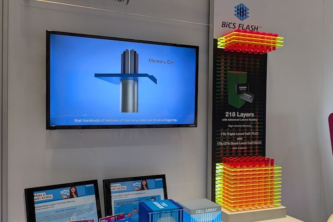
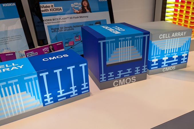
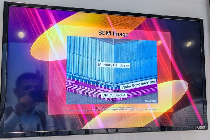

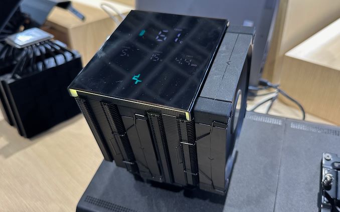
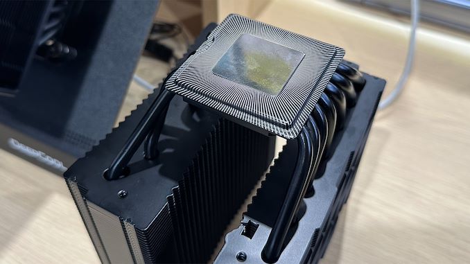
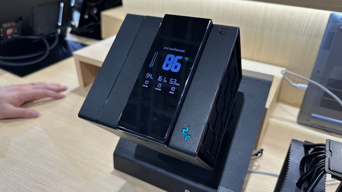
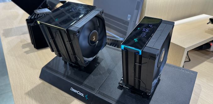
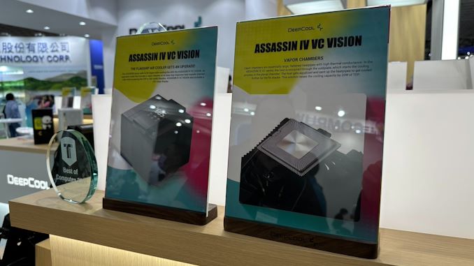
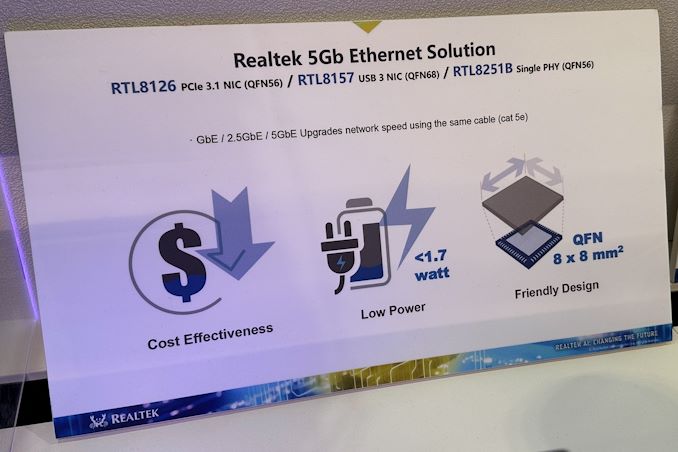
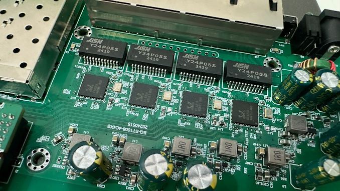
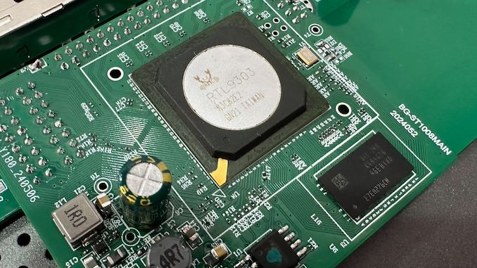
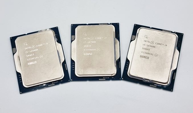




0 Comments