Antec's 'Performance 1M' Mini-ITX Chassis Can House a GeForce RTX 4090 <p align="center"><a href="https://www.anandtech.com/show/21443/antecs-miniitx-chassis-can-house-a-geforce-rtx-4090"><img src="https://images.anandtech.com/doci/21443/IMG_0852-678_575px.jpg" alt="" /></a></p><p><p>With the highly integrated nature of PCs these days, the Mini-ITX form-factor has become a very viable option for high-performance gaming system. With plenty of motherboards available for both AMD and Intel's latest platforms, equipping an ITX system with a CPU is easy enough. But the small size of the form factor means that housing an ultra-wide flagship-level graphics card remains an issue. For this year's Computex trade show, Antec was showing off their solution to the problem of giant video cards: the Performance 1M case, a Mini-ITX case with a separate chamber just for a large video card.</p>
<p style="text-align: center;"><a href="https://www.anandtech.com/show/21443/antecs-miniitx-chassis-can-house-a-geforce-rtx-4090"><img alt="" src="https://images.anandtech.com/doci/21443/IMG_0856-25x16_575px.jpg" /></a></p>
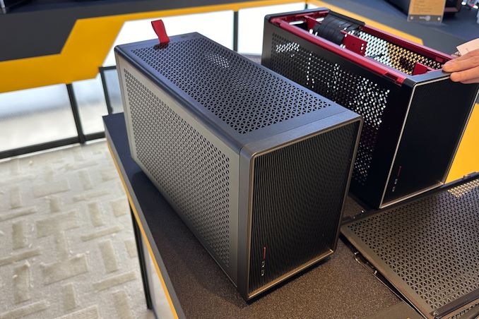
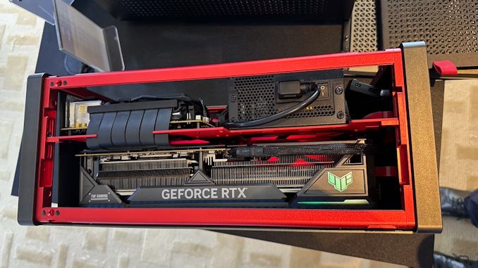
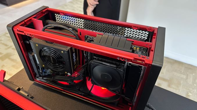
<p>Antec's Performance 1M is a dual-chamber Mini-ITX chassis that splits off the video card from the rest of the system. The primary chamber houses a Mini-ITX motherboard and an SFX power supply, while the secondary chamber houses a huge graphics card. Notably, the two chambers are bridged using a PCIe riser cable, allowing the motherboard chamber to be far shorter than even a half-height PCIe card, while the video card chamber can hold a triple-slot video card parallel to the motherboard chamber, cutting down on wasted space. For Antec's Computex demo, the company had a triple-slot ASUS GeForce RTX 4090 installed to showcase how this worked.</p>
<p style="text-align: center;"><a href="https://www.anandtech.com/show/21443/antecs-miniitx-chassis-can-house-a-geforce-rtx-4090"><img alt="" src="https://images.anandtech.com/doci/21443/IMG_0844_575px.jpg" /></a></p>
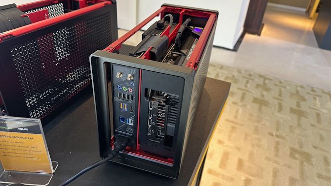
<p>Antec's decision to allocate most of the case's volume to th video card chamber does come with a slight catch, however: it doesn't leave much space for a CPU cooler in the motherboard chamber. The short motherboard chamber means that system builders will have to use a low-profile cooler; these are readily available, but it does leave less thermal headroom overall for high-end CPUs. So there are still trade-offs for being able to accommodate a high-end video card.</p>
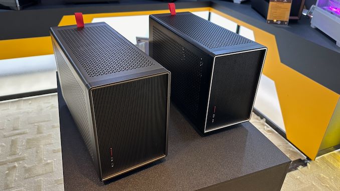
<p>Otherwise, the Performance 1M chassis from Antec look very stylish and are traditionally well built from stainless steel and aluminum. The chassis can be equipped with two 120-mm or two 140-mm coolers for extra airflow (which will help performance), one 2.5-inch SATA SSD, and even some RGB bling. To make the PC built inside a Performance 1M case more convenient to use, there are two USB Type-C ports on the front.</p>
<p><a href="https://www.anandtech.com/show/21443/antecs-miniitx-chassis-can-house-a-geforce-rtx-4090"><img alt="" src="https://images.anandtech.com/doci/21443/IMG_0846_575px.jpg" /></a></p>
<p>Of course, housing a GeForce RTX 4090 graphics card in a Mini-ITX chassis has its peculiarities when it comes to dimensions and Antec's Performance 1M measures 424×175×260mm, which is pretty large. On the other hand, for an ultra-high-performance gaming system, this is pretty compact.</p>
<p style="text-align: center;"><a href="https://www.anandtech.com/show/21443/antecs-miniitx-chassis-can-house-a-geforce-rtx-4090"><img alt="" src="https://images.anandtech.com/doci/21443/IMG_0850_575px.jpg" /></a></p>
<p>Antec's Performance 1M Mini-ITX chassis will be available in gunmetal gray and matte black colors sometimes later this year. Pricing is something that the company is thinking about now, though keep in mind that we are talking about unique premium products.</p>
</p> Cases/Cooling/PSUs
Antec's 'Performance 1M' Mini-ITX Chassis Can House a GeForce RTX 4090
With the highly integrated nature of PCs these days, the Mini-ITX form-factor has become a very viable option for high-performance gaming system. With plenty of motherboards available for both AMD and Intel's latest platforms, equipping an ITX system with a CPU is easy enough. But the small size of the form factor means that housing an ultra-wide flagship-level graphics card remains an issue. For this year's Computex trade show, Antec was showing off their solution to the problem of giant video cards: the Performance 1M case, a Mini-ITX case with a separate chamber just for a large video card.
Antec's Performance 1M is a dual-chamber Mini-ITX chassis that splits off the video card from the rest of the system. The primary chamber houses a Mini-ITX motherboard and an SFX power supply, while the secondary chamber houses a huge graphics card. Notably, the two chambers are bridged using a PCIe riser cable, allowing the motherboard chamber to be far shorter than even a half-height PCIe card, while the video card chamber can hold a triple-slot video card parallel to the motherboard chamber, cutting down on wasted space. For Antec's Computex demo, the company had a triple-slot ASUS GeForce RTX 4090 installed to showcase how this worked.
Antec's decision to allocate most of the case's volume to th video card chamber does come with a slight catch, however: it doesn't leave much space for a CPU cooler in the motherboard chamber. The short motherboard chamber means that system builders will have to use a low-profile cooler; these are readily available, but it does leave less thermal headroom overall for high-end CPUs. So there are still trade-offs for being able to accommodate a high-end video card.
Otherwise, the Performance 1M chassis from Antec look very stylish and are traditionally well built from stainless steel and aluminum. The chassis can be equipped with two 120-mm or two 140-mm coolers for extra airflow (which will help performance), one 2.5-inch SATA SSD, and even some RGB bling. To make the PC built inside a Performance 1M case more convenient to use, there are two USB Type-C ports on the front.
Of course, housing a GeForce RTX 4090 graphics card in a Mini-ITX chassis has its peculiarities when it comes to dimensions and Antec's Performance 1M measures 424×175×260mm, which is pretty large. On the other hand, for an ultra-high-performance gaming system, this is pretty compact.
Antec's Performance 1M Mini-ITX chassis will be available in gunmetal gray and matte black colors sometimes later this year. Pricing is something that the company is thinking about now, though keep in mind that we are talking about unique premium products.


, one 2.5-inch SATA SSD, and even some RGB bling. To make the PC built inside a Performance 1M case more convenient to use, there are two USB Type-C ports on the front.</p>
<p><a href="https://www.anandtech.com/show/21443/antecs-miniitx-chassis-can-house-a-geforce-rtx-4090"><img alt="" src="https://images.anandtech.com/doci/21443/IMG_0846_575px.jpg" /></a></p>
<p>Of course, housing a GeForce RTX 4090 graphics card in a Mini-ITX chassis has its peculiarities when it comes to dimensions and Antec's Performance 1M measures 424×175×260mm, which is pretty large. On the other hand, for an ultra-high-performance gaming system, this is pretty compact.</p>
<p style="text-align: center;"><a href="https://www.anandtech.com/show/21443/antecs-miniitx-chassis-can-house-a-geforce-rtx-4090"><img alt="" src="https://images.anandtech.com/doci/21443/IMG_0850_575px.jpg" /></a></p>
<p>Antec's Performance 1M Mini-ITX chassis will be available in gunmetal gray and matte black colors sometimes later this year. Pricing is something that the company is thinking about now, though keep in mind that we are talking about unique premium products.</p>
</p> Cases/Cooling/PSUs)
, one 2.5-inch SATA SSD, and even some RGB bling. To make the PC built inside a Performance 1M case more convenient to use, there are two USB Type-C ports on the front.</p>
<p><a href="https://www.anandtech.com/show/21443/antecs-miniitx-chassis-can-house-a-geforce-rtx-4090"><img alt="" src="https://images.anandtech.com/doci/21443/IMG_0846_575px.jpg" /></a></p>
<p>Of course, housing a GeForce RTX 4090 graphics card in a Mini-ITX chassis has its peculiarities when it comes to dimensions and Antec's Performance 1M measures 424×175×260mm, which is pretty large. On the other hand, for an ultra-high-performance gaming system, this is pretty compact.</p>
<p style="text-align: center;"><a href="https://www.anandtech.com/show/21443/antecs-miniitx-chassis-can-house-a-geforce-rtx-4090"><img alt="" src="https://images.anandtech.com/doci/21443/IMG_0850_575px.jpg" /></a></p>
<p>Antec's Performance 1M Mini-ITX chassis will be available in gunmetal gray and matte black colors sometimes later this year. Pricing is something that the company is thinking about now, though keep in mind that we are talking about unique premium products.</p>
</p> Cases/Cooling/PSUs | https://compbuddey.blogspot.com/2024/06/antecs-performance-1m-mini-itx-chassis_30.html)
, one 2.5-inch SATA SSD, and even some RGB bling. To make the PC built inside a Performance 1M case more convenient to use, there are two USB Type-C ports on the front.</p>
<p><a href="https://www.anandtech.com/show/21443/antecs-miniitx-chassis-can-house-a-geforce-rtx-4090"><img alt="" src="https://images.anandtech.com/doci/21443/IMG_0846_575px.jpg" /></a></p>
<p>Of course, housing a GeForce RTX 4090 graphics card in a Mini-ITX chassis has its peculiarities when it comes to dimensions and Antec's Performance 1M measures 424×175×260mm, which is pretty large. On the other hand, for an ultra-high-performance gaming system, this is pretty compact.</p>
<p style="text-align: center;"><a href="https://www.anandtech.com/show/21443/antecs-miniitx-chassis-can-house-a-geforce-rtx-4090"><img alt="" src="https://images.anandtech.com/doci/21443/IMG_0850_575px.jpg" /></a></p>
<p>Antec's Performance 1M Mini-ITX chassis will be available in gunmetal gray and matte black colors sometimes later this year. Pricing is something that the company is thinking about now, though keep in mind that we are talking about unique premium products.</p>
</p> Cases/Cooling/PSUs&body=https://compbuddey.blogspot.com/2024/06/antecs-performance-1m-mini-itx-chassis_30.html)
0 Comments