
AMD Announces The Ryzen AI 300 Series For Mobile: Zen 5 With RDNA 3.5, and XDNA2 NPU With 50 TOPS
During AMD's opening keynote at Computex 2024, company CEO Dr. Lisa Su revealed AMD's latest AI PC-focused chip lineup for the mobile market, the Ryzen AI 300 series. Based on AMD's new Zen 5 CPU microarchitecture, the Ryzen AI 300 series – codenamed Strix Point – is intended to offer an across-the-board improvement in mobile SoC performance, with AMD proclaiming that the Ryzen AI 300 series will offer the fastest AI inference performance within the compact and portable PC market.
Under the hood, the new mobile SoC from AMD incorporates not only their new Zen 5 CPU architecture, but also their new RDNA 3.5-based integrated graphics, and the third generation XDNA2-based NPU, the latter of which is rated to deliver 50 TOPS of performance for AI-based workloads. As a result, the Ryzen AI 300 series represents a significant upgrade in AMD's mobile chip lineup, with all of the major aspects of the platform receiving a major upgrade versus their Zen 4-era Phoenix/Hawk Point SoCs. The one thing the new platform won't get, however, is a process node improvement; AMD is building Strix Point on a 4nm node, just like Phoenix/Hawk Point before it.
For this morning's announcement, AMD has unveiled the first two Ryzen AI 300 SKUs designed for notebooks. The first of these is the Ryzen AI 9 HX 370, which features 12 Zen 5 cores with a maximum boost frequency of up to 5.1 GHz, and comes equipped with 36 MB cache (12 MB L2 + 24 MB L3). The other chip to be announced is the Ryzen AI 9 365, which has two fewer Zen 5 cores (10 cores) and operates with a 5,0 GHz boost frequency and a 10 MB L2 + 24 MB L3 cache allocation.
CPUs
Posted by The Techinical Support

TSMC: Performance and Yields of 2nm on Track, Mass Production To Start In 2025 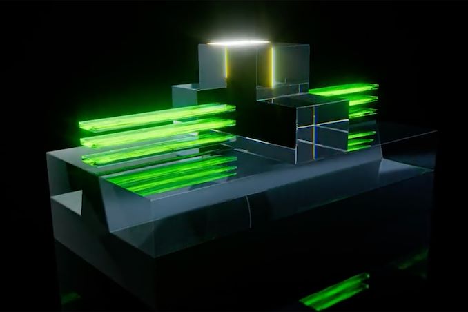
In addition to revealing its roadmap and plans concerning its current leading-edge process technologies, TSMC also shared progress of its N2 node as part of its Symposiums 2024. The company's first 2nm-class fabrication node, and predominantly featuring gate-all-around transistors, according to TSMC N2 has almost achieved its target performance and yield goals, which places it on track to enter high-volume manufacturing in the second half of 2025.
TSMC states that 'N2 development is well on track and N2P is next.' In particular, gate-all-around nanosheet devices currently achieve over 90% of their expected performance, whereas yields of 256 Mb SRAM (32 MB) devices already exceeds 80%, depending on the batch. All of this for a node that is over a year away from mass production.
Meanwhile, average yield of a 256 Mb SRAM was around 70% as of March, 2024, up from around 35% in April, 2023. Device performance has also been improving with higher frequencies being achieved while keeping power consumption in check.
Chip designer interest towards TSMC's first 2nm-class gate-all-around nanosheet transistor-based technology is significant, too. The number of new tape-outs (NTOs) in the first year of N2 is over two-times higher than it was for N5. Though with that said, given TSMC's close working relationship with a handful of high-volume vendors – most notably Appe – NTOs can be a very misleading figure since the first year of a new node at TSMC is capacity constrained, and consequently the bulk of that capacity goes to TSMC's priority partners.
Meanwhile, there were considerably more N5 tapeouts in its second year (some where N5P, of course) and N2 promises to have 2.6X more NTOs in its second year. So the node indeed looks quite promising. In fact, based on TSMC's slides (which we're unfortunately not able to republish), N2 is more popular than N3 in terms of NTOs both in the first and the second years of existence.
When it comes to the second year of N2, in the second half of 2026 TSMC plans to roll out its N2P technology, which promises additional performance and power benefits. N2P is expected to improve frequency by 15% - 20%, reduce power consumption by 30% - 40%, and increase chip density by over 1.15 times compared to N3E, significant benefits to move to all-new GAA nanosheet transistors.
Finally, for those companies that need the best in performance, power, and density, TSMC is poised to offer their A16 process in 2026. That node will also bring in backside power delivery, which will add costs, but is expected to greatly improve performance efficiency and scaling.
Semiconductors

Samsung Foundry Unveils Updated Roadmap: BSPDN and 2nm Evolution Through 2027 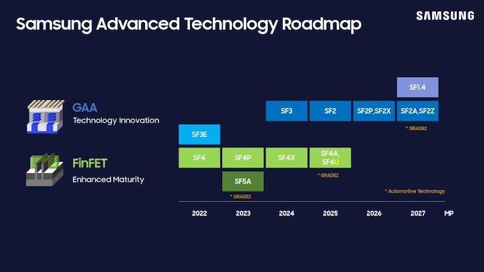
Samsung this week has unveiled its latest process technologies roadmap at the company's Samsung Foundry Forum (SFF) U.S. The new plan covers the evolution of Samsung's 2nm-class production nodes through 2027, including a process technology with a backside power delivery, re-emphasizing plans to bring out a 1.4nm-class node in 2027, and the introduction of a 'high value' 4nm-class manufacturing tech.
Samsung Foundry's key announcements for today are clearly focused on the its 2nm-class process technologies, which are set to enter production in 2025 and will span to 2027, when the company's 1.4-nm class production node is set to enter the scene. Samsung is also adding (or rather, renaming) another 2nm-class node to their roadmap with SF2, which was previously disclosed by Samsung as SF3P and aimed at high-performance devices.
"We have refined and improved the SF3P, resulting in what we now refer to as SF2," a Samsung spokesperson told AnandTech. "This enhanced node incorporates various process design improvements, delivering notable power, performance, and area (PPA) benefits."
| Samsung Foundry for Leading-Edge Nodes Announced on June 12, 2024 Compiled by AnandTech |
||||||||
| HVM Start | 2023 | 2024 | 2025 | 2026 | 2027 | 2027 | ||
| Process | SF3E | SF3 | SF2 (aka SF3P) |
SF2P/SF2X | SF2Z | SF1.4 | ||
| FET | GAAFET | |||||||
| Power Delivery | Frontside | Backside (BSPDN) | ? | |||||
| EUV | 0.33 NA EUV | ? | ? | ? | ? | |||
This is another example of a rebranding of leading-edge fabrication nodes in the recent years by a major chipmaker. Samsung Foundry is not disclosing any specific PPA improvements SF3P has over SF2, and for now is only stating in high-level terms that it will be a better-performing node than the planned SF3P.
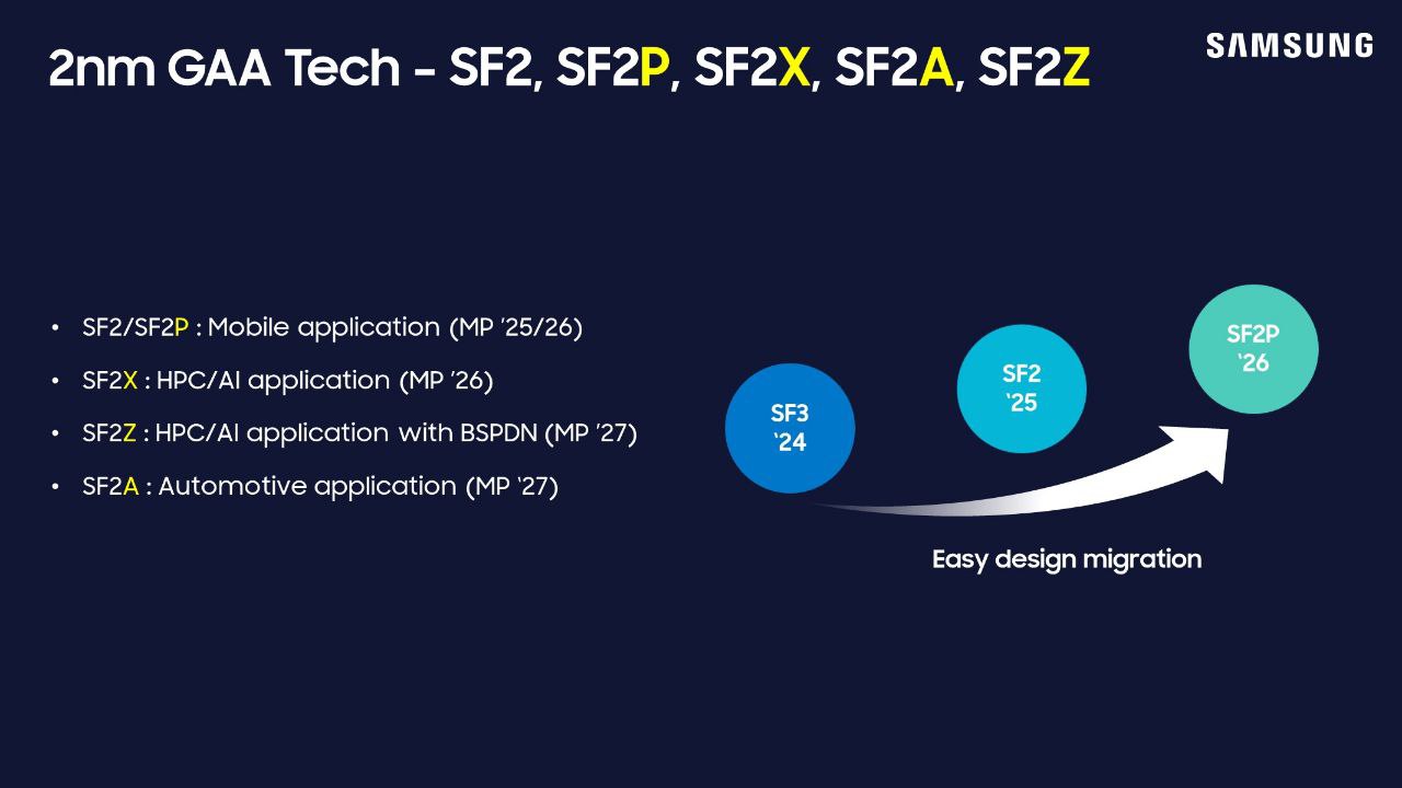
Meanwhile, this week's announcement also includes new information on Samsung's next batch of process nodes, which are planned for 2026 and 2027. In 2026 Samsung will have SF2P, a further refinement of SF2 which incorporates 'faster' yet less dense transistors. That will be followed up in 2027 with SF2Z, which adds backside power delivery to the mix for better and higher quality power delivery. In particular, Samsung is targetting voltate drop (aka IR drop) here, which is an ongoing concern in chip design.
Finally, SF1.4, a 1.4nm-class node, is on track for 2027 as well. Interestingly, however, it looks like it does not feature a backside power delivery. Which, per current roadmaps, would have Samsung as the only foundry not using BSPDN for their first 1.4nm/14Å-class node.
"We have optimized BSPDN and incorporated it for the first time in the SF2Z node we announced today," the spokesperso... Semiconductors

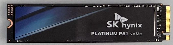
SK hynix Platinum P51 Gen5 SSD with 238L NAND Spotted at GTC 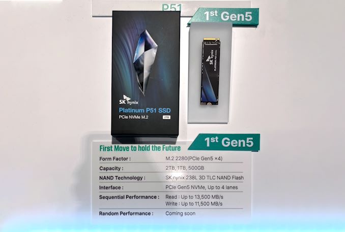
SK hynix is set to unveil their first Gen5 consumer NVMe SSD lineup shortly, based on the products at display in their GTC 2024 booth. The Platinum P51 M.2 2280 NVMe SSD will take over flagship duties from the Platinum P41 that has been serving the market for more than a year.
Similar to the Gold P31 and the Platinum P41, the Platinum P51 also uses an in-house SSD controller. The key updates are the move to PCIe Gen5 and the use of SK hynix's 238L TLC NAND. Other details are scarce, and we have reached out for additional information.
| SK hynix Platinum P51 Gen5 NVMe SSD Specifications | ||||
| Capacity | 500 GB | 1 TB | 2 TB | |
| Controller | SK hynix In-House (Alistar) | |||
| NAND Flash | SK hynix 238L 3D TLC NAND at ?? MT/s ('4D' with CMOS circuitry under the NAND as per SK hynix marketing) | |||
| Form-Factor, Interface | M.2-2280, PCIe 5.0 x4, NVMe 2.0 | |||
| Sequential Read | 13500 MB/s | |||
| Sequential Write | 11500 MB/s | |||
| Random Read IOPS | TBD | |||
| Random Write IOPS | TBD | |||
| SLC Caching | Yes | |||
| TCG Opal Encryption | TBD | |||
| Warranty | TBD | |||
| Write Endurance | TBD | TBD | TBD | |
Only the peak sequential access numbers were available at the GTC booth, indicating that the drive's firmware is still undergoing tweaks. It is also unclear how these numbers are going to vary based on capacity. Availability and pricing are also not public yet.
This is a significant launch for the Gen5 consumer SSD market, where the number of available options are quite limited. The Phison E26 controller and Micron's B58R NAND combination is already in its second generation (with the NAND operating at 2400 MT/s in the newest avatar), but other vertically integrated vendors such as Samsung, Western Digital / Kioxia, and SK hynix (till now) are focusing more on the Gen4 market which has much higher adoption.
We will update the piece with additional information once the specifications are officially available.
Storage
TSMC's Roadmap at a Glance: N3X, N2P, A16 Coming in 2025/2026 
As announced last week by TSMC, later this year the company is set to start high-volume manufacturing on its N3P fabrication process, and this will be the company's most advanced node for a while. Next year things will get a bit more interesting as TSMC will have two process technologies that could actually compete against each other when they enter high-volume manufacturing (HVM) in the second half of 2025.
| Advertised PPA Improvements of New Process Technologies Data announced during conference calls, events, press briefings and press releases |
|||||||||
| Compiled by AnandTech |
TSMC | ||||||||
| N3 vs N5 |
N3E vs N5 |
N3P vs N3E |
N3X vs N3P |
N2 vs N3E |
N2P vs N3E |
N2P vs N2 |
A16 vs N2P |
||
| Power | -25% -30% |
-34% | -5% -10% |
-7%*** | -25% -30% |
-30% -40% |
-5% -10% |
-15% -20% |
|
| Performance | +10% +15% |
+18% | +5% | +5% Fmax @1.2V** |
+10% +15% |
+15% +20% |
+5 +10% |
+8% +10% |
|
| Density* | ? | 1.3x | 1.04x | 1.10x*** | 1.15x | 1.15x | ? | 1.07x 1.10x |
|
| HVM | Q4 2022 |
Q4 2023 |
H2 2024 |
H2 2025 |
H2 2025 |
H2 2026 |
H2 2026 |
H2 2026 |
|
*Chip density published by TSMC reflects 'mixed' chip density consisting of 50% logic, 30% SRAM, and 20% analog.
**At the same area.
***At the same speed.
The production nodes are N3X (3nm-class, extreme performance-focused) as well as N2 (2nm-class). TSMC says that when compared to N3P, chips made on N3X can either lower power consumption by 7% at the same frequency by lowering Vdd from 1.0V to 0.9V, increase performance by 5% at the same area, or increase transistor density by around 10% at the same frequency. Meanwhile, the key advantage of N3X compared to predecessors is its maximum voltage of 1.2V, which is important for ultra-high-performance applications, such as desktop or datacenter GPUs.
TSMC's N2 will be TSMC's first production node to use gate-all-around (GAA) nanosheet transistors and this will significantly enhance its performance, power, and are... Semiconductors
TSMC: Performance and Yields of 2nm on Track, Mass Production To Start In 2025
In addition to revealing its roadmap and plans concerning its current leading-edge process technologies, TSMC also shared progress of its N2 node as part of its Symposiums 2024. The company's first 2nm-class fabrication node, and predominantly featuring gate-all-around transistors, according to TSMC N2 has almost achieved its target performance and yield goals, which places it on track to enter high-volume manufacturing in the second half of 2025.
TSMC states that 'N2 development is well on track and N2P is next.' In particular, gate-all-around nanosheet devices currently achieve over 90% of their expected performance, whereas yields of 256 Mb SRAM (32 MB) devices already exceeds 80%, depending on the batch. All of this for a node that is over a year away from mass production.
Meanwhile, average yield of a 256 Mb SRAM was around 70% as of March, 2024, up from around 35% in April, 2023. Device performance has also been improving with higher frequencies being achieved while keeping power consumption in check.
Chip designer interest towards TSMC's first 2nm-class gate-all-around nanosheet transistor-based technology is significant, too. The number of new tape-outs (NTOs) in the first year of N2 is over two-times higher than it was for N5. Though with that said, given TSMC's close working relationship with a handful of high-volume vendors – most notably Appe – NTOs can be a very misleading figure since the first year of a new node at TSMC is capacity constrained, and consequently the bulk of that capacity goes to TSMC's priority partners.
Meanwhile, there were considerably more N5 tapeouts in its second year (some where N5P, of course) and N2 promises to have 2.6X more NTOs in its second year. So the node indeed looks quite promising. In fact, based on TSMC's slides (which we're unfortunately not able to republish), N2 is more popular than N3 in terms of NTOs both in the first and the second years of existence.
When it comes to the second year of N2, in the second half of 2026 TSMC plans to roll out its N2P technology, which promises additional performance and power benefits. N2P is expected to improve frequency by 15% - 20%, reduce power consumption by 30% - 40%, and increase chip density by over 1.15 times compared to N3E, significant benefits to move to all-new GAA nanosheet transistors.
Finally, for those companies that need the best in performance, power, and density, TSMC is poised to offer their A16 process in 2026. That node will also bring in backside power delivery, which will add costs, but is expected to greatly improve performance efficiency and scaling.
Semiconductors
Samsung Foundry Unveils Updated Roadmap: BSPDN and 2nm Evolution Through 2027
Samsung this week has unveiled its latest process technologies roadmap at the company's Samsung Foundry Forum (SFF) U.S. The new plan covers the evolution of Samsung's 2nm-class production nodes through 2027, including a process technology with a backside power delivery, re-emphasizing plans to bring out a 1.4nm-class node in 2027, and the introduction of a 'high value' 4nm-class manufacturing tech.
Samsung Foundry's key announcements for today are clearly focused on the its 2nm-class process technologies, which are set to enter production in 2025 and will span to 2027, when the company's 1.4-nm class production node is set to enter the scene. Samsung is also adding (or rather, renaming) another 2nm-class node to their roadmap with SF2, which was previously disclosed by Samsung as SF3P and aimed at high-performance devices.
"We have refined and improved the SF3P, resulting in what we now refer to as SF2," a Samsung spokesperson told AnandTech. "This enhanced node incorporates various process design improvements, delivering notable power, performance, and area (PPA) benefits."
| Samsung Foundry for Leading-Edge Nodes Announced on June 12, 2024 Compiled by AnandTech |
||||||||
| HVM Start | 2023 | 2024 | 2025 | 2026 | 2027 | 2027 | ||
| Process | SF3E | SF3 | SF2 (aka SF3P) |
SF2P/SF2X | SF2Z | SF1.4 | ||
| FET | GAAFET | |||||||
| Power Delivery | Frontside | Backside (BSPDN) | ? | |||||
| EUV | 0.33 NA EUV | ? | ? | ? | ? | |||
This is another example of a rebranding of leading-edge fabrication nodes in the recent years by a major chipmaker. Samsung Foundry is not disclosing any specific PPA improvements SF3P has over SF2, and for now is only stating in high-level terms that it will be a better-performing node than the planned SF3P.
Meanwhile, this week's announcement also includes new information on Samsung's next batch of process nodes, which are planned for 2026 and 2027. In 2026 Samsung will have SF2P, a further refinement of SF2 which incorporates 'faster' yet less dense transistors. That will be followed up in 2027 with SF2Z, which adds backside power delivery to the mix for better and higher quality power delivery. In particular, Samsung is targetting voltate drop (aka IR drop) here, which is an ongoing concern in chip design.
Finally, SF1.4, a 1.4nm-class node, is on track for 2027 as well. Interestingly, however, it looks like it does not feature a backside power delivery. Which, per current roadmaps, would have Samsung as the only foundry not using BSPDN for their first 1.4nm/14Å-class node.
"We have optimized BSPDN and incorporated it for the first time in the SF2Z node we announced today," the spokesperso... Semiconductors
SK hynix Platinum P51 Gen5 SSD with 238L NAND Spotted at GTC
SK hynix is set to unveil their first Gen5 consumer NVMe SSD lineup shortly, based on the products at display in their GTC 2024 booth. The Platinum P51 M.2 2280 NVMe SSD will take over flagship duties from the Platinum P41 that has been serving the market for more than a year.
Similar to the Gold P31 and the Platinum P41, the Platinum P51 also uses an in-house SSD controller. The key updates are the move to PCIe Gen5 and the use of SK hynix's 238L TLC NAND. Other details are scarce, and we have reached out for additional information.
| SK hynix Platinum P51 Gen5 NVMe SSD Specifications | ||||
| Capacity | 500 GB | 1 TB | 2 TB | |
| Controller | SK hynix In-House (Alistar) | |||
| NAND Flash | SK hynix 238L 3D TLC NAND at ?? MT/s ('4D' with CMOS circuitry under the NAND as per SK hynix marketing) | |||
| Form-Factor, Interface | M.2-2280, PCIe 5.0 x4, NVMe 2.0 | |||
| Sequential Read | 13500 MB/s | |||
| Sequential Write | 11500 MB/s | |||
| Random Read IOPS | TBD | |||
| Random Write IOPS | TBD | |||
| SLC Caching | Yes | |||
| TCG Opal Encryption | TBD | |||
| Warranty | TBD | |||
| Write Endurance | TBD | TBD | TBD | |
Only the peak sequential access numbers were available at the GTC booth, indicating that the drive's firmware is still undergoing tweaks. It is also unclear how these numbers are going to vary based on capacity. Availability and pricing are also not public yet.
This is a significant launch for the Gen5 consumer SSD market, where the number of available options are quite limited. The Phison E26 controller and Micron's B58R NAND combination is already in its second generation (with the NAND operating at 2400 MT/s in the newest avatar), but other vertically integrated vendors such as Samsung, Western Digital / Kioxia, and SK hynix (till now) are focusing more on the Gen4 market which has much higher adoption.
We will update the piece with additional information once the specifications are officially available.
Storage
TSMC's Roadmap at a Glance: N3X, N2P, A16 Coming in 2025/2026
As announced last week by TSMC, later this year the company is set to start high-volume manufacturing on its N3P fabrication process, and this will be the company's most advanced node for a while. Next year things will get a bit more interesting as TSMC will have two process technologies that could actually compete against each other when they enter high-volume manufacturing (HVM) in the second half of 2025.
| Advertised PPA Improvements of New Process Technologies Data announced during conference calls, events, press briefings and press releases |
|||||||||
| Compiled by AnandTech |
TSMC | ||||||||
| N3 vs N5 |
N3E vs N5 |
N3P vs N3E |
N3X vs N3P |
N2 vs N3E |
N2P vs N3E |
N2P vs N2 |
A16 vs N2P |
||
| Power | -25% -30% |
-34% | -5% -10% |
-7%*** | -25% -30% |
-30% -40% |
-5% -10% |
-15% -20% |
|
| Performance | +10% +15% |
+18% | +5% | +5% Fmax @1.2V** |
+10% +15% |
+15% +20% |
+5 +10% |
+8% +10% |
|
| Density* | ? | 1.3x | 1.04x | 1.10x*** | 1.15x | 1.15x | ? | 1.07x 1.10x |
|
| HVM | Q4 2022 |
Q4 2023 |
H2 2024 |
H2 2025 |
H2 2025 |
H2 2026 |
H2 2026 |
H2 2026 |
|
*Chip density published by TSMC reflects 'mixed' chip density consisting of 50% logic, 30% SRAM, and 20% analog.
**At the same area.
***At the same speed.
The production nodes are N3X (3nm-class, extreme performance-focused) as well as N2 (2nm-class). TSMC says that when compared to N3P, chips made on N3X can either lower power consumption by 7% at the same frequency by lowering Vdd from 1.0V to 0.9V, increase performance by 5% at the same area, or increase transistor density by around 10% at the same frequency. Meanwhile, the key advantage of N3X compared to predecessors is its maximum voltage of 1.2V, which is important for ultra-high-performance applications, such as desktop or datacenter GPUs.
TSMC's N2 will be TSMC's first production node to use gate-all-around (GAA) nanosheet transistors and this will significantly enhance its performance, power, and are... Semiconductors




The AMD Computex 2024 Keynote Live Blog (6:30pm PT/01:30 UTC) Computex keynote season is kicking into high gear this morning with the show's leading keynote, which is being delivered by AMD. Company CEO Dr. Lisa Su will be presenting a keynote entitled “The future of high-performance computing in the AI era,” and with a run time of 90 minutes, we're expecting AMD to have a whole host of product announcements covering their full spectrum of product categories.
The big expectation here is fresh news around AMD’s Zen 5 CPU core architecture, and the chips built around it. AMD’s most recent Zen 5 roadmap has it slated to deliver all three flavors of Zen 5 by the end of this year, and we’re coming up on the two-year anniversary of the Zen 4 architecture launch.
Along with client chips, AMD has been pushing their server CPUs hard, and they’ve previously told investors that the next-gen EPYC Turin CPU is “looking great”. So we’ll likely hear about both client and server Zen 5 product plans during this keynote.
On the GPU/accelerator side of matters, AMD is mid-cycle (at best) with their Instinct MI300 series accelerators. With the company’s sales repeatedly beating their own expectations, AMD doesn’t seem to need much help moving this premium silicon right now. But with AI being the operative buzzword of this year’s Computex (and indeed, the computing industry as a whole), it would be weird for AMD to not have something to say about their rapidly growing AI accelerator product line.
Come join us at 6:30pm PT / 9:30pm ET / 01:30 UTC to get all the details.
Live Blog

SK hynix Wraps up Dev Work on High-End PCB01 PCIe 5.0 SSD for OEMs, Launching Later This Year 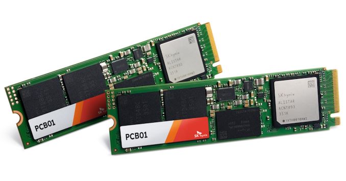
SK hynix early in Friday announced that the company has finished the development of it's PCB01 PCIe Gen5 SSD, the company's forthcoming high-end SSD for OEMs. Based on the company's new Alistar platform, the PCB01 is designed to deliver chart-topping performance for client machines. And, as a sign of the times, SK hynix is positioning the PCB01 for AI PCs, looking to synergize with the overall industry interest in anything and everything AI.
The bare, OEM-focused drives have previously been shown off by SK hynix, and make no attempt to hide what's under the hood. The PCB01 relies on SK hynix's Alistar controller, which features a PCIe Gen5 x4 host interface on the front end and eight NAND channels on the back end, placing it solidly in the realm of high-end SSDs. Paired with the Alistar controller is the company's latest 238-layer TLC NAND (H25T1TD48C & H25T2TD88C), which offers a maximum transfer speed of 2400 MT/second. Being that this is a high-end client SSD, there's also a DRAM chip on board, though the company isn't disclosing its capacity.
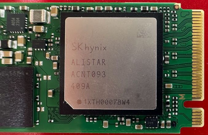
As with other high-end PCIe 5.0 client SSDs, SK hynix is planning on hitting peak read speeds of up to 14GB/second on the drive, while peak sequential write speeds should top 12GB/second (with pSLC caching, of course) – performance figures well within the realm of possibility for an 8 channel drive. As for random performance, at Computex the company was telling attendees that the drives should be able to sustain 4K random read and write rates of 2 million IOPS, which is very high as well. The SSDs are also said to consume up to 30% less power than 'predecessors,' according to SK hynix, though the company didn't elaborate on that figure. Typically in the storage industry, energy figures are based on iso-performance (rather than peak performance) – essentially measuring energy efficiency per bit rather than toal power consumption – and that is likely the case here as well.
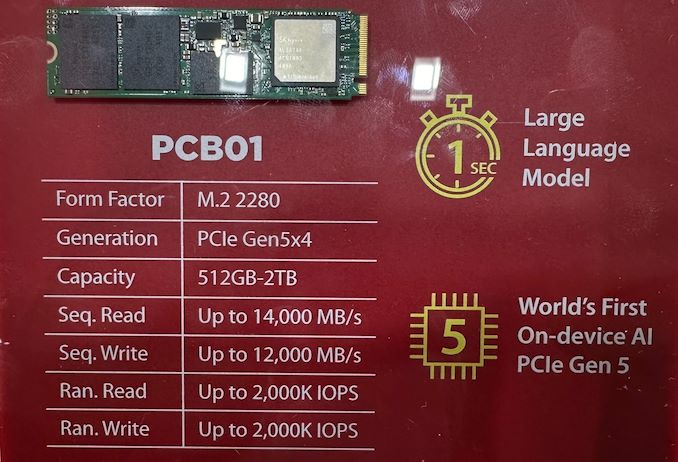
At least initially, SK Hynix plans to release its PCB01 in three capacities – 512 GB, 1 TB, and 2 TB. The company has previously disclosed that their 238L TLC NAND has a capacity of 512Gbit, so these are typical capacity figures for single-sided drives. And while the focus of the company's press release this week was on OEM drives, this is the same controller and NAND that is also going into the company's previously-teased retail Platinum P51 SSD, so this week's reveal offers a bit more detail into what to expect from that drive family as well.
Specs aside, Ahn Hyun, the Head of the N-S Committee at SK hynix, said that multiple global CPU providers for on-device AI PCs are seeking collaboration for the compatibility validation process, which is underway, so expect PCB01 drives inside PCs in this back-to-school and holiday seasons.
"We will work towards enhancing our leadership as the global top AI memory provider also in the NAND solution space by successfully completing the customer validation and mass production of PCB01, which will be in the limelight," Ahn Hyun said.
SSDs



Lorem Ipsum is simply dummy text of the printing and typesetting industry. Lorem Ipsum has been the industry's.
TSMC: Performance and Yields of 2nm on Track, Mass Production To Start In 2025
In addition to revealing its roadmap and plans concerning its current leading-edge process technologies, TSMC also shared progress of its N2 node as part of its Symposiums 2024. The company's first 2nm-class fabrication node, and predominantly featuring gate-all-around transistors, according to TSMC N2 has almost achieved its target performance and yield goals, which places it on track to enter high-volume manufacturing in the second half of 2025.
TSMC states that 'N2 development is well on track and N2P is next.' In particular, gate-all-around nanosheet devices currently achieve over 90% of their expected performance, whereas yields of 256 Mb SRAM (32 MB) devices already exceeds 80%, depending on the batch. All of this for a node that is over a year away from mass production.
Meanwhile, average yield of a 256 Mb SRAM was around 70% as of March, 2024, up from around 35% in April, 2023. Device performance has also been improving with higher frequencies being achieved while keeping power consumption in check.
Chip designer interest towards TSMC's first 2nm-class gate-all-around nanosheet transistor-based technology is significant, too. The number of new tape-outs (NTOs) in the first year of N2 is over two-times higher than it was for N5. Though with that said, given TSMC's close working relationship with a handful of high-volume vendors – most notably Appe – NTOs can be a very misleading figure since the first year of a new node at TSMC is capacity constrained, and consequently the bulk of that capacity goes to TSMC's priority partners.
Meanwhile, there were considerably more N5 tapeouts in its second year (some where N5P, of course) and N2 promises to have 2.6X more NTOs in its second year. So the node indeed looks quite promising. In fact, based on TSMC's slides (which we're unfortunately not able to republish), N2 is more popular than N3 in terms of NTOs both in the first and the second years of existence.
When it comes to the second year of N2, in the second half of 2026 TSMC plans to roll out its N2P technology, which promises additional performance and power benefits. N2P is expected to improve frequency by 15% - 20%, reduce power consumption by 30% - 40%, and increase chip density by over 1.15 times compared to N3E, significant benefits to move to all-new GAA nanosheet transistors.
Finally, for those companies that need the best in performance, power, and density, TSMC is poised to offer their A16 process in 2026. That node will also bring in backside power delivery, which will add costs, but is expected to greatly improve performance efficiency and scaling.
Semiconductors
Samsung Foundry Unveils Updated Roadmap: BSPDN and 2nm Evolution Through 2027
Samsung this week has unveiled its latest process technologies roadmap at the company's Samsung Foundry Forum (SFF) U.S. The new plan covers the evolution of Samsung's 2nm-class production nodes through 2027, including a process technology with a backside power delivery, re-emphasizing plans to bring out a 1.4nm-class node in 2027, and the introduction of a 'high value' 4nm-class manufacturing tech.
Samsung Foundry's key announcements for today are clearly focused on the its 2nm-class process technologies, which are set to enter production in 2025 and will span to 2027, when the company's 1.4-nm class production node is set to enter the scene. Samsung is also adding (or rather, renaming) another 2nm-class node to their roadmap with SF2, which was previously disclosed by Samsung as SF3P and aimed at high-performance devices.
"We have refined and improved the SF3P, resulting in what we now refer to as SF2," a Samsung spokesperson told AnandTech. "This enhanced node incorporates various process design improvements, delivering notable power, performance, and area (PPA) benefits."
| Samsung Foundry for Leading-Edge Nodes Announced on June 12, 2024 Compiled by AnandTech |
||||||||
| HVM Start | 2023 | 2024 | 2025 | 2026 | 2027 | 2027 | ||
| Process | SF3E | SF3 | SF2 (aka SF3P) |
SF2P/SF2X | SF2Z | SF1.4 | ||
| FET | GAAFET | |||||||
| Power Delivery | Frontside | Backside (BSPDN) | ? | |||||
| EUV | 0.33 NA EUV | ? | ? | ? | ? | |||
This is another example of a rebranding of leading-edge fabrication nodes in the recent years by a major chipmaker. Samsung Foundry is not disclosing any specific PPA improvements SF3P has over SF2, and for now is only stating in high-level terms that it will be a better-performing node than the planned SF3P.
Meanwhile, this week's announcement also includes new information on Samsung's next batch of process nodes, which are planned for 2026 and 2027. In 2026 Samsung will have SF2P, a further refinement of SF2 which incorporates 'faster' yet less dense transistors. That will be followed up in 2027 with SF2Z, which adds backside power delivery to the mix for better and higher quality power delivery. In particular, Samsung is targetting voltate drop (aka IR drop) here, which is an ongoing concern in chip design.
Finally, SF1.4, a 1.4nm-class node, is on track for 2027 as well. Interestingly, however, it looks like it does not feature a backside power delivery. Which, per current roadmaps, would have Samsung as the only foundry not using BSPDN for their first 1.4nm/14Å-class node.
"We have optimized BSPDN and incorporated it for the first time in the SF2Z node we announced today," the spokesperso... Semiconductors
SK hynix Platinum P51 Gen5 SSD with 238L NAND Spotted at GTC
SK hynix is set to unveil their first Gen5 consumer NVMe SSD lineup shortly, based on the products at display in their GTC 2024 booth. The Platinum P51 M.2 2280 NVMe SSD will take over flagship duties from the Platinum P41 that has been serving the market for more than a year.
Similar to the Gold P31 and the Platinum P41, the Platinum P51 also uses an in-house SSD controller. The key updates are the move to PCIe Gen5 and the use of SK hynix's 238L TLC NAND. Other details are scarce, and we have reached out for additional information.
| SK hynix Platinum P51 Gen5 NVMe SSD Specifications | ||||
| Capacity | 500 GB | 1 TB | 2 TB | |
| Controller | SK hynix In-House (Alistar) | |||
| NAND Flash | SK hynix 238L 3D TLC NAND at ?? MT/s ('4D' with CMOS circuitry under the NAND as per SK hynix marketing) | |||
| Form-Factor, Interface | M.2-2280, PCIe 5.0 x4, NVMe 2.0 | |||
| Sequential Read | 13500 MB/s | |||
| Sequential Write | 11500 MB/s | |||
| Random Read IOPS | TBD | |||
| Random Write IOPS | TBD | |||
| SLC Caching | Yes | |||
| TCG Opal Encryption | TBD | |||
| Warranty | TBD | |||
| Write Endurance | TBD | TBD | TBD | |
Only the peak sequential access numbers were available at the GTC booth, indicating that the drive's firmware is still undergoing tweaks. It is also unclear how these numbers are going to vary based on capacity. Availability and pricing are also not public yet.
This is a significant launch for the Gen5 consumer SSD market, where the number of available options are quite limited. The Phison E26 controller and Micron's B58R NAND combination is already in its second generation (with the NAND operating at 2400 MT/s in the newest avatar), but other vertically integrated vendors such as Samsung, Western Digital / Kioxia, and SK hynix (till now) are focusing more on the Gen4 market which has much higher adoption.
We will update the piece with additional information once the specifications are officially available.
Storage
0 Comments