
With the arrival of spring comes showers, flowers, and in the technology industry, TSMC's annual technology symposium series. With customers spread all around the world, the Taiwanese pure play foundry has adopted an interesting strategy for updating its customers on its fab plans, holding a series of symposiums from Silicon Valley to Shanghai. Kicking off the series every year – and giving us our first real look at TSMC's updated foundry plans for the coming years – is the Santa Clara stop, where yesterday the company has detailed several new technologies, ranging from more advanced lithography processes to massive, wafer-scale chip packing options.
Today we're publishing several stories based on TSMC's different offerings, starting with TSMC's marquee announcement: their A16 process node. Meanwhile, for the rest of our symposium stories, please be sure to check out the related reading below, and check back for additional stories.
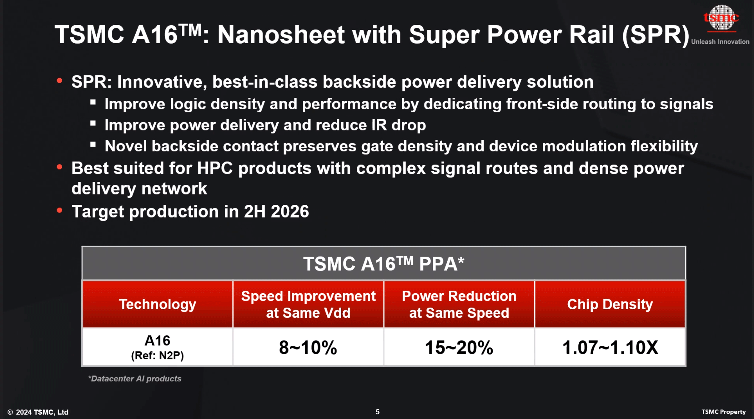
Headlining its Silicon Valley stop, TSMC announced its first 'angstrom-class' process technology: A16. Following a production schedule shift that has seen backside power delivery network technology (BSPDN) removed from TSMC's N2P node, the new 1.6nm-class production node will now be the first process to introduce BSPDN to TSMC's chipmaking repertoire. With the addition of backside power capabilities and other improvements, TSMC expects A16 to offer significantly improved performance and energy efficiency compared to TSMC's N2P fabrication process. It will be available to TSMC's clients starting H2 2026.
At a high level, TSMC's A16 process technology will rely on gate-all-around (GAAFET) nanosheet transistors and will feature a backside power rail, which will both improve power delivery and moderately increase transistor density. Compared to TSMC's N2P fabrication process, A16 is expected to offer a performance improvement of 8% to 10% at the same voltage and complexity, or a 15% to 20% reduction in power consumption at the same frequency and transistor count. TSMC is not listing detailed density parameters this far out, but the company says that chip density will increase by 1.07x to 1.10x – keeping in mind that transistor density heavily depends on the type and libraries of transistors used.
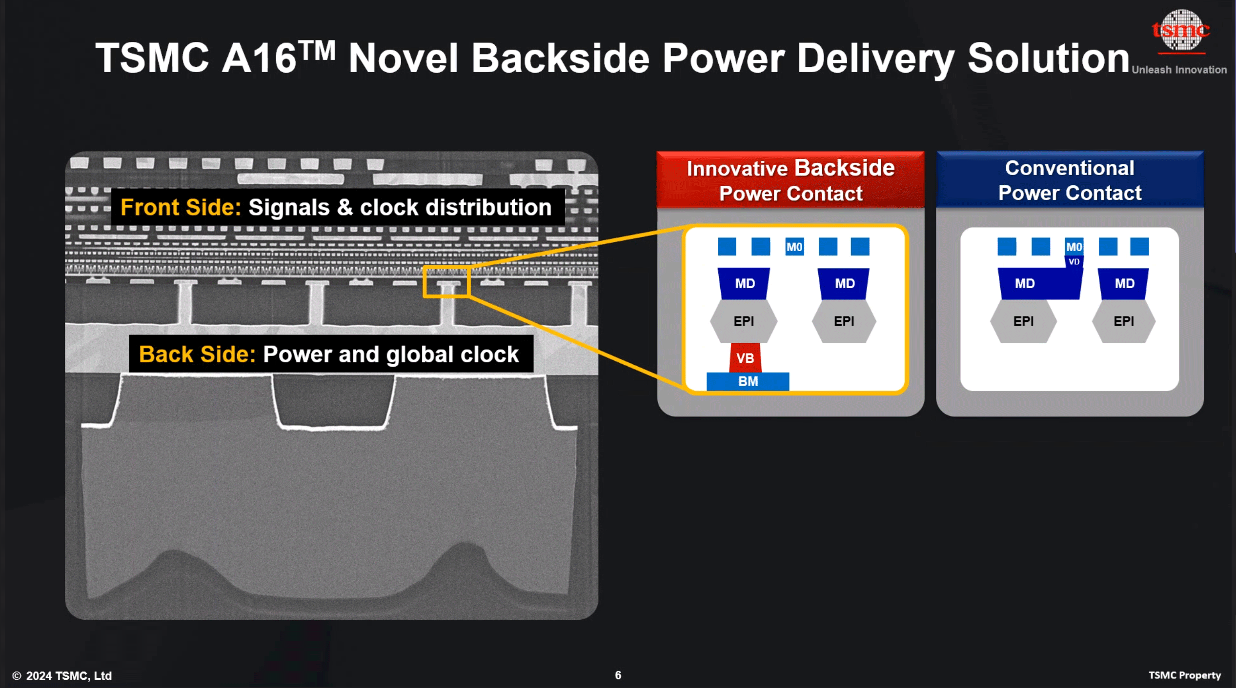
The key innovation of TSMC's A16 node, is its Super Power Rail (SPR) backside power delivery network, a first for TSMC. The contract chipmaker claims that A16's SPR is specifically tailored for high-performance computing products that feature both complex signal routes and dense power circuitry.
As noted earlier, with this week's announcement, A16 has now become the launch vehicle for backside power delivery at TSMC. The company was initially slated to offer BSPDN technology with N2P in 2026, but for reasons that aren't entirely clear, the tech has been punted from N2P and moved to A16. TSMC's official timing for N2P in 2023 was always a bit loose, so it's hard to say if this represents much of a practical delay for BSPDN at TSMC. But at the same time, it's important to underscore that A16 isn't just N2P renamed, but rather it will be a distinct technology from N2P.
TSMC is not the only fab pursuing backside power delivery, and accordingly, we're seeing multiple variations on the technique crop up at different fabs. The... Semiconductors

Standard CPU coolers, while adequate for managing basic thermal loads, often fall short in terms of noise reduction and superior cooling efficiency. This limitation drives advanced users and system builders to seek aftermarket solutions tailored to their specific needs. The high-end aftermarket cooler market is highly competitive, with manufacturers striving to offer products with exceptional performance.
Endorfy, previously known as SilentiumPC, is a Polish manufacturer that has undergone a significant transformation to expand its presence in global markets. The brand is known for delivering high-performance cooling solutions with a strong focus on balancing efficiency and affordability. By rebranding as Endorfy, the company aims to enter premium market segments while continuing to offer reliable, high-quality cooling products.
SilentiumPC became very popular in the value/mainstream segments of the PC market with their products, the spearhead of which probably was the Fera 5 cooler that we reviewed a little over two years ago and had a remarkable value for money. Today’s review places Endorfy’s largest CPU cooler, the Fortis 5 Dual Fan, on our laboratory test bench. The Fortis 5 is the largest CPU air cooler the company currently offers and is significantly more expensive than the Fera 5, yet it still is a single-tower cooler that strives to strike a balance between value, compatibility, and performance.
Cases/Cooling/PSUs![Micron: U.S. Fabs Will Start Operating in 2026 - 2029 <p align="center"><a href="https://www.anandtech.com/show/21459/micron-u-s-fabs-will-start-operating-in-2026-2029"><img src="https://images.anandtech.com/doci/21459/micron-server-datacenter-general-generic-678_575px.jpg" alt="" /></a></p><p><p>When Micron announced plans to build two new fabs in the U.S. in 2022, the company vaguely said both would come online by the decade's end. Then, in 2023, it began to optimize its spending, which pushed production at these fabrication facilities. This week, the company outlined more precise timeframes for when its fabs in <a href="https://www.anandtech.com/show/17573/micron-breaks-ground-on-its-15-billion-euv-dram-fab-in-the-us">Idaho</a> and <a href="https://www.anandtech.com/show/17606/micron-announces-100-billion-us-fab-complex-a-20year-plan">New York</a> will start operations: this will happen from calendar 2026 to calendar 2029.</p>
<p>"<em>These fab construction investments are necessary to support supply growth for the latter half of this decade,</em>" a statement by Micron in its Q3 FY2024 financial results report <a href="https://investors.micron.com/static-files/a531c7f0-fca2-48f3-8f24-79c945aaa2d2">reads</a>. "<em>This Idaho fab will not contribute to meaningful bit supply until fiscal 2027 and the New York construction capex is not expected to contribute to bit supply growth until fiscal 2028 or later. The timing of future [wafer fab equipment] spend in these fabs will be managed to align supply growth with expected demand growth.</em>"</p>
<p>Micron's fiscal year 2027 starts in September 2026, so the new fab near Boise, Idaho, is set to start operations between September 2026 and September 2027. The company's fiscal 2028 starts in September 2027, so the fab will likely begin operations in calendar 2028 or later, probably depending on the demand for DRAM memory in the coming years. That said, Micron's U.S. memory fabs will begin operations between late 2026 and 2029, which aligns with the company's original plans. </p>
<p>Construction of the fab in Idaho is well underway. In contrast, construction of the New York facility has yet to begin as the company is working on regulatory and permitting processes in the state. </p>
<p>Micron's capital expenditure (CaPex) plan for FY2024 is approximately $8.0 billion, with a decrease in year-over-year spending on wafer fabrication equipment (WFE). In Q4 FY2024, the company will spend around $3 billion on fab construction, new wafer fab tools, and various expansions/upgrades.</p>
<p>Looking ahead to FY2025, the company plans a substantial increase in capex, targeting a mid-30s percentage of revenue to support various technological and facility advancements. In particular, it expects its quarterly CapEx to average above the $3 billion level seen in the fourth quarter of FY2024, which means that it plans to spend about $12 billion in its fiscal 2025, which begins in late September.</p>
<p>Half or more of the total CapEx increase in FY2025 (i.e., over $2 billion) will be allocated to constructing new fabs in Idaho and New York. Meanwhile, the FY2025 CapEx will significantly rise to fund high-bandwidth memory (HBM) assembly and testing and the construction of fabrication and back-end facilities. This increase also includes investments in technology transitions to meet growing demand. </p>
<p>"<em>Fab construction in Idaho is underway, and we are working diligently to complete the regulatory and permitting processes in New York,</em>" said Sanjay Mehrotra, chief executive officer of Micron, at the company's conference call with investors and financial analysts (via <a href="https://seekingalpha.com/article/4701253-micron-technology-inc-mu-q3-2024-earnings-call-transcript?source=content_type%3Areact%7Csection%3ATranscripts%7Csection_asset%3ATranscripts%7Cfirst_level_url%3Asymbol%7Cbutton%3ATitle%7Clock_status%3ANo%7Cline%3A1">SeekingAlpha</a>). "<em>This additional leading-edge greenfield capacity, along with continued technology transition investments in our Asia facilities, is required to meet long-term demand in the second half of this decade and beyond. These investments support our objective to maintain our current bit share over time and to grow our memory bit supply in line with long-term industry bit demand.</em>"</p>
</p> Memory](https://lh3.googleusercontent.com/blogger_img_proxy/AEn0k_vv4vvfcosK2Mcd5eiTDjr3Hh294wLrMzrTWnY_xK4lnDPyXluWZsVkrQohd1uSPeYHfM1Dwz8ViQhQn6xdF_iUMfShhtUeZJyX20I9x0oMU-KMkhvR22QoeI71MYDtlf31PHDO6RkZxfwRKnehrLOT0uDdgOfP2BxpORhuMVhCtkc=w72-h72-p-k-no-nu)

When Micron announced plans to build two new fabs in the U.S. in 2022, the company vaguely said both would come online by the decade's end. Then, in 2023, it began to optimize its spending, which pushed production at these fabrication facilities. This week, the company outlined more precise timeframes for when its fabs in Idaho and New York will start operations: this will happen from calendar 2026 to calendar 2029.
"These fab construction investments are necessary to support supply growth for the latter half of this decade," a statement by Micron in its Q3 FY2024 financial results report reads. "This Idaho fab will not contribute to meaningful bit supply until fiscal 2027 and the New York construction capex is not expected to contribute to bit supply growth until fiscal 2028 or later. The timing of future [wafer fab equipment] spend in these fabs will be managed to align supply growth with expected demand growth."
Micron's fiscal year 2027 starts in September 2026, so the new fab near Boise, Idaho, is set to start operations between September 2026 and September 2027. The company's fiscal 2028 starts in September 2027, so the fab will likely begin operations in calendar 2028 or later, probably depending on the demand for DRAM memory in the coming years. That said, Micron's U.S. memory fabs will begin operations between late 2026 and 2029, which aligns with the company's original plans.
Construction of the fab in Idaho is well underway. In contrast, construction of the New York facility has yet to begin as the company is working on regulatory and permitting processes in the state.
Micron's capital expenditure (CaPex) plan for FY2024 is approximately $8.0 billion, with a decrease in year-over-year spending on wafer fabrication equipment (WFE). In Q4 FY2024, the company will spend around $3 billion on fab construction, new wafer fab tools, and various expansions/upgrades.
Looking ahead to FY2025, the company plans a substantial increase in capex, targeting a mid-30s percentage of revenue to support various technological and facility advancements. In particular, it expects its quarterly CapEx to average above the $3 billion level seen in the fourth quarter of FY2024, which means that it plans to spend about $12 billion in its fiscal 2025, which begins in late September.
Half or more of the total CapEx increase in FY2025 (i.e., over $2 billion) will be allocated to constructing new fabs in Idaho and New York. Meanwhile, the FY2025 CapEx will significantly rise to fund high-bandwidth memory (HBM) assembly and testing and the construction of fabrication and back-end facilities. This increase also includes investments in technology transitions to meet growing demand.
"Fab construction in Idaho is underway, and we are working diligently to complete the regulatory and permitting processes in New York," said Sanjay Mehrotra, chief executive officer of Micron, at the company's conference call with investors and financial analysts (via SeekingAlpha). "This additional leading-edge greenfield capacity, along with continued technology transition investments in our Asia facilities, is required to meet long-term demand in the second half of this decade and beyond. These investments support our objective to maintain our current bit share over time and to grow our memory bit supply in line with long-term industry bit demand."
Memory

Kioxia's booth at FMS 2024 was a busy one with multiple technology demonstrations keeping visitors occupied. A walk-through of the BiCS 8 manufacturing process was the first to grab my attention. Kioxia and Western Digital announced the sampling of BiCS 8 in March 2023. We had touched briefly upon its CMOS Bonded Array (CBA) scheme in our coverage of Kioxial's 2Tb QLC NAND device and coverage of Western Digital's 128 TB QLC enterprise SSD proof-of-concept demonstration. At Kioxia's booth, we got more insights.

Traditionally, fabrication of flash chips involved placement of the associate logic circuitry (CMOS process) around the periphery of the flash array. The process then moved on to putting the CMOS under the cell array, but the wafer development process was serialized with the CMOS logic getting fabricated first followed by the cell array on top. However, this has some challenges because the cell array requires a high-temperature processing step to ensure higher reliability that can be detrimental to the health of the CMOS logic. Thanks to recent advancements in wafer bonding techniques, the new CBA process allows the CMOS wafer and cell array wafer to be processed independently in parallel and then pieced together, as shown in the models above.

The BiCS 8 3D NAND incorporates 218 layers, compared to 112 layers in BiCS 5 and 162 layers in BiCS 6. The company decided to skip over BiCS 7 (or, rather, it was probably a short-lived generation meant as an internal test vehicle). The generation retains the four-plane charge trap structure of BiCS 6. In its TLC avatar, it is available as a 1 Tbit device. The QLC version is available in two capacities - 1 Tbit and 2 Tbit.
Kioxia also noted that while the number of layers (218) doesn't compare favorably with the latest layer counts from the competition, its lateral scaling / cell shrinkage has enabled it to be competitive in terms of bit density as well as operating speeds (3200 MT/s). For reference, the latest shipping NAND from Micron - the G9 - has 276 layers with a bit density in TLC mode of 21 Gbit/mm2, and operates at up to 3600 MT/s. However, its 232L NAND operates only up to 2400 MT/s and has a bit density of 14.6 Gbit/mm2.
It must be noted that the CBA hybrid bonding process has advantages over the current processes used by other vendors - including Micron's CMOS under array (CuA) and SK hynix's 4D PUC (periphery-under-chip) developed in the late 2010s. It is expected that other NAND vendors will also move eventually to some variant of the hybrid bonding scheme used by Kioxia.
Storage
Lorem Ipsum is simply dummy text of the printing and typesetting industry. Lorem Ipsum has been the industry's.


 removed from TSMC's N2P node, the new 1.6nm-class production node will now be the first process to introduce BSPDN to TSMC's chipmaking repertoire. With the addition of backside power capabilities and other improvements, TSMC expects A16 to offer significantly improved performance and energy efficiency compared to TSMC's N2P fabrication process. It will be available to TSMC's clients starting H2 2026.</p>
<h3>TSMC A16: Combining GAAFET With Backside Power Delivery</h3>
<p>At a high level, TSMC's A16 process technology will rely on gate-all-around (GAAFET) nanosheet transistors and will feature a backside power rail, which will both improve power delivery and moderately increase transistor density. Compared to TSMC's N2P fabrication process, A16 is expected to offer a performance improvement of 8% to 10% at the same voltage and complexity, or a 15% to 20% reduction in power consumption at the same frequency and transistor count. TSMC is not listing detailed density parameters this far out, but the company says that chip density will increase by 1.07x to 1.10x – keeping in mind that transistor density heavily depends on the type and libraries of transistors used.</p>
<p style="text-align: center;"><a href="https://www.anandtech.com/show/21369/tsmcs-16nm-technology-announced-for-late-2026-a16-with-super-power-rail-bspdn"><img alt="" src="https://images.anandtech.com/doci/21369/tsmc-a16-spr.png" style="width: 100%;" /></a></p>
<p>The key innovation of TSMC's A16 node, is its Super Power Rail (SPR) backside power delivery network, a first for TSMC. The contract chipmaker claims that A16's SPR is specifically tailored for high-performance computing products that feature both complex signal routes and dense power circuitry.</p>
<p>As noted earlier, with this week's announcement, A16 has now become the launch vehicle for backside power delivery at TSMC. The company was <a href="https://www.anandtech.com/show/18832/tsmc-outlines-2nm-plans-n2p-brings-backside-power-delivery-in-2026-n2x-added-to-roadmap">initially slated to offer BSPDN technology with N2P in 2026</a>, but for reasons that aren't entirely clear, the tech has been punted from N2P and moved to A16. TSMC's official timing for N2P in 2023 was always a bit loose, so it's hard to say if this represents much of a practical delay for BSPDN at TSMC. But at the same time, it's important to underscore that A16 isn't just N2P renamed, but rather it will be a distinct technology from N2P.</p>
<p style="text-align: center;"><a href="https://www.anandtech.com/show/21369/tsmcs-16nm-technology-announced-for-late-2026-a16-with-super-power-rail-bspdn"><img alt="" src="https://images.anandtech.com/doci/21369/tsmc-bspdn.png" style="width: 100%;" /></a></p>
<p>TSMC is not the only fab pursuing backside power delivery, and accordingly, we're seeing multiple variations on the technique crop up at different fabs. The... Semiconductors)
 removed from TSMC's N2P node, the new 1.6nm-class production node will now be the first process to introduce BSPDN to TSMC's chipmaking repertoire. With the addition of backside power capabilities and other improvements, TSMC expects A16 to offer significantly improved performance and energy efficiency compared to TSMC's N2P fabrication process. It will be available to TSMC's clients starting H2 2026.</p>
<h3>TSMC A16: Combining GAAFET With Backside Power Delivery</h3>
<p>At a high level, TSMC's A16 process technology will rely on gate-all-around (GAAFET) nanosheet transistors and will feature a backside power rail, which will both improve power delivery and moderately increase transistor density. Compared to TSMC's N2P fabrication process, A16 is expected to offer a performance improvement of 8% to 10% at the same voltage and complexity, or a 15% to 20% reduction in power consumption at the same frequency and transistor count. TSMC is not listing detailed density parameters this far out, but the company says that chip density will increase by 1.07x to 1.10x – keeping in mind that transistor density heavily depends on the type and libraries of transistors used.</p>
<p style="text-align: center;"><a href="https://www.anandtech.com/show/21369/tsmcs-16nm-technology-announced-for-late-2026-a16-with-super-power-rail-bspdn"><img alt="" src="https://images.anandtech.com/doci/21369/tsmc-a16-spr.png" style="width: 100%;" /></a></p>
<p>The key innovation of TSMC's A16 node, is its Super Power Rail (SPR) backside power delivery network, a first for TSMC. The contract chipmaker claims that A16's SPR is specifically tailored for high-performance computing products that feature both complex signal routes and dense power circuitry.</p>
<p>As noted earlier, with this week's announcement, A16 has now become the launch vehicle for backside power delivery at TSMC. The company was <a href="https://www.anandtech.com/show/18832/tsmc-outlines-2nm-plans-n2p-brings-backside-power-delivery-in-2026-n2x-added-to-roadmap">initially slated to offer BSPDN technology with N2P in 2026</a>, but for reasons that aren't entirely clear, the tech has been punted from N2P and moved to A16. TSMC's official timing for N2P in 2023 was always a bit loose, so it's hard to say if this represents much of a practical delay for BSPDN at TSMC. But at the same time, it's important to underscore that A16 isn't just N2P renamed, but rather it will be a distinct technology from N2P.</p>
<p style="text-align: center;"><a href="https://www.anandtech.com/show/21369/tsmcs-16nm-technology-announced-for-late-2026-a16-with-super-power-rail-bspdn"><img alt="" src="https://images.anandtech.com/doci/21369/tsmc-bspdn.png" style="width: 100%;" /></a></p>
<p>TSMC is not the only fab pursuing backside power delivery, and accordingly, we're seeing multiple variations on the technique crop up at different fabs. The... Semiconductors | https://compbuddey.blogspot.com/2024/04/tsmcs-16nm-technology-announced-for_28.html)
 removed from TSMC's N2P node, the new 1.6nm-class production node will now be the first process to introduce BSPDN to TSMC's chipmaking repertoire. With the addition of backside power capabilities and other improvements, TSMC expects A16 to offer significantly improved performance and energy efficiency compared to TSMC's N2P fabrication process. It will be available to TSMC's clients starting H2 2026.</p>
<h3>TSMC A16: Combining GAAFET With Backside Power Delivery</h3>
<p>At a high level, TSMC's A16 process technology will rely on gate-all-around (GAAFET) nanosheet transistors and will feature a backside power rail, which will both improve power delivery and moderately increase transistor density. Compared to TSMC's N2P fabrication process, A16 is expected to offer a performance improvement of 8% to 10% at the same voltage and complexity, or a 15% to 20% reduction in power consumption at the same frequency and transistor count. TSMC is not listing detailed density parameters this far out, but the company says that chip density will increase by 1.07x to 1.10x – keeping in mind that transistor density heavily depends on the type and libraries of transistors used.</p>
<p style="text-align: center;"><a href="https://www.anandtech.com/show/21369/tsmcs-16nm-technology-announced-for-late-2026-a16-with-super-power-rail-bspdn"><img alt="" src="https://images.anandtech.com/doci/21369/tsmc-a16-spr.png" style="width: 100%;" /></a></p>
<p>The key innovation of TSMC's A16 node, is its Super Power Rail (SPR) backside power delivery network, a first for TSMC. The contract chipmaker claims that A16's SPR is specifically tailored for high-performance computing products that feature both complex signal routes and dense power circuitry.</p>
<p>As noted earlier, with this week's announcement, A16 has now become the launch vehicle for backside power delivery at TSMC. The company was <a href="https://www.anandtech.com/show/18832/tsmc-outlines-2nm-plans-n2p-brings-backside-power-delivery-in-2026-n2x-added-to-roadmap">initially slated to offer BSPDN technology with N2P in 2026</a>, but for reasons that aren't entirely clear, the tech has been punted from N2P and moved to A16. TSMC's official timing for N2P in 2023 was always a bit loose, so it's hard to say if this represents much of a practical delay for BSPDN at TSMC. But at the same time, it's important to underscore that A16 isn't just N2P renamed, but rather it will be a distinct technology from N2P.</p>
<p style="text-align: center;"><a href="https://www.anandtech.com/show/21369/tsmcs-16nm-technology-announced-for-late-2026-a16-with-super-power-rail-bspdn"><img alt="" src="https://images.anandtech.com/doci/21369/tsmc-bspdn.png" style="width: 100%;" /></a></p>
<p>TSMC is not the only fab pursuing backside power delivery, and accordingly, we're seeing multiple variations on the technique crop up at different fabs. The... Semiconductors&body=https://compbuddey.blogspot.com/2024/04/tsmcs-16nm-technology-announced-for_28.html)
0 Comments