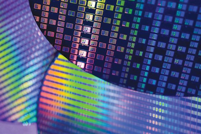

Taiwan Semiconductor Manufacturing Co. this week released its financial results for Q1 2024. Due to a rebound in demand for semiconductors, the company garned $18.87 billion in revenue for the quarter, which is up 12.9% year-over-year, but a decline of 3.8% quarter-over-quarter. The company says that in increase in demand for HPC processors (which includes processors for AI, PCs, and servers) drove its revenue rebound in Q1, but surprisingly, revenue share of TSMC's flagship N3 (3nm-class) process technology declined steeply quarter-over-quarter.
"Our business in the first quarter was impacted by smartphone seasonality, partially offset by continued HPC-related demand," said Wendell Huang, senior VP and chief financial officer of TSMC. "Moving into second quarter 2024, we expect our business to be supported by strong demand for our industry-leading 3nm and 5nm technologies, partially offset by continued smartphone seasonality."
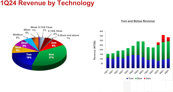
In the first quarter of 2024, N3 wafer sales accounted for 9% of the foundry's revenue, down from 15% in Q4 2023, and up from 6% in Q3 2023. In terms of dollars, TSMC's 3nm production brought in around $1.698 billion, which is lower than $2.943 billion in the previous quarter. Meanwhile, TSMC's other advanced process technologies increased their revenue share: N5 (5 nm-class) accounted for 37% (up from 35%), and N7 (7 nm-class) commanded 19% (up from 17%). Though both remained relatively flat in terms of revenue, at $6.981 billion and $3.585 billion, respectively.
Generally, advanced technology nodes (N7, N5, N3) generated 65% of TSMC's revenue (down 2% from Q4 2023), while the broader category of FinFET-based process technologies contributed 74% to the company's total wafer revenue (down 1% from the previous quarter).
TSMC itself attributes the steep decline of N3's contribution to seasonally lower demand for smartphones in the first quarter as compared to the fourth quarter, which may indeed be the case as demand for iPhones typically slowdowns in Q1. Along those lines, there have also been reports about a drop in demand for the latest iPhones in China.
But even if A17 Pro production volumes are down, Apple remains TSMC's lead customer for N3B, as the fab also produces their M3, M3 Pro, and M3 Max processors on the same node. These SoCs are larger in terms of die sizes and resulting costs, so their contribution to TSMC's revenue should be quite substantial.
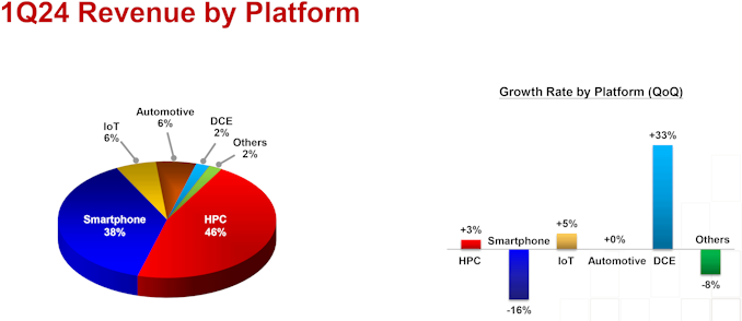
"Moving on to revenue contribution by platform. HPC increased 3% quarter-over-quarter to account for 46% of our first quarter revenue," said Huang. "Smartphone decreased 16% to account for 38%. IoT increased 5% to account for 6%. Automotive remained flat and accounted for 6%, and DCE increased 33% to account for 2%."
Meanwhile, as demand for AI and HPC processors will continue to increase in the coming years, TSMC expects its HPC platform to keep increasing its share in its revenue going forward.
"We expect several AI processors to be the strongest driver of our HPC platform growth and the largest contributor in terms of our overall incremental revenue growth in the next several years," said C.C. Wei, chief executive of TSMC.

Thanks to the success of the burgeoning market for AI accelerators, NVIDIA has been on a tear this year. And the only place that’s even more apparent than the company’s rapidly growing revenues is in the company’s stock price and market capitalization. After breaking into the top 5 most valuable companies only earlier this year, NVIDIA has reached the apex of Wall Street, closing out today as the world’s most valuable company.
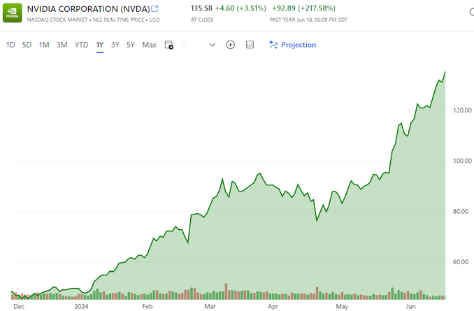
With a closing price of $135.58 on a day that saw NVIDIA’s stock pop up another 3.5%, NVIDIA has topped both Microsoft and Apple in valuation, reaching a market capitalization of $3.335 trillion. This follows a rapid rise in the company’s stock price, which has increased by 47% in the last month alone – particularly on the back of NVIDIA’s most recent estimates-beating earnings report – as well as a recent 10-for-1 stock split. And looking at the company’s performance over a longer time period, NVIDIA’s stock jumped a staggering 218% over the last year, or a mere 3,474% over the last 5 years.
NVIDIA’s ascension continues a trend over the last several years of tech companies all holding the top spots in the market capitalization rankings. Though this is the first time in quite a while that the traditional tech leaders of Apple and Microsoft have been pushed aside.
| Market Capitalization Rankings | ||
| Market Cap | Stock Price | |
| NVIDIA | $3.335T | $135.58 |
| Microsoft | $3.317T | $446.34 |
| Apple | $3.285T | $214.29 |
| Alphabet | $2.170T | $176.45 |
| Amazon | $1.902T | $182.81 |
Driving the rapid growth of NVIDIA and its market capitalization has been demand for AI accelerators from NVIDIA, particularly the company’s server-grade H100, H200, and GH200 accelerators for AI training. As the demand for these products has spiked, NVIDIA has been scaling up accordingly, repeatedly beating market expectations for how many of the accelerators they can ship – and what price they can charge. And despite all that growth, orders for NVIDIA’s high-end accelerators are still backlogged, underscoring how NVIDIA still isn’t meeting the full demands of hyperscalers and other enterprises.
Consequently, NVIDIA’s stock price and market capitalization have been on a tear on the basis of these future expectations. With a price-to-earnings (P/E) ratio of 76.7 – more than twice that of Microsoft or Apple – NVIDIA is priced more like a start-up than a 30-year-old tech company. But then it goes without saying that most 30-year-old tech companies aren’t tripling their revenue in a single year, placing NVIDIA in a rather unique situation at this time.
Like the stock market itself, market capitalizations are highly volatile. And historically speaking, it’s far from guaranteed that NVIDIA will be able to hold the top spot for long, never mind day-to-day fluctuations. NVIDIA, Apple, and Microsoft’s valuations are all within $50 billion (1.%) of each other, so for the moment at least, it’s still a tight race between all three companies. But no matter what happens from here, NVIDIA gets the exceptionally rare claim of having been the most valuable company in the world at some point.
(Carousel image courtesy MSN Money)
GPUs

Kioxia's booth at FMS 2024 was a busy one with multiple technology demonstrations keeping visitors occupied. A walk-through of the BiCS 8 manufacturing process was the first to grab my attention. Kioxia and Western Digital announced the sampling of BiCS 8 in March 2023. We had touched briefly upon its CMOS Bonded Array (CBA) scheme in our coverage of Kioxial's 2Tb QLC NAND device and coverage of Western Digital's 128 TB QLC enterprise SSD proof-of-concept demonstration. At Kioxia's booth, we got more insights.

Traditionally, fabrication of flash chips involved placement of the associate logic circuitry (CMOS process) around the periphery of the flash array. The process then moved on to putting the CMOS under the cell array, but the wafer development process was serialized with the CMOS logic getting fabricated first followed by the cell array on top. However, this has some challenges because the cell array requires a high-temperature processing step to ensure higher reliability that can be detrimental to the health of the CMOS logic. Thanks to recent advancements in wafer bonding techniques, the new CBA process allows the CMOS wafer and cell array wafer to be processed independently in parallel and then pieced together, as shown in the models above.

The BiCS 8 3D NAND incorporates 218 layers, compared to 112 layers in BiCS 5 and 162 layers in BiCS 6. The company decided to skip over BiCS 7 (or, rather, it was probably a short-lived generation meant as an internal test vehicle). The generation retains the four-plane charge trap structure of BiCS 6. In its TLC avatar, it is available as a 1 Tbit device. The QLC version is available in two capacities - 1 Tbit and 2 Tbit.
Kioxia also noted that while the number of layers (218) doesn't compare favorably with the latest layer counts from the competition, its lateral scaling / cell shrinkage has enabled it to be competitive in terms of bit density as well as operating speeds (3200 MT/s). For reference, the latest shipping NAND from Micron - the G9 - has 276 layers with a bit density in TLC mode of 21 Gbit/mm2, and operates at up to 3600 MT/s. However, its 232L NAND operates only up to 2400 MT/s and has a bit density of 14.6 Gbit/mm2.
It must be noted that the CBA hybrid bonding process has advantages over the current processes used by other vendors - including Micron's CMOS under array (CuA) and SK hynix's 4D PUC (periphery-under-chip) developed in the late 2010s. It is expected that other NAND vendors will also move eventually to some variant of the hybrid bonding scheme used by Kioxia.
Storage
Thanks to the success of the burgeoning market for AI accelerators, NVIDIA has been on a tear this year. And the only place that’s even more apparent than the company’s rapidly growing revenues is in the company’s stock price and market capitalization. After breaking into the top 5 most valuable companies only earlier this year, NVIDIA has reached the apex of Wall Street, closing out today as the world’s most valuable company.
With a closing price of $135.58 on a day that saw NVIDIA’s stock pop up another 3.5%, NVIDIA has topped both Microsoft and Apple in valuation, reaching a market capitalization of $3.335 trillion. This follows a rapid rise in the company’s stock price, which has increased by 47% in the last month alone – particularly on the back of NVIDIA’s most recent estimates-beating earnings report – as well as a recent 10-for-1 stock split. And looking at the company’s performance over a longer time period, NVIDIA’s stock jumped a staggering 218% over the last year, or a mere 3,474% over the last 5 years.
NVIDIA’s ascension continues a trend over the last several years of tech companies all holding the top spots in the market capitalization rankings. Though this is the first time in quite a while that the traditional tech leaders of Apple and Microsoft have been pushed aside.
| Market Capitalization Rankings | ||
| Market Cap | Stock Price | |
| NVIDIA | $3.335T | $135.58 |
| Microsoft | $3.317T | $446.34 |
| Apple | $3.285T | $214.29 |
| Alphabet | $2.170T | $176.45 |
| Amazon | $1.902T | $182.81 |
Driving the rapid growth of NVIDIA and its market capitalization has been demand for AI accelerators from NVIDIA, particularly the company’s server-grade H100, H200, and GH200 accelerators for AI training. As the demand for these products has spiked, NVIDIA has been scaling up accordingly, repeatedly beating market expectations for how many of the accelerators they can ship – and what price they can charge. And despite all that growth, orders for NVIDIA’s high-end accelerators are still backlogged, underscoring how NVIDIA still isn’t meeting the full demands of hyperscalers and other enterprises.
Consequently, NVIDIA’s stock price and market capitalization have been on a tear on the basis of these future expectations. With a price-to-earnings (P/E) ratio of 76.7 – more than twice that of Microsoft or Apple – NVIDIA is priced more like a start-up than a 30-year-old tech company. But then it goes without saying that most 30-year-old tech companies aren’t tripling their revenue in a single year, placing NVIDIA in a rather unique situation at this time.
Like the stock market itself, market capitalizations are highly volatile. And historically speaking, it’s far from guaranteed that NVIDIA will be able to hold the top spot for long, never mind day-to-day fluctuations. NVIDIA, Apple, and Microsoft’s valuations are all within $50 billion (1.%) of each other, so for the moment at least, it’s still a tight race between all three companies. But no matter what happens from here, NVIDIA gets the exceptionally rare claim of having been the most valuable company in the world at some point.
(Carousel image courtesy MSN Money)
GPUs
Kioxia's booth at FMS 2024 was a busy one with multiple technology demonstrations keeping visitors occupied. A walk-through of the BiCS 8 manufacturing process was the first to grab my attention. Kioxia and Western Digital announced the sampling of BiCS 8 in March 2023. We had touched briefly upon its CMOS Bonded Array (CBA) scheme in our coverage of Kioxial's 2Tb QLC NAND device and coverage of Western Digital's 128 TB QLC enterprise SSD proof-of-concept demonstration. At Kioxia's booth, we got more insights.
Traditionally, fabrication of flash chips involved placement of the associate logic circuitry (CMOS process) around the periphery of the flash array. The process then moved on to putting the CMOS under the cell array, but the wafer development process was serialized with the CMOS logic getting fabricated first followed by the cell array on top. However, this has some challenges because the cell array requires a high-temperature processing step to ensure higher reliability that can be detrimental to the health of the CMOS logic. Thanks to recent advancements in wafer bonding techniques, the new CBA process allows the CMOS wafer and cell array wafer to be processed independently in parallel and then pieced together, as shown in the models above.
The BiCS 8 3D NAND incorporates 218 layers, compared to 112 layers in BiCS 5 and 162 layers in BiCS 6. The company decided to skip over BiCS 7 (or, rather, it was probably a short-lived generation meant as an internal test vehicle). The generation retains the four-plane charge trap structure of BiCS 6. In its TLC avatar, it is available as a 1 Tbit device. The QLC version is available in two capacities - 1 Tbit and 2 Tbit.
Kioxia also noted that while the number of layers (218) doesn't compare favorably with the latest layer counts from the competition, its lateral scaling / cell shrinkage has enabled it to be competitive in terms of bit density as well as operating speeds (3200 MT/s). For reference, the latest shipping NAND from Micron - the G9 - has 276 layers with a bit density in TLC mode of 21 Gbit/mm2, and operates at up to 3600 MT/s. However, its 232L NAND operates only up to 2400 MT/s and has a bit density of 14.6 Gbit/mm2.
It must be noted that the CBA hybrid bonding process has advantages over the current processes used by other vendors - including Micron's CMOS under array (CuA) and SK hynix's 4D PUC (periphery-under-chip) developed in the late 2010s. It is expected that other NAND vendors will also move eventually to some variant of the hybrid bonding scheme used by Kioxia.
Storage

G.Skill on Tuesday introduced its ultra-low-latency DDR5-6400 memory modules that feature a CAS latency of 30 clocks, which appears to be the industry's most aggressive timings yet for DDR5-6400 sticks. The modules will be available for both AMD and Intel CPU-based systems.
With every new generation of DDR memory comes an increase in data transfer rates and an extension of relative latencies. While for the vast majority of applications, the increased bandwidth offsets the performance impact of higher timings, there are applications that favor low latencies. However, shrinking latencies is sometimes harder than increasing data transfer rates, which is why low-latency modules are rare.
Nonetheless, G.Skill has apparently managed to cherry-pick enough DDR5 memory chips and build appropriate printed circuit boards to produce DDR5-6400 modules with CL30 timings, which are substantially lower than the CL46 timings recommended by JEDEC for this speed bin. This means that while JEDEC-standard modules have an absolute latency of 14.375 ns, G.Skill's modules can boast a latency of just 9.375 ns – an approximately 35% decrease.
G.Skill's DDR5-6400 CL30 39-39-102 modules have a capacity of 16 GB and will be available in 32 GB dual-channel kits, though the company does not disclose voltages, which are likely considerably higher than those standardized by JEDEC.
The company plans to make its DDR5-6400 modules available both for AMD systems with EXPO profiles (Trident Z5 Neo RGB and Trident Z5 Royal Neo) and for Intel-powered PCs with XMP 3.0 profiles (Trident Z5 RGB and Trident Z5 Royal). For AMD AM5 systems that have a practical limitation of 6000 MT/s – 6400 MT/s for DDR5 memory (as this is roughly as fast as AMD's Infinity Fabric can operate at with a 1:1 ratio), the new modules will be particularly beneficial for AMD's Ryzen 7000 and Ryzen 9000-series processors.
G.Skill notes that since its modules are non-standard, they will not work with all systems but will operate on high-end motherboards with properly cooled CPUs.
The new ultra-low-latency memory kits will be available worldwide from G.Skill's partners starting in late August 2024. The company did not disclose the pricing of these modules, but since we are talking about premium products that boast unique specifications, they are likely to be priced accordingly.
Memory
Kioxia's booth at FMS 2024 was a busy one with multiple technology demonstrations keeping visitors occupied. A walk-through of the BiCS 8 manufacturing process was the first to grab my attention. Kioxia and Western Digital announced the sampling of BiCS 8 in March 2023. We had touched briefly upon its CMOS Bonded Array (CBA) scheme in our coverage of Kioxial's 2Tb QLC NAND device and coverage of Western Digital's 128 TB QLC enterprise SSD proof-of-concept demonstration. At Kioxia's booth, we got more insights.
Traditionally, fabrication of flash chips involved placement of the associate logic circuitry (CMOS process) around the periphery of the flash array. The process then moved on to putting the CMOS under the cell array, but the wafer development process was serialized with the CMOS logic getting fabricated first followed by the cell array on top. However, this has some challenges because the cell array requires a high-temperature processing step to ensure higher reliability that can be detrimental to the health of the CMOS logic. Thanks to recent advancements in wafer bonding techniques, the new CBA process allows the CMOS wafer and cell array wafer to be processed independently in parallel and then pieced together, as shown in the models above.
The BiCS 8 3D NAND incorporates 218 layers, compared to 112 layers in BiCS 5 and 162 layers in BiCS 6. The company decided to skip over BiCS 7 (or, rather, it was probably a short-lived generation meant as an internal test vehicle). The generation retains the four-plane charge trap structure of BiCS 6. In its TLC avatar, it is available as a 1 Tbit device. The QLC version is available in two capacities - 1 Tbit and 2 Tbit.
Kioxia also noted that while the number of layers (218) doesn't compare favorably with the latest layer counts from the competition, its lateral scaling / cell shrinkage has enabled it to be competitive in terms of bit density as well as operating speeds (3200 MT/s). For reference, the latest shipping NAND from Micron - the G9 - has 276 layers with a bit density in TLC mode of 21 Gbit/mm2, and operates at up to 3600 MT/s. However, its 232L NAND operates only up to 2400 MT/s and has a bit density of 14.6 Gbit/mm2.
It must be noted that the CBA hybrid bonding process has advantages over the current processes used by other vendors - including Micron's CMOS under array (CuA) and SK hynix's 4D PUC (periphery-under-chip) developed in the late 2010s. It is expected that other NAND vendors will also move eventually to some variant of the hybrid bonding scheme used by Kioxia.
Storage
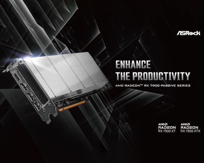
As sales of GPU-based AI accelerators remain as strong as ever, the immense demand for these cards has led to some server builders going off the beaten path in order to get the hardware they want at a lower price. While both NVIDIA and AMD offer official card configurations for servers, the correspondingly high price of these cards makes them a significant financial outlay that some customers either can't afford, or don't want to pay.
Instead, these groups have been turning to buying up consumer graphics cards, which although they come with additional limitations, are also a fraction of the cost of a "proper" server card. And this week, ASRock has removed another one of those limitations for would-be AMD Radeon users, with the introduction of a set of compact, passively-cooled Radeon RX 7900 XTX and RX 7900 XT video cards that are designed to go in servers.
Without any doubts, ASRock's AMD Radeon RX 7900 XTX Passive 24GB and AMD Radeon RX 7900 XT Passive 20GB AIBs are indeed graphics cards with four display outputs and based on the Navi 31 graphics processor (with 6144 and 5376 stream processors, respectively), so they can output graphics and work both with games and professional applications. And with TGPs of 355W and 315W respectively, these cards aren't underclocked in any way compared to traditional desktop cards. However, unlike a typical desktop card, the cooler on these cards is a dual-slot heatsink without any kind of fan attached, which is meant to be used with high-airflow forced-air cooling.
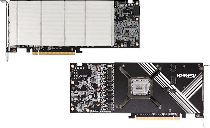
All-told, ASRock's passive cooler is pretty capable, as well; it's not just a simple aluminum heatsink. Beneath the fins, ASRock has gone with a vapor chamber and multiple heat pipes to distribute heat to the rest of the sink. Even with forced-air cooling in racked servers, the heatsink itself still needs to be efficient to keep a 300W+ card cool with only a dual-slot cooler – and especially so when upwards of four of these cards are installed side-by-side with each other. To make the boards even more server friendly, these cards are equipped with a 12V-2×6 power connector, a first for the Radeon RX 7900 series, simplifying installation by reducing cable clutter.
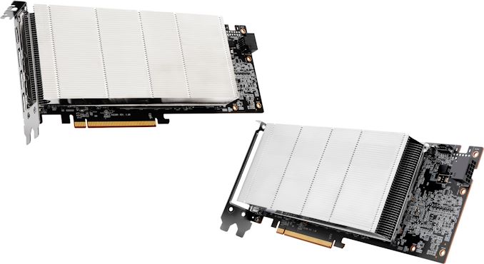
Driving the demand for these cards in particular is their memory configuration. With 24GB for the 7900 XTX and 20GB for the 7900 XT is half as much (or less) memory than can be found on AMD and NVIDIA's high-end professional and server cards, AMD is the only vendor offering consumer cards with this much memory for less than $1000. So for a memory-intensive AI inference cluster built on a low budget, the cheapest 24GB card available starts looking like a tantalizing option.
Otherwise, ASRock's Radeon RX 7900 Passive cards distinguish themselves from AMD's formal professional and server cards by what they're not capable of doing: namely, remote professional graphics or other applications that need things like GPU partitioning. These parts look to be aimed at one application only, artificial intelligence, and are meant to process huge amounts of data. For this purpose, their passive coolers will do the job and the lack of ProViz or VDI-oriented drives ensure that AMD will leave these lucrative markets for itself.
GPUs
The CXL consortium has had a regular presence at FMS (which rechristened itself from 'Flash Memory Summit' to the 'Future of Memory and Storage' this year). Back at FMS 2022, the company had announced v3.0 of the CXL specifications. This was followed by CXL 3.1's introduction at Supercomputing 2023. Having started off as a host to device interconnect standard, it had slowly subsumed other competing standards such as OpenCAPI and Gen-Z. As a result, the specifications started to encompass a wide variety of use-cases by building a protocol on top of the the ubiquitous PCIe expansion bus. The CXL consortium comprises of heavyweights such as AMD and Intel, as well as a large number of startup companies attempting to play in different segments on the device side. At FMS 2024, CXL had a prime position in the booth demos of many vendors.
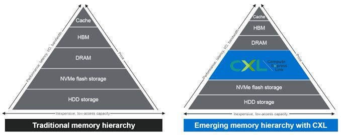
The migration of server platforms from DDR4 to DDR5, along with the rise of workloads demanding large RAM capacity (but not particularly sensitive to either memory bandwidth or latency), has opened up memory expansion modules as one of the first set of widely available CXL devices. Over the last couple of years, we have had product announcements from Samsung and Micron in this area.
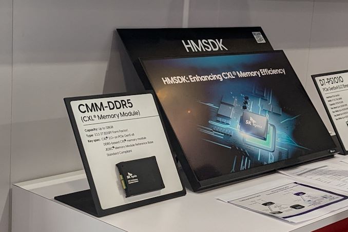
At FMS 2024, SK hynix was showing off their DDR5-based CMM-DDR5 CXL memory module with a 128 GB capacity. The company was also detailing their associated Heterogeneous Memory Software Development Kit (HMSDK) - a set of libraries and tools at both the kernel and user levels aimed at increasing the ease of use of CXL memory. This is achieved in part by considering the memory pyramid / hierarchy and relocating the data between the server's main memory (DRAM) and the CXL device based on usage frequency.
The CMM-DDR5 CXL memory module comes in the SDFF form-factor (E3.S 2T) with a PCIe 3.0 x8 host interface. The internal memory is based on 1α technology DRAM, and the device promises DDR5-class bandwidth and latency within a single NUMA hop. As these memory modules are meant to be used in datacenters and enterprises, the firmware includes features for RAS (reliability, availability, and serviceability) along with secure boot and other management features.
SK hynix was also demonstrating Niagara 2.0 - a hardware solution (currently based on FPGAs) to enable memory pooling and sharing - i.e, connecting multiple CXL memories to allow different hosts (CPUs and GPUs) to optimally share their capacity. The previous version only allowed capacity sharing, but the latest version enables sharing of data also. SK hynix had presented these solutions at the CXL DevCon 2024 earlier this year, but some progress seems to have been made in finalizing the specifications of the CMM-DDR5 at FMS 2024.
Micron had unveiled the CZ120 CXL Memory Expansion Module last year based on the Microchip SMC 2000 series CXL memory controller. At FMS 2024, Micron and Microchip had a demonstration of the module on a Granite Rapids server.
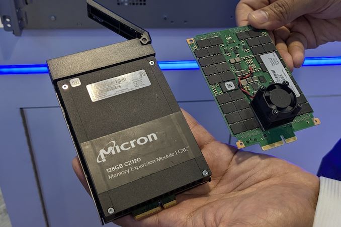
Additional insights into the SMC 2000 controller were also provided.
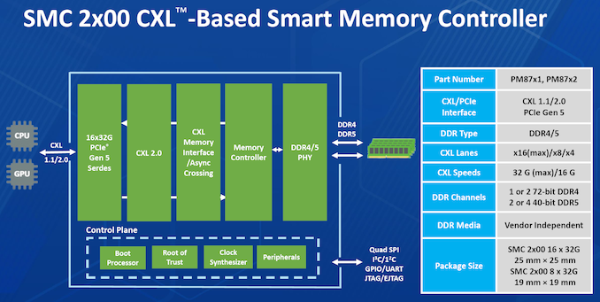
The CXL memory controller also incorporates DRAM die failure handling, and Microchip also provides diagnostics and debug tools to analyze failed modules. The memory controller also supports ECC, which forms part of the enterprise... Storage


Under the CHIPS & Science Act, the U.S. government provided tens of billions of dollars in grants and loans to the world's leading maker of chips, such as Intel, Samsung, and TSMC, which will significantly expand the country's semiconductor production industry in the coming years. However, most chips are typically tested, assembled, and packaged in Asia, which has left the American supply chain incomplete. Addressing this last gap in the government's domestic chip production plans, these past couple of weeks the U.S. government signed memorandums of understanding worth about $1.5 billion with Amkor and SK hynix to support their efforts to build chip packaging facilities in the U.S.
Amkor plans to build a $2 billion advanced packaging facility near Peoria, Arizona, to test and assemble chips produced by TSMC at its Fab 21 near Phoenix, Arizona. The company signed a MOU that offers $400 million in direct funding and access to $200 million in loans under the CHIPS & Science Act. In addition, the company plans to take advantage of a 25% investment tax credit on eligible capital expenditures.
Set to be strategically positioned near TSMC's upcoming Fab 21 complex in Arizona, Amkor's Peoria facility will occupy 55 acres and, when fully completed, will feature over 500,000 square feet (46,451 square meters) of cleanroom space, more than twice the size of Amkor's advanced packaging site in Vietnam. Although the company has not disclosed the exact capacity or the specific technologies the facility will support, it is expected to cater to a wide range of industries, including automotive, high-performance computing, and mobile technologies. This suggests the new plant will offer diverse packaging solutions, including traditional, 2.5D, and 3D technologies.
Amkor has collaborated extensively with Apple on the vision and initial setup of the Peoria facility, as Apple is slated to be the facility's first and largest customer, marking a significant commitment from the tech giant. This partnership highlights the importance of the new facility in reinforcing the U.S. semiconductor supply chain and positioning Amkor as a key partner for companies relying on TSMC's manufacturing capabilities. The project is expected to generate around 2,000 jobs and is scheduled to begin operations in 2027.
This week SK hynix also signed a preliminary agreement with the U.S. government to receive up to $450 million in direct funding and $500 million in loans to build an advanced memory packaging facility in West Lafayette, Indiana.
The proposed facility is scheduled to begin operations in 2028, which means that it will assemble HBM4 or HBM4E memory. Meanwhile, DRAM devices for high bandwidth memory (HBM) stacks will still be produced in South Korea. Nonetheless, packing finished HBM4/HBM4E in the U.S. and possibly integrating these memory modules with high-end processors is a big deal.
In addition to building its packaging plant, SK hynix plans to collaborate with Purdue University and other local research institutions to advance semiconductor technology and packaging innovations. This partnership is intended to bolster research and development in the region, positioning the facility as a hub for AI technology and skilled employment.
Semiconductors
Lorem Ipsum is simply dummy text of the printing and typesetting industry. Lorem Ipsum has been the industry's.
Thanks to the success of the burgeoning market for AI accelerators, NVIDIA has been on a tear this year. And the only place that’s even more apparent than the company’s rapidly growing revenues is in the company’s stock price and market capitalization. After breaking into the top 5 most valuable companies only earlier this year, NVIDIA has reached the apex of Wall Street, closing out today as the world’s most valuable company.
With a closing price of $135.58 on a day that saw NVIDIA’s stock pop up another 3.5%, NVIDIA has topped both Microsoft and Apple in valuation, reaching a market capitalization of $3.335 trillion. This follows a rapid rise in the company’s stock price, which has increased by 47% in the last month alone – particularly on the back of NVIDIA’s most recent estimates-beating earnings report – as well as a recent 10-for-1 stock split. And looking at the company’s performance over a longer time period, NVIDIA’s stock jumped a staggering 218% over the last year, or a mere 3,474% over the last 5 years.
NVIDIA’s ascension continues a trend over the last several years of tech companies all holding the top spots in the market capitalization rankings. Though this is the first time in quite a while that the traditional tech leaders of Apple and Microsoft have been pushed aside.
| Market Capitalization Rankings | ||
| Market Cap | Stock Price | |
| NVIDIA | $3.335T | $135.58 |
| Microsoft | $3.317T | $446.34 |
| Apple | $3.285T | $214.29 |
| Alphabet | $2.170T | $176.45 |
| Amazon | $1.902T | $182.81 |
Driving the rapid growth of NVIDIA and its market capitalization has been demand for AI accelerators from NVIDIA, particularly the company’s server-grade H100, H200, and GH200 accelerators for AI training. As the demand for these products has spiked, NVIDIA has been scaling up accordingly, repeatedly beating market expectations for how many of the accelerators they can ship – and what price they can charge. And despite all that growth, orders for NVIDIA’s high-end accelerators are still backlogged, underscoring how NVIDIA still isn’t meeting the full demands of hyperscalers and other enterprises.
Consequently, NVIDIA’s stock price and market capitalization have been on a tear on the basis of these future expectations. With a price-to-earnings (P/E) ratio of 76.7 – more than twice that of Microsoft or Apple – NVIDIA is priced more like a start-up than a 30-year-old tech company. But then it goes without saying that most 30-year-old tech companies aren’t tripling their revenue in a single year, placing NVIDIA in a rather unique situation at this time.
Like the stock market itself, market capitalizations are highly volatile. And historically speaking, it’s far from guaranteed that NVIDIA will be able to hold the top spot for long, never mind day-to-day fluctuations. NVIDIA, Apple, and Microsoft’s valuations are all within $50 billion (1.%) of each other, so for the moment at least, it’s still a tight race between all three companies. But no matter what happens from here, NVIDIA gets the exceptionally rare claim of having been the most valuable company in the world at some point.
(Carousel image courtesy MSN Money)
GPUs


 drove its revenue rebound in Q1, but surprisingly, revenue share of TSMC's flagship N3 (3nm-class) process technology declined steeply quarter-over-quarter.</p>
<p>"Our business in the first quarter was impacted by smartphone seasonality, partially offset by continued HPC-related demand," said Wendell Huang, senior VP and chief financial officer of TSMC. "Moving into second quarter 2024, we expect our business to be supported by strong demand for our industry-leading 3nm and 5nm technologies, partially offset by continued smartphone seasonality."</p>
<p>In the first quarter of 2024, N3 wafer sales accounted for 9% of the foundry's revenue, down from 15% in Q4 2023, and up from 6% in Q3 2023. In terms of dollars, TSMC's 3nm production brought in around $1.698 billion, which is lower than $2.943 billion in the previous quarter. Meanwhile, TSMC's other advanced process technologies increased their revenue share: N5 (5 nm-class) accounted for 37% (up from 35%), and N7 (7 nm-class) commanded 19% (up from 17%). Though both remained relatively flat in terms of revenue, at $6.981 billion and $3.585 billion, respectively.</p>
<p>Generally, advanced technology nodes (N7, N5, N3) generated 65% of TSMC's revenue (down 2% from Q4 2023), while the broader category of FinFET-based process technologies contributed 74% to the company's total wafer revenue (down 1% from the previous quarter).</p>
<p style="text-align: center;"><a href="https://www.anandtech.com/show/21359/tsmc-posts-q124-results-3nm-revenue-share-drops-steeply-but-hpc-share-rises"><img alt="" src="https://images.anandtech.com/doci/21359/tsmc-q1-2024-nodes-revenue_575px.png" /></a></p>
<p>TSMC itself attributes the steep decline of N3's contribution to seasonally lower demand for smartphones in the first quarter as compared to the fourth quarter, which may indeed be the case as demand for iPhones typically slowdowns in Q1. Along those lines, there have also been reports about a drop in demand for the latest iPhones in China.</p>
<p>But even if A17 Pro production volumes are down, Apple remains TSMC's lead customer for N3B, as the fab also produces their M3, M3 Pro, and M3 Max processors on the same node. These SoCs are larger in terms of die sizes and resulting costs, so their contribution to TSMC's revenue should be quite substantial.</p>
<p style="text-align: center;"><a href="https://www.anandtech.com/show/21359/tsmc-posts-q124-results-3nm-revenue-share-drops-steeply-but-hpc-share-rises"><img alt="" src="https://images.anandtech.com/doci/21359/tsmc-q1-2024-platform-revenue_575px.png" /></a></p>
<p>"Moving on to revenue contribution by platform. HPC increased 3% quarter-over-quarter to account for 46% of our first quarter revenue," said Huang. "Smartphone decreased 16% to account for 38%. IoT increased 5% to account for 6%. Automotive remained flat and accounted for 6%, and DCE increased 33% to account for 2%."</p>
<p>Meanwhile, as demand for AI and HPC processors will continue to increase in the coming years, TSMC expects its HPC platform to keep increasing its share in its revenue going forward.<br />
<br />
"We expect several AI processors to be the strongest driver of our HPC platform growth and the largest contributor in terms of our overall incremental revenue growth in the next several years," said C.C. Wei, chief executive of TSMC.</p>
</p> Semiconductors)
 drove its revenue rebound in Q1, but surprisingly, revenue share of TSMC's flagship N3 (3nm-class) process technology declined steeply quarter-over-quarter.</p>
<p>"Our business in the first quarter was impacted by smartphone seasonality, partially offset by continued HPC-related demand," said Wendell Huang, senior VP and chief financial officer of TSMC. "Moving into second quarter 2024, we expect our business to be supported by strong demand for our industry-leading 3nm and 5nm technologies, partially offset by continued smartphone seasonality."</p>
<p>In the first quarter of 2024, N3 wafer sales accounted for 9% of the foundry's revenue, down from 15% in Q4 2023, and up from 6% in Q3 2023. In terms of dollars, TSMC's 3nm production brought in around $1.698 billion, which is lower than $2.943 billion in the previous quarter. Meanwhile, TSMC's other advanced process technologies increased their revenue share: N5 (5 nm-class) accounted for 37% (up from 35%), and N7 (7 nm-class) commanded 19% (up from 17%). Though both remained relatively flat in terms of revenue, at $6.981 billion and $3.585 billion, respectively.</p>
<p>Generally, advanced technology nodes (N7, N5, N3) generated 65% of TSMC's revenue (down 2% from Q4 2023), while the broader category of FinFET-based process technologies contributed 74% to the company's total wafer revenue (down 1% from the previous quarter).</p>
<p style="text-align: center;"><a href="https://www.anandtech.com/show/21359/tsmc-posts-q124-results-3nm-revenue-share-drops-steeply-but-hpc-share-rises"><img alt="" src="https://images.anandtech.com/doci/21359/tsmc-q1-2024-nodes-revenue_575px.png" /></a></p>
<p>TSMC itself attributes the steep decline of N3's contribution to seasonally lower demand for smartphones in the first quarter as compared to the fourth quarter, which may indeed be the case as demand for iPhones typically slowdowns in Q1. Along those lines, there have also been reports about a drop in demand for the latest iPhones in China.</p>
<p>But even if A17 Pro production volumes are down, Apple remains TSMC's lead customer for N3B, as the fab also produces their M3, M3 Pro, and M3 Max processors on the same node. These SoCs are larger in terms of die sizes and resulting costs, so their contribution to TSMC's revenue should be quite substantial.</p>
<p style="text-align: center;"><a href="https://www.anandtech.com/show/21359/tsmc-posts-q124-results-3nm-revenue-share-drops-steeply-but-hpc-share-rises"><img alt="" src="https://images.anandtech.com/doci/21359/tsmc-q1-2024-platform-revenue_575px.png" /></a></p>
<p>"Moving on to revenue contribution by platform. HPC increased 3% quarter-over-quarter to account for 46% of our first quarter revenue," said Huang. "Smartphone decreased 16% to account for 38%. IoT increased 5% to account for 6%. Automotive remained flat and accounted for 6%, and DCE increased 33% to account for 2%."</p>
<p>Meanwhile, as demand for AI and HPC processors will continue to increase in the coming years, TSMC expects its HPC platform to keep increasing its share in its revenue going forward.<br />
<br />
"We expect several AI processors to be the strongest driver of our HPC platform growth and the largest contributor in terms of our overall incremental revenue growth in the next several years," said C.C. Wei, chief executive of TSMC.</p>
</p> Semiconductors | https://compbuddey.blogspot.com/2024/04/tsmc-posts-q124-results-3nm-revenue_20.html)
 drove its revenue rebound in Q1, but surprisingly, revenue share of TSMC's flagship N3 (3nm-class) process technology declined steeply quarter-over-quarter.</p>
<p>"Our business in the first quarter was impacted by smartphone seasonality, partially offset by continued HPC-related demand," said Wendell Huang, senior VP and chief financial officer of TSMC. "Moving into second quarter 2024, we expect our business to be supported by strong demand for our industry-leading 3nm and 5nm technologies, partially offset by continued smartphone seasonality."</p>
<p>In the first quarter of 2024, N3 wafer sales accounted for 9% of the foundry's revenue, down from 15% in Q4 2023, and up from 6% in Q3 2023. In terms of dollars, TSMC's 3nm production brought in around $1.698 billion, which is lower than $2.943 billion in the previous quarter. Meanwhile, TSMC's other advanced process technologies increased their revenue share: N5 (5 nm-class) accounted for 37% (up from 35%), and N7 (7 nm-class) commanded 19% (up from 17%). Though both remained relatively flat in terms of revenue, at $6.981 billion and $3.585 billion, respectively.</p>
<p>Generally, advanced technology nodes (N7, N5, N3) generated 65% of TSMC's revenue (down 2% from Q4 2023), while the broader category of FinFET-based process technologies contributed 74% to the company's total wafer revenue (down 1% from the previous quarter).</p>
<p style="text-align: center;"><a href="https://www.anandtech.com/show/21359/tsmc-posts-q124-results-3nm-revenue-share-drops-steeply-but-hpc-share-rises"><img alt="" src="https://images.anandtech.com/doci/21359/tsmc-q1-2024-nodes-revenue_575px.png" /></a></p>
<p>TSMC itself attributes the steep decline of N3's contribution to seasonally lower demand for smartphones in the first quarter as compared to the fourth quarter, which may indeed be the case as demand for iPhones typically slowdowns in Q1. Along those lines, there have also been reports about a drop in demand for the latest iPhones in China.</p>
<p>But even if A17 Pro production volumes are down, Apple remains TSMC's lead customer for N3B, as the fab also produces their M3, M3 Pro, and M3 Max processors on the same node. These SoCs are larger in terms of die sizes and resulting costs, so their contribution to TSMC's revenue should be quite substantial.</p>
<p style="text-align: center;"><a href="https://www.anandtech.com/show/21359/tsmc-posts-q124-results-3nm-revenue-share-drops-steeply-but-hpc-share-rises"><img alt="" src="https://images.anandtech.com/doci/21359/tsmc-q1-2024-platform-revenue_575px.png" /></a></p>
<p>"Moving on to revenue contribution by platform. HPC increased 3% quarter-over-quarter to account for 46% of our first quarter revenue," said Huang. "Smartphone decreased 16% to account for 38%. IoT increased 5% to account for 6%. Automotive remained flat and accounted for 6%, and DCE increased 33% to account for 2%."</p>
<p>Meanwhile, as demand for AI and HPC processors will continue to increase in the coming years, TSMC expects its HPC platform to keep increasing its share in its revenue going forward.<br />
<br />
"We expect several AI processors to be the strongest driver of our HPC platform growth and the largest contributor in terms of our overall incremental revenue growth in the next several years," said C.C. Wei, chief executive of TSMC.</p>
</p> Semiconductors&body=https://compbuddey.blogspot.com/2024/04/tsmc-posts-q124-results-3nm-revenue_20.html)
0 Comments