Hot Posts
Silicon Motion Demonstrates Flexible Data Placement on MonTitan Gen 5 Enterprise SSD Platform
At FMS 2024, the technological requirements from the storage and memory subsystem took center stage. Both SSD and controller vendors had various demonstrations touting their suitability for different stages of the AI data pipeline - ingestion, preparation, training, checkpointing, and inference. Vendors like Solidigm have different types of SSDs optimized for different stages of the pipeline. At the same time, controller vendors have taken advantage of one of the features introduced recently in the NVM Express standard - Flexible Data Placement (FDP).
FDP involves the host providing information / hints about the areas where the controller could place the incoming write data in order to reduce the write amplification. These hints are generated based on specific block sizes advertised by the device. The feature is completely backwards-compatible, with non-FDP hosts working just as before with FDP-enabled SSDs, and vice-versa.
Silicon Motion's MonTitan Gen 5 Enterprise SSD Platform was announced back in 2022. Since then, Silicon Motion has been touting the flexibility of the platform, allowing its customers to incorporate their own features as part of the customization process. This approach is common in the enterprise space, as we have seen with Marvell's Bravera SC5 SSD controller in the DapuStor SSDs and Microchip's Flashtec controllers in the Longsys FORESEE enterprise SSDs.
At FMS 2024, the company was demonstrating the advantages of flexible data placement by allowing a single QLC SSD based on their MonTitan platform to take part in different stages of the AI data pipeline while maintaining the required quality of service (minimum bandwidth) for each process. The company even has a trademarked name (PerformaShape) for the firmware feature in the controller that allows the isolation of different concurrent SSD accesses (from different stages in the AI data pipeline) to guarantee this QoS. Silicon Motion claims that this scheme will enable its customers to get the maximum write performance possible from QLC SSDs without negatively impacting the performance of other types of accesses.
Silicon Motion and Phison have market leadership in the client SSD controller market with similar approaches. However, their enterprise SSD controller marketing couldn't be more different. While Phison has gone in for a turnkey solution with their Gen 5 SSD platform (to the extent of not adopting the white label route for this generation, and instead opting to get the SSDs qualified with different cloud service providers themselves), Silicon Motion is opting for a different approach. The flexibility and customization possibilities can make platforms like the MonTitan appeal to flash array vendors.
StoragePopular Post
MediaTek to Add NVIDIA G-Sync Support to Monitor Scalers, Make G-Sync Displays More Accessible
NVIDIA on Tuesday said that future monitor scalers from MediaTek will support its G-Sync technologies. NVIDIA is partnering with MediaTek to integrate its full range of G-Sync technologies into future monitors without requiring a standalone G-Sync module, which makes advanced gaming features more accessible across a broader range of displays.
Traditionally, G-Sync technology relied on a dedicated G-sync module – based on an Altera FPGA – to handle syncing display refresh rates with the GPU in order to reduce screen tearing, stutter, and input lag. As a more basic solution, in 2019 NVIDIA introduced G-Sync Compatible certification and branding, which leveraged the industry-standard VESA AdaptiveSync technology to handle variable refresh rates. In lieu of using a dedicated module, leveraging AdaptiveSync allowed for cheaper monitors, with NVIDIA's program serving as a stamp of approval that the monitor worked with NVIDIA GPUs and met NVIDIA's performance requirements. Still, G-Sync Compatible monitors still lack some features that, to date, require the dedicated G-Sync module.
Through this new partnership with MediaTek, MediaTek will bring support for all of NVIDIA's G-Sync technologies, including the latest G-Sync Pulsar, directly into their scalers. G-Sync Pulsar enhances motion clarity and reduces ghosting, providing a smoother gaming experience. In addition to variable refresh rates and Pulsar, MediaTek-based G-Sync displays will support such features as variable overdrive, 12-bit color, Ultra Low Motion Blur, low latency HDR, and Reflex Analyzer. This integration will allow more monitors to support a full range of G-Sync features without having to incorporate an expensive FPGA.
The first monitors to feature full G-Sync support without needing an NVIDIA module include the AOC Agon Pro AG276QSG2, Acer Predator XB273U F5, and ASUS ROG Swift 360Hz PG27AQNR. These monitors offer 360Hz refresh rates, 1440p resolution, and HDR support.
What remains to be seen is which specific MediaTek's scalers will support NVIDIA's G-Sync technology – or if the company is going to implement support into all of their scalers going forward. It also remains to be seen whether monitors with NVIDIA's dedicated G-Sync modules retain any advantages over displays with MediaTek's scalers.
MonitorsRapidus Wants to Offer Fully Automated Packaging for 2nm Fab to Cut Chip Lead Times
One of the core challenges that Rapidus will face when it kicks off volume production of chips on its 2nm-class process technology in 2027 is lining up customers. With Intel, Samsung, and TSMC all slated to offer their own 2nm-class nodes by that time, Rapidus will need some kind of advantage to attract customers away from its more established rivals. To that end, the company thinks they've found their edge: fully automated packaging that will allow for shorter chip lead times than manned packaging operations.
In an interview with Nikkei, Rapidus' president, Atsuyoshi Koike, outlined the company's vision to use advanced packaging as a competitive edge for the new fab. The Hokkaido facility, which is currently under construction and is expecting to begin equipment installation this December, is already slated to both produce chips and offer advanced packaging services within the same facility, an industry first. But ultimately, Rapidus biggest plan to differentiate itself is by automating the back-end fab processes (chip packaging) to provide significantly faster turnaround times.
Rapidus is targetting back-end production in particular as, compared to front-end (lithography) production, back-end production still heavily relies on human labor. No other advanced packaging fab has fully automated the process thus far, which provides for a degree of flexibility, but slows throughput. But with automation in place to handle this aspect of chip production, Rapidus would be able to increase chip packaging efficiency and speed, which is crucial as chip assembly tasks become more complex. Rapidus is also collaborating with multiple Japanese suppliers to source materials for back-end production.
"In the past, Japanese chipmakers tried to keep their technology development exclusively in-house, which pushed up development costs and made them less competitive," Koike told Nikkei. "[Rapidus plans to] open up technology that should be standardized, bringing down costs, while handling important technology in-house."
Financially, Rapidus faces a significant challenge, needing a total of ¥5 trillion ($35 billion) by the time mass production starts in 2027. The company estimates that ¥2 trillion will be required by 2025 for prototype production. While the Japanese government has provided ¥920 billion in aid, Rapidus still needs to secure substantial funding from private investors.
Due to its lack of track record and experience of chip production as. well as limited visibility for success, Rapidus is finding it difficult to attract private financing. The company is in discussions with the government to make it easier to raise capital, including potential loan guarantees, and is hopeful that new legislation will assist in this effort.
SemiconductorsSearch This Blog
OfferNest
Subscribe Us
Most Popular
MediaTek to Add NVIDIA G-Sync Support to Monitor Scalers, Make G-Sync Displays More Accessible
NVIDIA on Tuesday said that future monitor scalers from MediaTek will support its G-Sync technologies. NVIDIA is partnering with MediaTek to integrate its full range of G-Sync technologies into future monitors without requiring a standalone G-Sync module, which makes advanced gaming features more accessible across a broader range of displays.
Traditionally, G-Sync technology relied on a dedicated G-sync module – based on an Altera FPGA – to handle syncing display refresh rates with the GPU in order to reduce screen tearing, stutter, and input lag. As a more basic solution, in 2019 NVIDIA introduced G-Sync Compatible certification and branding, which leveraged the industry-standard VESA AdaptiveSync technology to handle variable refresh rates. In lieu of using a dedicated module, leveraging AdaptiveSync allowed for cheaper monitors, with NVIDIA's program serving as a stamp of approval that the monitor worked with NVIDIA GPUs and met NVIDIA's performance requirements. Still, G-Sync Compatible monitors still lack some features that, to date, require the dedicated G-Sync module.
Through this new partnership with MediaTek, MediaTek will bring support for all of NVIDIA's G-Sync technologies, including the latest G-Sync Pulsar, directly into their scalers. G-Sync Pulsar enhances motion clarity and reduces ghosting, providing a smoother gaming experience. In addition to variable refresh rates and Pulsar, MediaTek-based G-Sync displays will support such features as variable overdrive, 12-bit color, Ultra Low Motion Blur, low latency HDR, and Reflex Analyzer. This integration will allow more monitors to support a full range of G-Sync features without having to incorporate an expensive FPGA.
The first monitors to feature full G-Sync support without needing an NVIDIA module include the AOC Agon Pro AG276QSG2, Acer Predator XB273U F5, and ASUS ROG Swift 360Hz PG27AQNR. These monitors offer 360Hz refresh rates, 1440p resolution, and HDR support.
What remains to be seen is which specific MediaTek's scalers will support NVIDIA's G-Sync technology – or if the company is going to implement support into all of their scalers going forward. It also remains to be seen whether monitors with NVIDIA's dedicated G-Sync modules retain any advantages over displays with MediaTek's scalers.
MonitorsRapidus Wants to Offer Fully Automated Packaging for 2nm Fab to Cut Chip Lead Times
One of the core challenges that Rapidus will face when it kicks off volume production of chips on its 2nm-class process technology in 2027 is lining up customers. With Intel, Samsung, and TSMC all slated to offer their own 2nm-class nodes by that time, Rapidus will need some kind of advantage to attract customers away from its more established rivals. To that end, the company thinks they've found their edge: fully automated packaging that will allow for shorter chip lead times than manned packaging operations.
In an interview with Nikkei, Rapidus' president, Atsuyoshi Koike, outlined the company's vision to use advanced packaging as a competitive edge for the new fab. The Hokkaido facility, which is currently under construction and is expecting to begin equipment installation this December, is already slated to both produce chips and offer advanced packaging services within the same facility, an industry first. But ultimately, Rapidus biggest plan to differentiate itself is by automating the back-end fab processes (chip packaging) to provide significantly faster turnaround times.
Rapidus is targetting back-end production in particular as, compared to front-end (lithography) production, back-end production still heavily relies on human labor. No other advanced packaging fab has fully automated the process thus far, which provides for a degree of flexibility, but slows throughput. But with automation in place to handle this aspect of chip production, Rapidus would be able to increase chip packaging efficiency and speed, which is crucial as chip assembly tasks become more complex. Rapidus is also collaborating with multiple Japanese suppliers to source materials for back-end production.
"In the past, Japanese chipmakers tried to keep their technology development exclusively in-house, which pushed up development costs and made them less competitive," Koike told Nikkei. "[Rapidus plans to] open up technology that should be standardized, bringing down costs, while handling important technology in-house."
Financially, Rapidus faces a significant challenge, needing a total of ¥5 trillion ($35 billion) by the time mass production starts in 2027. The company estimates that ¥2 trillion will be required by 2025 for prototype production. While the Japanese government has provided ¥920 billion in aid, Rapidus still needs to secure substantial funding from private investors.
Due to its lack of track record and experience of chip production as. well as limited visibility for success, Rapidus is finding it difficult to attract private financing. The company is in discussions with the government to make it easier to raise capital, including potential loan guarantees, and is hopeful that new legislation will assist in this effort.
SemiconductorsIntel Sells Its Arm Shares, Reduces Stakes in Other Companies
Intel has divested its entire stake in Arm Holdings during the second quarter, raising approximately $147 million. Alongside this, Intel sold its stake in cybersecurity firm ZeroFox and reduced its holdings in Astera Labs, all as part of a broader effort to manage costs and recover cash amid significant financial challenges.
The sale of Intel's 1.18 million shares in Arm Holdings, as reported in a recent SEC filing, comes at a time when the company is struggling with substantial financial losses. Despite the $147 million generated from the sale, Intel reported a $120 million net loss on its equity investments for the quarter, which is a part of a larger $1.6 billion loss that Intel faced during this period.
In addition to selling its stake in Arm, Intel also exited its investment in ZeroFox and reduced its involvement with Astera Labs, a company known for developing connectivity platforms for enterprise hardware. These moves are in line with Intel's strategy to reduce costs and stabilize its financial position as it faces ongoing market challenges.
Despite the divestment, Intel's past investment in Arm was likely driven by strategic considerations. Arm Holdings is a significant force in the semiconductor industry, with its designs powering most mobile devices, and, for obvious reasons, Intel would like to address these. Intel and Arm are also collaborating on datacenter platforms tailored for Intel's 18A process technology. Additionally, Arm might view Intel as a potential licensee for its technologies and a valuable partner for other companies that license Arm's designs.
Intel's investment in Astera Labs was also a strategic one as the company probably wanted to secure steady supply of smart retimers, smart cable modems, and CXL memory controller, which are used in volumes in datacenters and Intel is certainly interested in selling as many datacenter CPUs as possible.
Intel's financial struggles were highlighted earlier this month when the company released a disappointing earnings report, which led to a 33% drop in its stock value, erasing billions of dollars of capitalization. To counter these difficulties, Intel announced plans to cut 15,000 jobs and implement other expense reductions. The company has also suspended its dividend, signaling the depth of its efforts to conserve cash and focus on recovery. When it comes to divestment of Arm stock, the need for immediate financial stabilization has presumably taken precedence, leading to the decision.
CPUsKioxia Demonstrates Optical Interface SSDs for Data Centers
A few years back, the Japanese government's New Energy and Industrial Technology Development Organization (NEDO ) allocated funding for the development of green datacenter technologies. With the aim to obtain up to 40% savings in overall power consumption, several Japanese companies have been developing an optical interface for their enterprise SSDs. And at this year's FMS, Kioxia had their optical interface on display.
For this demonstration, Kioxia took its existing CM7 enterprise SSD and created an optical interface for it. A PCIe card with on-board optics developed by Kyocera is installed in the server slot. An optical interface allows data transfer over long distances (it was 40m in the demo, but Kioxia promises lengths of up to 100m for the cable in the future). This allows the storage to be kept in a separate room with minimal cooling requirements compared to the rack with the CPUs and GPUs. Disaggregation of different server components will become an option as very high throughput interfaces such as PCIe 7.0 (with 128 GT/s rates) become available.
The demonstration of the optical SSD showed a slight loss in IOPS performance, but a significant advantage in the latency metric over the shipping enterprise SSD behind a copper network link. Obviously, there are advantages in wiring requirements and signal integrity maintenance with optical links.
Being a proof-of-concept demonstration, we do see the requirement for an industry-standard approach if this were to gain adoption among different datacenter vendors. The PCI-SIG optical workgroup will need to get its act together soon to create a standards-based approach to this problem.
StorageKioxia Demonstrates Optical Interface SSDs for Data Centers
A few years back, the Japanese government's New Energy and Industrial Technology Development Organization (NEDO ) allocated funding for the development of green datacenter technologies. With the aim to obtain up to 40% savings in overall power consumption, several Japanese companies have been developing an optical interface for their enterprise SSDs. And at this year's FMS, Kioxia had their optical interface on display.
For this demonstration, Kioxia took its existing CM7 enterprise SSD and created an optical interface for it. A PCIe card with on-board optics developed by Kyocera is installed in the server slot. An optical interface allows data transfer over long distances (it was 40m in the demo, but Kioxia promises lengths of up to 100m for the cable in the future). This allows the storage to be kept in a separate room with minimal cooling requirements compared to the rack with the CPUs and GPUs. Disaggregation of different server components will become an option as very high throughput interfaces such as PCIe 7.0 (with 128 GT/s rates) become available.
The demonstration of the optical SSD showed a slight loss in IOPS performance, but a significant advantage in the latency metric over the shipping enterprise SSD behind a copper network link. Obviously, there are advantages in wiring requirements and signal integrity maintenance with optical links.
Being a proof-of-concept demonstration, we do see the requirement for an industry-standard approach if this were to gain adoption among different datacenter vendors. The PCI-SIG optical workgroup will need to get its act together soon to create a standards-based approach to this problem.
StorageWestern Digital Introduces 4 TB microSDUC, 8 TB SDUC, and 16 TB External SSDs
Western Digital's BiCS8 218-layer 3D NAND is being put to good use in a wide range of client and enterprise platforms, including WD's upcoming Gen 5 client SSDs and 128 TB-class datacenter SSD. On the external storage front, the company demonstrated four different products: for card-based media, 4 TB microSDUC and 8 TB SDUC cards with UHS-I speeds, and on the portable SSD front we had two 16 TB drives. One will be a SanDisk Desk Drive with external power, and the other in the SanDisk Extreme Pro housing with a lanyard opening in the case.
All of these are using BiCS8 QLC NAND, though I did hear booth talk (as I was taking leave) that they were not supposed to divulge the use of QLC in these products. The 4 TB microSDUC and 8 TB SDUC cards are rated for UHS-I speeds. They are being marketed under the SanDisk Ultra branding.
The SanDisk Desk Drive is an external SSD with a 18W power adapter, and it has been in the market for a few months now. Initially launched in capacities up to 8 TB, Western Digital had promised a 16 TB version before the end of the year. It appears that the product is coming to retail quite soon. One aspect to note is that this drive has been using TLC for the SKUs that are currently in the market, so it appears unlikely that the 16 TB version would be QLC. The units (at least up to the 8 TB capacity point) come with two SN850XE drives. Given the recent introduction of the 8 TB SN850X, an 'E' version with tweaked firmware is likely to be present in the 16 TB Desk Drive.
The 16 TB portable SSD in the SanDisk Extreme housing was a technology demonstration. It is definitely the highest capacity bus-powered portable SSD demonstrated by any vendor at any trade show thus far. Given the 16 TB Desk Drive's imminent market introduction, it is just a matter of time before the technology demonstration of the bus-powered version becomes a retail reality.
Storage
The Endorfy Fortis 5 Dual Fan CPU Cooler Review: Towering Value Standard CPU coolers, while adequate for managing basic thermal loads, often fall short in terms of noise reduction and superior cooling efficiency. This limitation drives advanced users and system builders to seek aftermarket solutions tailored to their specific needs. The high-end aftermarket cooler market is highly competitive, with manufacturers striving to offer products with exceptional performance.
Endorfy, previously known as SilentiumPC, is a Polish manufacturer that has undergone a significant transformation to expand its presence in global markets. The brand is known for delivering high-performance cooling solutions with a strong focus on balancing efficiency and affordability. By rebranding as Endorfy, the company aims to enter premium market segments while continuing to offer reliable, high-quality cooling products.
SilentiumPC became very popular in the value/mainstream segments of the PC market with their products, the spearhead of which probably was the Fera 5 cooler that we reviewed a little over two years ago and had a remarkable value for money. Today’s review places Endorfy’s largest CPU cooler, the Fortis 5 Dual Fan, on our laboratory test bench. The Fortis 5 is the largest CPU air cooler the company currently offers and is significantly more expensive than the Fera 5, yet it still is a single-tower cooler that strives to strike a balance between value, compatibility, and performance.
Cases/Cooling/PSUsTags
- https://www.amazon.com/2020-2021-Planner-Academic-Do-Twin-Wire/dp/B083V11TM5?tag=all0ad0-21https://m.media-amazon.com/images/I/41btLRSWksL.jpg
- https://www.amazon.com/Acid-Dreams-Complete-History-Sixties-ebook/dp/B005012G6U?tag=all0ad0-21https://m.media-amazon.com/images/I/51SwQkWyzAL.jpg
- https://www.amazon.com/Adaptive-Charging-Charger-Compatible-EP-TA20JBE/dp/B07NPD5T5H?tag=all0ad0-21https://m.media-amazon.com/images/I/419ZKbzdOwL.jpg
- https://www.amazon.com/Adjustable-Foldable-Portable-Compatible-Smartphones/dp/B0963PBY4C?tag=all0ad0-21https://m.media-amazon.com/images/I/51p4wF13kCL.jpg
- https://www.amazon.com/African-Twisted-Headwraps-Headband-Headscarf/dp/B09FDMKTZP?tag=all0ad0-21https://m.media-amazon.com/images/I/41WGbzL+RkL.jpg
- https://www.amazon.com/AINOPE-Charging-Braided-compatible-MacBook/dp/B094YDZQ1C?tag=all0ad0-21https://m.media-amazon.com/images/I/51ppc0xIVtL.jpg
- https://www.amazon.com/Ambergris-Saints-Madmen-Shriek-Finch/dp/B08GGCSN3S?tag=all0ad0-21https://m.media-amazon.com/images/I/51zgVCTiUiL.jpg
- https://www.amazon.com/Amplim-Hospital-Thermometer-Professional-Thermometer/dp/B0865R5H82?tag=all0ad0-21https://m.media-amazon.com/images/I/31K01H4s6UL.jpg
- https://www.amazon.com/Animal-Gaming-Electronic-Lights-Birthday/dp/B0B2QTLWMS?tag=all0ad0-21https://m.media-amazon.com/images/I/41GY22qHwkL.jpg
- https://www.amazon.com/Animals-Flashcards-Children-Alphabet-cards/dp/9811168881?tag=all0ad0-21https://m.media-amazon.com/images/I/51U2gcSb62L.jpg
- https://www.amazon.com/ANNKIE-Dance-Electronic-Lights-Birthday/dp/B0B74DVQQV?tag=all0ad0-21https://m.media-amazon.com/images/I/51K45aP99DL.jpg
- https://www.amazon.com/Anti-Wrinkle-Silicone-Reusable-D%C3%A9collet%C3%A9-Eliminate/dp/B07FQ3QV1C?tag=all0ad0-21https://m.media-amazon.com/images/I/41RhHEsEi3L.jpg
- https://www.amazon.com/anyloop-Military-Smartwatch-Bluetooth-Waterproof/dp/B0C4P7R6CK?tag=all0ad0-21https://m.media-amazon.com/images/I/41lUAHTmi5L.jpg
- https://www.amazon.com/Aromatherapy-Shower-Steamers-Relaxation-Everything/dp/B08QDKWBWS?tag=all0ad0-21https://m.media-amazon.com/images/I/613KwmLJJ1L.jpg
- https://www.amazon.com/Audible-A-Rose-in-Winter/dp/B09JHTGT14?tag=all0ad0-21https://m.media-amazon.com/images/I/51z1bVj4CxL.jpg
- https://www.amazon.com/Audible-Fall-School-Good-Evil/dp/B0B8SZY3P5?tag=all0ad0-21https://m.media-amazon.com/images/I/51MWO0bOLIL.jpg
- https://www.amazon.com/Audible-Termination-Shock-A-Novel/dp/B09556Y79B?tag=all0ad0-21https://m.media-amazon.com/images/I/51jEsfJXG3S.jpg
- https://www.amazon.com/Automatic-Toddlers-Operated-Batteries-Birthday/dp/B0BZH34G2G?tag=all0ad0-21https://m.media-amazon.com/images/I/51PQaTAouaL.jpg
- https://www.amazon.com/AWGOU-Baby-Wipes-Dispenser-Large-Capacity/dp/B0BS3K9BFV?tag=all0ad0-21https://m.media-amazon.com/images/I/41emlsr6WnL.jpg
- https://www.amazon.com/AYAO-Blades-8-Inch-12TPI-2-Pack/dp/B0C9C1VB3D?tag=all0ad0-21https://m.media-amazon.com/images/I/41jMumgfJ4L.jpg
- https://www.amazon.com/Backless-Sleeve-Ribbed-Fitted-Shirts/dp/B0B68KPGP8?tag=all0ad0-21https://m.media-amazon.com/images/I/41vB0uLnuzL.jpg
- https://www.amazon.com/BCHWAY-Stuffed-Storage-Beanbag-Organizer/dp/B09WR2KPPG?tag=all0ad0-21https://m.media-amazon.com/images/I/41GBr+1tEBL.jpg
- https://www.amazon.com/beeprt-Bluetooth-Shipping-Label-Printer/dp/B0BK93ZSNC?tag=all0ad0-21https://m.media-amazon.com/images/I/41Ufm05KrJL.jpg
- https://www.amazon.com/Benewid-Creami-Pints-Lids-Containers/dp/B0C85Q44N6?tag=all0ad0-21https://m.media-amazon.com/images/I/41bFv6o0xjL.jpg
- https://www.amazon.com/BIG-TEETH-Magnetic-Microfiber-5-Piece/dp/B0BRXBM2T9?tag=all0ad0-21https://m.media-amazon.com/images/I/51BCt4B8jDL.jpg
- https://www.amazon.com/Blackbeard-Americas-Most-Notorious-Pirate/dp/B086N4X4SG?tag=all0ad0-21https://m.media-amazon.com/images/I/51fqeuICW+L.jpg
- https://www.amazon.com/Blaster-Automatic-Toddlers-Christmas-Birthday/dp/B0CCV9RDM5?tag=all0ad0-21https://m.media-amazon.com/images/I/51j8FkZtBiL.jpg
- https://www.amazon.com/Bloodline-Jess-Lourey/dp/1542016312?tag=all0ad0-21https://m.media-amazon.com/images/I/51KLqBsOIbL.jpg
- https://www.amazon.com/Bracelet-Stainless-Zirconium-Ceramic-Statement/dp/B0B2CQR5YW?tag=all0ad0-21https://m.media-amazon.com/images/I/41iUmnfsAmL.jpg
- https://www.amazon.com/Bride-Shadow-King-Book/dp/B0B75RL7DX?tag=all0ad0-21https://m.media-amazon.com/images/I/51LyIt-n5+L.jpg
- https://www.amazon.com/Bright-Empires-House-Spirit-Shadow/dp/B08T4VG1S2?tag=all0ad0-21https://m.media-amazon.com/images/I/61-JxjVNClL.jpg
- https://www.amazon.com/BRIGHTWORLD-Stuffers-Upgrade-5-9inch-Birthday/dp/B0B6RBCYZ7?tag=all0ad0-21https://m.media-amazon.com/images/I/61pQaIf3NVL.jpg
- https://www.amazon.com/Bunfly-Clipper-Grooming-Suction-Capacity/dp/B0C6PMSY3Z?tag=all0ad0-21https://m.media-amazon.com/images/I/51ig7m1g9OL.jpg
- https://www.amazon.com/C412H-Spring-Wound-Commercial-12-Hour-Automatic/dp/B00CTW2LYA?tag=all0ad0-21https://m.media-amazon.com/images/I/41QNVA+3MRL.jpg
- https://www.amazon.com/Cardone-Select-84-832-Ignition-Distributor/dp/B000CFFAYY?tag=all0ad0-21https://m.media-amazon.com/images/I/414iGfzryML.jpg
- https://www.amazon.com/ceiba-tree-Graduation-Envelopes-Classroom/dp/B0BQQKSLFK?tag=all0ad0-21https://m.media-amazon.com/images/I/51ZOS4YOvzL.jpg
- https://www.amazon.com/CellElection-Elastic-Ponytail-Holders-Straight/dp/B09TFDLR85?tag=all0ad0-21https://m.media-amazon.com/images/I/514QbooGKKL.jpg
- https://www.amazon.com/Certified-Charger-Charging-Braveridge-Lightning/dp/B0C1VKRXN1?tag=all0ad0-21https://m.media-amazon.com/images/I/41XG+lopk8L.jpg
- https://www.amazon.com/Certified%E3%80%91-Charger-Fasting-Charging-Compatible/dp/B0C489SXGB?tag=all0ad0-21https://m.media-amazon.com/images/I/41dNzZS3BML.jpg
- https://www.amazon.com/Charger-Certified-Lightning-Charging-Compatible/dp/B0C4L9S7QH?tag=all0ad0-21https://m.media-amazon.com/images/I/514iP4Fy28L.jpg
- https://www.amazon.com/Chicken-Shredder-Ergonomic-Anti-Slip-Dishwasher/dp/B0C5R1KZP6?tag=all0ad0-21https://m.media-amazon.com/images/I/61cx6f737WL.jpg
- https://www.amazon.com/Christmas-Decorations-PHITRIC-Sparkling-Fireplace/dp/B0B7WNC93J?tag=all0ad0-21https://m.media-amazon.com/images/I/51Gv07W+JCL.jpg
- https://www.amazon.com/Christmas-Snowflake-Stamping-Manicure-Designer/dp/B09L4SV5YY?tag=all0ad0-21https://m.media-amazon.com/images/I/51TQJxPWLrL.jpg
- https://www.amazon.com/Cleaning-Bathroom-Crevice-Bristle-Multifunctional/dp/B0CDBK4C9T?tag=all0ad0-21https://m.media-amazon.com/images/I/415dsUeaDmL.jpg
- https://www.amazon.com/Clinic-Crohns-Disease-Ulcerative-Colitis-ebook/dp/B09ZBLJLFL?tag=all0ad0-21https://m.media-amazon.com/images/I/41f5FHJle+L.jpg
- https://www.amazon.com/Coasters-Absorbent-Ceramic-Coaster-Housewarming/dp/B09ZKJRSLH?tag=all0ad0-21https://m.media-amazon.com/images/I/51POqbEgyOL.jpg
- https://www.amazon.com/CoBak-Rotating-Case-iPad-Generation/dp/B0BBR8MFHM?tag=all0ad0-21https://m.media-amazon.com/images/I/516NR1N0QKL.jpg
- https://www.amazon.com/COLORFULLEAF-Bamboo-Underwear-Breathable-Trunks/dp/B0B9BX5S9L?tag=all0ad0-21https://m.media-amazon.com/images/I/31MYPhHHapL.jpg
- https://www.amazon.com/Comforter-Paisley-Microfiber-Bohemian-Pillowcases/dp/B0BZP1SC6F?tag=all0ad0-21https://m.media-amazon.com/images/I/51KkoN3AgNL.jpg
- https://www.amazon.com/Compressed-Cordless-Electric-Brushless-Portable/dp/B0BBR1XHLS?tag=all0ad0-21https://m.media-amazon.com/images/I/41dJ2sJpGjL.jpg
- https://www.amazon.com/Cordking-14-Protectors-Shockproof-Microfiber/dp/B0B6GKRCGM?tag=all0ad0-21https://m.media-amazon.com/images/I/41tXMeWi5FL.jpg
- https://www.amazon.com/Cordless-High-Speed-Brushless-Lightweight-Cleaners/dp/B0CGL8NBM8?tag=all0ad0-21https://m.media-amazon.com/images/I/41NfsXSEnLL.jpg
- https://www.amazon.com/Cordless-Straightening-Travel-Wireless-Straightener/dp/B0CJ2HQL3H?tag=all0ad0-21https://m.media-amazon.com/images/I/31wTmdUZyuL.jpg
- https://www.amazon.com/Corrector-Clavicle-Adjustable-Straightener-Providing/dp/B07L41CV8B?tag=all0ad0-21https://m.media-amazon.com/images/I/41B0xbK2kRL.jpg
- https://www.amazon.com/Court-Wizard-Terry-Mancour-audiobook/dp/B07PC2RQSC?tag=all0ad0-21https://m.media-amazon.com/images/I/512jFQbt6JL.jpg
- https://www.amazon.com/Cozivwaiy-Platform-Sandals-Studded-Evening/dp/B0BM43W7VF?tag=all0ad0-21https://m.media-amazon.com/images/I/41+RFM1gP7L.jpg
- https://www.amazon.com/Crenova-Magnetic-Construction-Preschool-Educational/dp/B0CC1RZ2BJ?tag=all0ad0-21https://m.media-amazon.com/images/I/51lJxAlaL3L.jpg
- https://www.amazon.com/Dan-Darci-Marbling-Paint-Kids/dp/B08CLVVJ8C?tag=all0ad0-21https://m.media-amazon.com/images/I/61nDIOC0B0L.jpg
- https://www.amazon.com/Dash-Cam-Front-BOOGIIO-Dashboard/dp/B08LZJ8GMH?tag=all0ad0-21https://m.media-amazon.com/images/I/41B3QK42N1L.jpg
- https://www.amazon.com/Democracy-America-What-Wrong-About-ebook/dp/B0867TRV52?tag=all0ad0-21https://m.media-amazon.com/images/I/4129LSadlmL.jpg
- https://www.amazon.com/Detailing-Attachment-Scrubber-Cleaning-Upholstery/dp/B07WGKQVN7?tag=all0ad0-21https://m.media-amazon.com/images/I/41K75BhGaML.jpg
- https://www.amazon.com/Diameter-Hydrophilic-Filtration-Non-sterile-COBETTER/dp/B0B7BB3L1R?tag=all0ad0-21https://m.media-amazon.com/images/I/31KD4E7TW5L.jpg
- https://www.amazon.com/Diamond-Organizer-Jewelry-Storage-Diamonds/dp/B08JLVSZ15?tag=all0ad0-21https://m.media-amazon.com/images/I/514Z+bbZfQL.jpg
- https://www.amazon.com/Diamond-Painting-Diamonds-12x16inch-30%C3%9740cm/dp/B09X1CQJHX?tag=all0ad0-21https://m.media-amazon.com/images/I/51xEpqCkI-L.jpg
- https://www.amazon.com/didforu-Monocular-Telescope-Monoscope-Binocular/dp/B0C3757D5G?tag=all0ad0-21https://m.media-amazon.com/images/I/512qer0p1oL.jpg
- https://www.amazon.com/Dinkhiiro-Outdoor-Pickleball-Balls-Pickle-Ball-Accessories-Pickleball/dp/B0BNQ8HM76?tag=all0ad0-21https://m.media-amazon.com/images/I/41ni+GPR71L.jpg
- https://www.amazon.com/Distant-Horizon-Backyard-Starship-Book/dp/B0BDP9RPQL?tag=all0ad0-21https://m.media-amazon.com/images/I/512FYS+c9wL.jpg
- https://www.amazon.com/Dorman-1650134-Chevrolet-Driver-Assembly/dp/B00JW1XGDG?tag=all0ad0-21https://m.media-amazon.com/images/I/51p-ja2Vc9L.jpg
- https://www.amazon.com/DosTutu-Mermaid-Costume-Pageant-Birthday/dp/B09NJK6K9M?tag=all0ad0-21https://m.media-amazon.com/images/I/51pVYQBZKJL.jpg
- https://www.amazon.com/dp/B09GFWPXWH?tag=all0ad0-21https://m.media-amazon.com/images/I/51xO7ZL-sVL.jpg
- https://www.amazon.com/DREAMS-VISIONS-Jesus-Awakening-Muslim-ebook/dp/B0078FAA3M?tag=all0ad0-21https://m.media-amazon.com/images/I/51BKVftuXDL.jpg
- https://www.amazon.com/DSJUGGLING-Transparent-Two-Tone-Juggling-Beginners/dp/B09WHRZCFF?tag=all0ad0-21https://m.media-amazon.com/images/I/419NOeSGijL.jpg
- https://www.amazon.com/Empire-of-Storms-Sarah-J-Maas-audiobook/dp/B01KIQV5EU?tag=all0ad0-21https://m.media-amazon.com/images/I/51EMceUgxFL.jpg
- https://www.amazon.com/Eniucow-Montessori-Permanent-Traction-Toddlers/dp/B0B7CZ9KGN?tag=all0ad0-21https://m.media-amazon.com/images/I/31bJyZYqhJL.jpg
- https://www.amazon.com/Eslazoer-insulated-neoprene-reusable-activity/dp/B0BKSMXVN8?tag=all0ad0-21https://m.media-amazon.com/images/I/41kTXH2JxBL.jpg
- https://www.amazon.com/Everyday-Solutions-Mug-Tree-Polished/dp/B0B4T6NCML?tag=all0ad0-21https://m.media-amazon.com/images/I/31-7RTd1fUL.jpg
- https://www.amazon.com/Extender-Universal-Rotatable-Extension-Attachment/dp/B0C4YLVH3D?tag=all0ad0-21https://m.media-amazon.com/images/I/41+YysChcFL.jpg
- https://www.amazon.com/Eyelash-Extension-Cleanser-BREYLEE-Shampoo/dp/B08RJFTFN4?tag=all0ad0-21https://m.media-amazon.com/images/I/51UncwwSzwL.jpg
- https://www.amazon.com/Fatal-Discord-Michael-Massing-audiobook/dp/B078YDCMBD?tag=all0ad0-21https://m.media-amazon.com/images/I/51AJdROll+L.jpg
- https://www.amazon.com/Faucet-Sprayer-Attachment-Replacement-included/dp/B0BCFMT7WY?tag=all0ad0-21https://m.media-amazon.com/images/I/31wZDbk-bYL.jpg
- https://www.amazon.com/Feeling-Good-David-D-Burns-audiobook/dp/B01N9TCVLD?tag=all0ad0-21https://m.media-amazon.com/images/I/51ixV6lf9AL.jpg
- https://www.amazon.com/FeelinGirl-Waitsted-Shapewear-Control-Lifting/dp/B0CBK29G76?tag=all0ad0-21https://m.media-amazon.com/images/I/31Cl6qaK0HL.jpg
- https://www.amazon.com/Fenceguru-Decorative-Rustproof-Barrier-Landscape/dp/B0BZ91ZPHF?tag=all0ad0-21https://m.media-amazon.com/images/I/519kGS3sjxL.jpg
- https://www.amazon.com/Fernco-PQC-105-Flexible-Reusable-Plastic/dp/B00CFVNCCK?tag=all0ad0-21https://m.media-amazon.com/images/I/21xcHMaS37L.jpg
- https://www.amazon.com/Floating-Shelves-Bathroom-Bedroom-Kitchen/dp/B0CF8J497J?tag=all0ad0-21https://m.media-amazon.com/images/I/51cT9HpSh4L.jpg
- https://www.amazon.com/Forehead-Thermometer-Infrared-Eligible-Indicator/dp/B0B4ZD6K43?tag=all0ad0-21https://m.media-amazon.com/images/I/31J97vQVUHL.jpg
- https://www.amazon.com/FRGROW-Lights-Spectrum-Function-Gooseneck/dp/B0CC4P13L7?tag=all0ad0-21https://m.media-amazon.com/images/I/51UXtap-56L.jpg
- https://www.amazon.com/Funrous-Mattress-Lifter-Helper-Stainless/dp/B09WMZPM1N?tag=all0ad0-21https://m.media-amazon.com/images/I/31Vg6rJibzL.jpg
- https://www.amazon.com/GAOY-Glassy-Foundation-Combination-Polish/dp/B0BD4MMFVM?tag=all0ad0-21https://m.media-amazon.com/images/I/414wIShbm+L.jpg
- https://www.amazon.com/Gay-Pride-Rainbow-Heart-Silicone/dp/B01J8E5NUA?tag=all0ad0-21https://m.media-amazon.com/images/I/31TtNjUl3uL.jpg
- https://www.amazon.com/Gerod-Compatible-Replacement-Cushions-Headphones/dp/B09BPV34ZB?tag=all0ad0-21https://m.media-amazon.com/images/I/41cXXPmWNoL.jpg
- https://www.amazon.com/GetKen-Dispenser-Rechargeable-Portable-Automatic/dp/B0C4T26LK4?tag=all0ad0-21https://m.media-amazon.com/images/I/41v5jE7AsIL.jpg
- https://www.amazon.com/Gifts-Girls-birthday-Toys-Duplication/dp/B0B6FY328P?tag=all0ad0-21https://m.media-amazon.com/images/I/51mMmkuwdfL.jpg
- https://www.amazon.com/Girls-Charm-Bracelet-Making-Kit/dp/B0CFCC8HBZ?tag=all0ad0-21https://m.media-amazon.com/images/I/81-SB1q4h1L.jpg
- https://www.amazon.com/Girls-Charm-Bracelet-Making-Kit/dp/B0CFF3SLJT?tag=all0ad0-21https://m.media-amazon.com/images/I/81kJ83iM+IL.jpg
- https://www.amazon.com/GloFX-Blue-Rave-Bedroom-Decor/dp/B0B7ZXG6PS?tag=all0ad0-21https://m.media-amazon.com/images/I/41iPdpfs1DL.jpg
- https://www.amazon.com/GMSOL-Diamond-Necklaces-Necklace-Layered/dp/B0BXKY3XW9?tag=all0ad0-21https://m.media-amazon.com/images/I/21iQgpW3i4L.jpg
- https://www.amazon.com/Greenland-Home-GL-THROWSH-Shangri-La-Throw/dp/B017U6U8JO?tag=all0ad0-21https://m.media-amazon.com/images/I/61VISLraXWL.jpg
- https://www.amazon.com/Gyierwe-High-Pressure-Stainless-Adjustable-Filtration/dp/B0C5RHCSN8?tag=all0ad0-21https://m.media-amazon.com/images/I/51RZ3tTLzyL.jpg
- https://www.amazon.com/Halloween-Decorations-Indoor-DECSPAS-Haunted/dp/B0C6JPZ6K5?tag=all0ad0-21https://m.media-amazon.com/images/I/51zSmWVx7HL.jpg
- https://www.amazon.com/HawSkgFub-Curtains-Farmhouse-Seasonal-Bathroom/dp/B0BVLTJR4P?tag=all0ad0-21https://m.media-amazon.com/images/I/412k-TN9yzL.jpg
- https://www.amazon.com/Helping-Soldering-Hand-Base-Microscope/dp/B0BBR46ZQ9?tag=all0ad0-21https://m.media-amazon.com/images/I/41IZoepkAkL.jpg
- https://www.amazon.com/Her-Soul-Take-Souls-Trilogy/dp/B0BDT2M2QZ?tag=all0ad0-21https://m.media-amazon.com/images/I/51Z1AUkTytL.jpg
- https://www.amazon.com/HISANDUK-Pendant-Fixtures-Kitchen-Adjustable/dp/B0B76G6VCT?tag=all0ad0-21https://m.media-amazon.com/images/I/41SzQX+tAeL.jpg
- https://www.amazon.com/Homeleo-Operated-Christmas-Strawberry-Decorations/dp/B07WTVGTWX?tag=all0ad0-21https://m.media-amazon.com/images/I/51+CNn9QowL.jpg
- https://www.amazon.com/House-of-Impossible-Beauties-audiobook/dp/B077VQ68HH?tag=all0ad0-21https://m.media-amazon.com/images/I/51VFkDIrDsL.jpg
- https://www.amazon.com/HOUSE-Organizer-Upgraded-Undersink-Organizers/dp/B0BY8XZK71?tag=all0ad0-21https://m.media-amazon.com/images/I/510FKKVDhpL.jpg
- https://www.amazon.com/House-Witch-Humorous-Romantic-Fantasy/dp/B0BLJ7CQKK?tag=all0ad0-21https://m.media-amazon.com/images/I/61+JJSw9jZL.jpg
- https://www.amazon.com/HR-Quadcopter-Beginners-Altitude-Batteries/dp/B08L8YFT4S?tag=all0ad0-21https://m.media-amazon.com/images/I/41pf-DNDj5L.jpg
- https://www.amazon.com/Humble-Chic-Wall-Art-Prints/dp/B07QL3GTX4?tag=all0ad0-21https://m.media-amazon.com/images/I/31QO1OLNDGL.jpg
- https://www.amazon.com/Huyerdo-Corduroy-Cosmetic-Aesthetic-Organizer/dp/B0C1YXPX5M?tag=all0ad0-21https://m.media-amazon.com/images/I/51Es7IjWzjL.jpg
- https://www.amazon.com/I-Invited-Her-In-Adele-Parks-audiobook/dp/B07JZGFFHY?tag=all0ad0-21https://m.media-amazon.com/images/I/51ak3gyHziL.jpg
- https://www.amazon.com/In1docom-Peanut-Massage-Massager-Lacrosse/dp/B0CB4S2JRX?tag=all0ad0-21https://m.media-amazon.com/images/I/41sBnhqhZzL.jpg
- https://www.amazon.com/INeedIt-D101-Portable-Wireless-Organization/dp/B0BCKV8B81?tag=all0ad0-21https://m.media-amazon.com/images/I/21OGF1G7x9L.jpg
- https://www.amazon.com/Inflatable-Ground-Dustproof-Rainproof-Waterproof/dp/B0CB8B4PKX?tag=all0ad0-21https://m.media-amazon.com/images/I/51o0yuVrjPL.jpg
- https://www.amazon.com/Insane-Labz-Bitartrate-AMPiberry-Endurance/dp/B07V6JCWJG?tag=all0ad0-21https://m.media-amazon.com/images/I/51GZtu2lUZL.jpg
- https://www.amazon.com/Island-Queen-A-Novel/dp/B08MLPY619?tag=all0ad0-21https://m.media-amazon.com/images/I/51snO62ltvL.jpg
- https://www.amazon.com/J-hong-Toddlers-Learning-Montessori-Christmas/dp/B0C4LK67Q5?tag=all0ad0-21https://m.media-amazon.com/images/I/51q4mMYfoLL.jpg
- https://www.amazon.com/jalz-Wooden-Spoons-Cooking-3-Piece/dp/B07DZKTC9B?tag=all0ad0-21https://m.media-amazon.com/images/I/416iXJ1B8PL.jpg
- https://www.amazon.com/JENN-ARDOR-Fashion-Sneakers-Comfortable/dp/B08N16X7HR?tag=all0ad0-21https://m.media-amazon.com/images/I/41y+m0CTBeS.jpg
- https://www.amazon.com/John-Sterling-Sports-7-Ball-Capacity/dp/B01DWSH1I0?tag=all0ad0-21https://m.media-amazon.com/images/I/31-O3z3v+XL.jpg
- https://www.amazon.com/Jorpet-Elevated-Adjustable-Non-Slip-Stainless/dp/B0C3YRH31J?tag=all0ad0-21https://m.media-amazon.com/images/I/41+P1DIyA0L.jpg
- https://www.amazon.com/JOYMODE-women-workout-clothes-Legging/dp/B08766FN91?tag=all0ad0-21https://m.media-amazon.com/images/I/31DoD7LD8EL.jpg
- https://www.amazon.com/Kettlebell-Whiskey-Shaped-Silicone-Melting/dp/B0C5NBXHDF?tag=all0ad0-21https://m.media-amazon.com/images/I/41XwetcdbXL.jpg
- https://www.amazon.com/Kingdom-Come-Backyard-Starship-Book/dp/B0BKBRDCV2?tag=all0ad0-21https://m.media-amazon.com/images/I/51DX-OPQv6L.jpg
- https://www.amazon.com/Kitchen-BAYZZ-Cushioned-Non-Slip-Waterproof/dp/B095GZYG7Z?tag=all0ad0-21https://m.media-amazon.com/images/I/41-vM6JlCeL.jpg
- https://www.amazon.com/KOIOS-Immersion-Multifunctional-Stainless-Titanium/dp/B076GW89V9?tag=all0ad0-21https://m.media-amazon.com/images/I/41YrmEtdu0L.jpg
- https://www.amazon.com/Lady-Orc-Sworn-Book/dp/B0B4BB9B21?tag=all0ad0-21https://m.media-amazon.com/images/I/51VsjpQ+WoL.jpg
- https://www.amazon.com/Large-Multipurpose-Waterproof-Picnic-Shopping/dp/B0CCS1HSMK?tag=all0ad0-21https://m.media-amazon.com/images/I/410kS6OJJHL.jpg
- https://www.amazon.com/Large-Multipurpose-Waterproof-Picnic-Shopping/dp/B0CF58TZ9J?tag=all0ad0-21https://m.media-amazon.com/images/I/410kS6OJJHL.jpg
- https://www.amazon.com/Lay-My-Heart-Angela-Pneuman-ebook/dp/B00FJ5EQ0Q?tag=all0ad0-21https://m.media-amazon.com/images/I/419DBRj4HuL.jpg
- https://www.amazon.com/LeadDock-Ice-Cube-Tray-Lid/dp/B0CB6TN9DY?tag=all0ad0-21https://m.media-amazon.com/images/I/51WpROdbWEL.jpg
- https://www.amazon.com/Learning-Educational-Preschool-Developmental-Montessori/dp/B0BY2HBQLS?tag=all0ad0-21https://m.media-amazon.com/images/I/510R2-67PbL.jpg
- https://www.amazon.com/LEDKINGDOMUS-inches-Driving-Compatible-Pickup/dp/B09176936Z?tag=all0ad0-21https://m.media-amazon.com/images/I/416I+aay3RL.jpg
- https://www.amazon.com/Legend-Randidly-Ghosthound-LitRPG-Adventure/dp/B09CR88G8L?tag=all0ad0-21https://m.media-amazon.com/images/I/51cte+pTRVL.jpg
- https://www.amazon.com/Legend-Randidly-Ghosthound-LitRPG-Adventure/dp/B09NB32VS5?tag=all0ad0-21https://m.media-amazon.com/images/I/51HquIJf4EL.jpg
- https://www.amazon.com/Legend-Randidly-Ghosthound-LitRPG-Adventure/dp/B09WTLH4Z9?tag=all0ad0-21https://m.media-amazon.com/images/I/61j-pJq9blL.jpg
- https://www.amazon.com/LENRUE-Computer-Speakers-Desktop-AUX_Black/dp/B0BRFN13S9?tag=all0ad0-21https://m.media-amazon.com/images/I/41XeSj+qShL.jpg
- https://www.amazon.com/LIANTRAL-Firewood-Outdoor-Upgrade-Fireplace/dp/B0BKSVRW4N?tag=all0ad0-21https://m.media-amazon.com/images/I/51Y9mIZmocL.jpg
- https://www.amazon.com/Lilys-White-Lace-Carolyn-Brown-ebook/dp/B00DTTW5UW?tag=all0ad0-21https://m.media-amazon.com/images/I/51iPZWUaUQL.jpg
- https://www.amazon.com/LISEN-Magnetic-Install-Friendly-Smartphones/dp/B07YRKDF4P?tag=all0ad0-21https://m.media-amazon.com/images/I/51tMoOMiRzL.jpg
- https://www.amazon.com/LJIOEZZI-Balaclava-Weather-Snowboarding-Motorcycling/dp/B0BHVNYM8Z?tag=all0ad0-21https://m.media-amazon.com/images/I/31YRjxzYi8L.jpg
- https://www.amazon.com/LOXP-2C-CAR-Sun-Shade-Umbrella-Medium/dp/B0BR7WLLY4?tag=all0ad0-21https://m.media-amazon.com/images/I/41vWPHUEsJL.jpg
- https://www.amazon.com/LUENX-Trendy-Oversized-Aviator-Sunglasses/dp/B09CMB5D7N?tag=all0ad0-21https://m.media-amazon.com/images/I/41uZsi7kskL.jpg
- https://www.amazon.com/MAGEFY-Eyelashes-Natural-Handmade-Reusable/dp/B0956V789H?tag=all0ad0-21https://m.media-amazon.com/images/I/51UgJTxfm2S.jpg
- https://www.amazon.com/Magnetic-Birthday-Building-Preschool-Montessori/dp/B0BWWPC5MR?tag=all0ad0-21https://m.media-amazon.com/images/I/61UuS8o90ZL.jpg
- https://www.amazon.com/Makartt-Extension-Glitter-Trendy-Builder/dp/B096VQW7NF?tag=all0ad0-21https://m.media-amazon.com/images/I/31hUzSIu6gL.jpg
- https://www.amazon.com/Makeup-Brush-Holder-Travel-Essentials/dp/B0C7G5YXRZ?tag=all0ad0-21https://m.media-amazon.com/images/I/31od+KNxUkL.jpg
- https://www.amazon.com/MaraFansie-Housewarming-Birthday-Anniversary-Graduation/dp/B0BS416GJ3?tag=all0ad0-21https://m.media-amazon.com/images/I/51QjF6NaQ+L.jpg
- https://www.amazon.com/MAREE-Face-Moisturizer-Anti-Wrinkle-Hyaluronic/dp/B0C3LXWJJ7?tag=all0ad0-21https://m.media-amazon.com/images/I/512NgLTHbTL.jpg
- https://www.amazon.com/Matter-Black-Lives-Writing-Yorker/dp/B08TP4YC6S?tag=all0ad0-21https://m.media-amazon.com/images/I/513aBwlCG-L.jpg
- https://www.amazon.com/Mavericks-Craig-Alanson-audiobook/dp/B07GH5ZJ3N?tag=all0ad0-21https://m.media-amazon.com/images/I/51OW+MpwHYL.jpg
- https://www.amazon.com/McAfee-Protection-Exclusive-Monitoring-Subscription/dp/B0BB2N69J8?tag=all0ad0-21https://m.media-amazon.com/images/I/510kxZvrlKL.jpg
- https://www.amazon.com/McAfee-Protection-Unlimited-Device-Download/dp/B07BFRVMMN?tag=all0ad0-21https://m.media-amazon.com/images/I/51qNb5s7JzL.jpg
- https://www.amazon.com/McAfee-Total-Protection-Devices-Subscription/dp/B07K98XDX8?tag=all0ad0-21https://m.media-amazon.com/images/I/51P0zntKKaL.jpg
- https://www.amazon.com/McAfee-Total-Protection-Devices-Subscription/dp/B07K995RWG?tag=all0ad0-21https://m.media-amazon.com/images/I/51hk1owA-eL.jpg
- https://www.amazon.com/McClusky-Battle-Midway-David-Rigby-ebook/dp/B07NJCKM5P?tag=all0ad0-21https://m.media-amazon.com/images/I/41wKgBrbEhL.jpg
- https://www.amazon.com/Meat-Thermometer-Digital-Grilling-Cooking/dp/B0BQ782XNW?tag=all0ad0-21https://m.media-amazon.com/images/I/51cOJyK7rHL.jpg
- https://www.amazon.com/Missing-Molly-Natalie-Barelli-audiobook/dp/B07N7HZ9XJ?tag=all0ad0-21https://m.media-amazon.com/images/I/41G2D08UIgL.jpg
- https://www.amazon.com/Mondays-Not-Coming-audiobook/dp/B07B7897X8?tag=all0ad0-21https://m.media-amazon.com/images/I/51BRoON6IWL.jpg
- https://www.amazon.com/Monster-Wireless-Bluetooth-Headphones-Rotating/dp/B097JZQXXL?tag=all0ad0-21https://m.media-amazon.com/images/I/41RciianoPL.jpg
- https://www.amazon.com/Moolan-Cordless-Portable-Powerful-Rechargeable/dp/B0CB1C743Z?tag=all0ad0-21https://m.media-amazon.com/images/I/41qRyj2A+xL.jpg
- https://www.amazon.com/MORNEEX-Polyester-Bathroom-Waterproof-72X72inches/dp/B0B712Q9QD?tag=all0ad0-21https://m.media-amazon.com/images/I/41ejnaDrS0L.jpg
- https://www.amazon.com/MOYEIKH-Talking-Elderly-Visually-Impaired/dp/B0C4LCMTNN?tag=all0ad0-21https://m.media-amazon.com/images/I/41m7k3YEUXL.jpg
- https://www.amazon.com/Mr-You-Organizer-ModelsStand-Dust-proof-Velvet%EF%BC%8C12L/dp/B082X6BCJG?tag=all0ad0-21https://m.media-amazon.com/images/I/51cRFT9gZCL.jpg
- https://www.amazon.com/MUJERBAY-Massager-Compression-Full-Cover-Fasciitis/dp/B0BWJ4LT32?tag=all0ad0-21https://m.media-amazon.com/images/I/41d7tUceqaL.jpg
- https://www.amazon.com/Musashi-audiobook/dp/B07FXMJCX6?tag=all0ad0-21https://m.media-amazon.com/images/I/515t3Zygd7L.jpg
- https://www.amazon.com/MUSICOZY-Headphones-Bluetooth-Headband-Waterproof/dp/B09NN1MJQS?tag=all0ad0-21https://m.media-amazon.com/images/I/41qxlHs2CTL.jpg
- https://www.amazon.com/My-Dear-Hamilton-audiobook/dp/B077NN1WWF?tag=all0ad0-21https://m.media-amazon.com/images/I/51sBrSA5VfL.jpg
- https://www.amazon.com/NATOLIKE-Pickleball-Lightweight-Fiberglass-Polypropylene/dp/B0BY8JF32S?tag=all0ad0-21https://m.media-amazon.com/images/I/61I+i2U7+sL.jpg
- https://www.amazon.com/Natrol-High-Potency-Antioxidant-Vitamin-Tablets/dp/B08KXGJXR1?tag=all0ad0-21https://m.media-amazon.com/images/I/41y11UVSqkL.jpg
- https://www.amazon.com/Necromancer-Spellmonger-Book-10/dp/B083YVZ8YQ?tag=all0ad0-21https://m.media-amazon.com/images/I/51FELytNyCL.jpg
- https://www.amazon.com/NeoLartes-July-White-Berry-Garlands/dp/B0BWDHKFWV?tag=all0ad0-21https://m.media-amazon.com/images/I/51P3USHQMCL.jpg
- https://www.amazon.com/Neoprene-Dumbbell-Weights-Anti-slip-Anti-roll/dp/B087JDLWLQ?tag=all0ad0-21https://m.media-amazon.com/images/I/31hKC3UgF7L.jpg
- https://www.amazon.com/NEW-Norton-AntiVirus-Plus-Antivirus/dp/B07Q69X7XL?tag=all0ad0-21https://m.media-amazon.com/images/I/51M35ZaPBmL.jpg
- https://www.amazon.com/Nexillumi-LED-Lights-60-75-Inch/dp/B07XBJR7GY?tag=all0ad0-21https://m.media-amazon.com/images/I/519sc2GYDnL.jpg
- https://www.amazon.com/Nicebay-Professional-Dryerwith3-Attachments-Lightweight/dp/B0CBSHRBS6?tag=all0ad0-21https://m.media-amazon.com/images/I/41Og2LDzcML.jpg
- https://www.amazon.com/Night-Sleep-Death-Stars-Novel/dp/B07XY9SKT3?tag=all0ad0-21https://m.media-amazon.com/images/I/51bBRM-4BUL.jpg
- https://www.amazon.com/NuLink-Electric-Inflation-Decoration-110V-120V/dp/B01H2QF6SK?tag=all0ad0-21https://m.media-amazon.com/images/I/41mdv0LnxfL.jpg
- https://www.amazon.com/Nylavee-Computer-Speakers-Soundbar-Connection/dp/B0BZCMM17X?tag=all0ad0-21https://m.media-amazon.com/images/I/41GYynP1rrL.jpg
- https://www.amazon.com/Oakland-Living-Rose-Bird-Bath/dp/B000PAKVJK?tag=all0ad0-21https://m.media-amazon.com/images/I/41MzpuSS3yL.jpg
- https://www.amazon.com/Oasis-033879-001-VersaFiller-Filter-Cartridge/dp/B002WDQGXS?tag=all0ad0-21https://m.media-amazon.com/images/I/41nyJPxi4SL.jpg
- https://www.amazon.com/OBL-Plastic-Durable-Non-deformable-Imitation/dp/B07SKJ946F?tag=all0ad0-21https://m.media-amazon.com/images/I/51Z2NMJGOwL.jpg
- https://www.amazon.com/OCHYIT-Protector-Waterproof-Defender-Analyzer/dp/B0BKL8DWQR?tag=all0ad0-21https://m.media-amazon.com/images/I/41XownI6MdL.jpg
- https://www.amazon.com/Oil-Sprayer-Dispenser-Accessories-Spritzer/dp/B0B93CBCFC?tag=all0ad0-21https://m.media-amazon.com/images/I/51nNMZPYUXL.jpg
- https://www.amazon.com/OKIMO-Wireless-Computer-Ergonomic-Chromebook/dp/B0CC4KLTKM?tag=all0ad0-21https://m.media-amazon.com/images/I/41LJQ8jNxZL.jpg
- https://www.amazon.com/Organizer-Buttonholes-Stretchable-Connectable-Adjustable/dp/B0C22ZMRWC?tag=all0ad0-21https://m.media-amazon.com/images/I/51ql4-4eN8L.jpg
- https://www.amazon.com/Organizer-organizer-Zippers-Blocking-Insert%EF%BC%8C5/dp/B07WMWCBTQ?tag=all0ad0-21https://m.media-amazon.com/images/I/310UEu-zi7L.jpg
- https://www.amazon.com/ORICO-Adapter-External-Converter-Transfer/dp/B0B3MMJ1LB?tag=all0ad0-21https://m.media-amazon.com/images/I/41dfdJx68AL.jpg
- https://www.amazon.com/Original-Certified-Charging-Lightning-Compatible/dp/B0CJDHYYZD?tag=all0ad0-21https://m.media-amazon.com/images/I/41trxkrOxLL.jpg
- https://www.amazon.com/Oupeng-sky-Carabiner-Clip-Ring/dp/B07MSBZ7BZ?tag=all0ad0-21https://m.media-amazon.com/images/I/51Bxk8se22L.jpg
- https://www.amazon.com/Over-Top-Jonathan-Van-Ness-audiobook/dp/B07Q386LM5?tag=all0ad0-21https://m.media-amazon.com/images/I/51rcfpVI5UL.jpg
- https://www.amazon.com/Padfolio-Portfolio-Interview-Document-Organizer/dp/B07VLPS9ZK?tag=all0ad0-21https://m.media-amazon.com/images/I/41CSIOr0ZoL.jpg
- https://www.amazon.com/Pairs-Heavy-Ratchet-Tie-Mount-Crossbar-Easy/dp/B0725Z9LSB?tag=all0ad0-21https://m.media-amazon.com/images/I/41xI-f4Jj9L.jpg
- https://www.amazon.com/Paperwhite-Generation-Signature-Lightweight-Transparent/dp/B0C8B1JJYZ?tag=all0ad0-21https://m.media-amazon.com/images/I/41MpXChQpIL.jpg
- https://www.amazon.com/Paw-Patrol-Collectible-DIE-CAST-Vehicles/dp/B07S6VH6DD?tag=all0ad0-21https://m.media-amazon.com/images/I/41nC9yFe1dL.jpg
- https://www.amazon.com/Peace-nest-Checkered-Checkerboard-Lightweight/dp/B0BX969J3C?tag=all0ad0-21https://m.media-amazon.com/images/I/51D8BO3dasL.jpg
- https://www.amazon.com/Perfect-Run-Book/dp/B09SVMRP12?tag=all0ad0-21https://m.media-amazon.com/images/I/51zkV2RkC2L.jpg
- https://www.amazon.com/Pet-Grooming-Brush-Double-Sided-Blue/dp/B0BRPZY67Z?tag=all0ad0-21https://m.media-amazon.com/images/I/41iA2Z29chL.jpg
- https://www.amazon.com/Pieces-Washed-Reversible-Cooling-Closure/dp/B094FGZ3XD?tag=all0ad0-21https://m.media-amazon.com/images/I/41hX+gmSQvL.jpg
- https://www.amazon.com/PINHEN-Stabilizer-360%C2%B0Rotate-Hands-Free-Compatible/dp/B09N8VL6VT?tag=all0ad0-21https://m.media-amazon.com/images/I/41j3QfO4JLL.jpg
- https://www.amazon.com/Planner-2023-2024-Academic-Calendar-Hardcover/dp/B0BP22KCYV?tag=all0ad0-21https://m.media-amazon.com/images/I/51xfDnKUkSL.jpg
- https://www.amazon.com/Ponytail-hoyuwak-Rhinestone-Accessories-Silver/dp/B0C1GRQNLM?tag=all0ad0-21https://m.media-amazon.com/images/I/51Jl+ePN1vL.jpg
- https://www.amazon.com/Portable-Wireless-Espresso-Machine-Freshly-brewed/dp/B09LCKLYGT?tag=all0ad0-21https://m.media-amazon.com/images/I/21uyv4z55pL.jpg
- https://www.amazon.com/Premom-Quantitative-Ovulation-Predictor-Numerical/dp/B07P7LSW57?tag=all0ad0-21https://m.media-amazon.com/images/I/51dY9dReMhL.jpg
- https://www.amazon.com/Professional-Pedicure-Rosmax-Stainless-Washable/dp/B08TM7TH1N?tag=all0ad0-21https://m.media-amazon.com/images/I/519tcTL-K8L.jpg
- https://www.amazon.com/Projector-Bluetooth-15000Lumens-Portable-Compatible/dp/B0CGXHVB5D?tag=all0ad0-21https://m.media-amazon.com/images/I/414hYl+AJuL.jpg
- https://www.amazon.com/Projector-Control-Bluetooth-Dimmable-Projection/dp/B09F95JS41?tag=all0ad0-21https://m.media-amazon.com/images/I/61GYRolZ-9L.jpg
- https://www.amazon.com/Projector-HOMPOW-Bluetooth-Correction-Compatible/dp/B0BCKV1VHX?tag=all0ad0-21https://m.media-amazon.com/images/I/616j3cS2O9L.jpg
- https://www.amazon.com/Protector-Coverage-Protection-Installation-Specially/dp/B0B87THFLK?tag=all0ad0-21https://m.media-amazon.com/images/I/41tlgaNVLCL.jpg
- https://www.amazon.com/Protectors-Furniture-Scratches-Hardwood-Large/dp/B0CHB4ZR22?tag=all0ad0-21https://m.media-amazon.com/images/I/51UIaW9XlXL.jpg
- https://www.amazon.com/Purifier-Purifiers-VEWIOR-Settings-Ultra-Quiet/dp/B0B41Z7B6H?tag=all0ad0-21https://m.media-amazon.com/images/I/41o0rCSrKcL.jpg
- https://www.amazon.com/Purifiers-Purifier-Aromatherapy-Function-Filtration/dp/B0C5GCPDV2?tag=all0ad0-21https://m.media-amazon.com/images/I/41KvpYD7k5L.jpg
- https://www.amazon.com/QAWDAWM-Conduction-Headphones-Bluetooth-Waterproof/dp/B0CGR1799N?tag=all0ad0-21https://m.media-amazon.com/images/I/41trzwTzdKL.jpg
- https://www.amazon.com/REDESS-Beanie-Women-Winter-Slouchy/dp/B0BZVDHFNJ?tag=all0ad0-21https://m.media-amazon.com/images/I/51hHyl+rkWL.jpg
- https://www.amazon.com/Robot-Vacuum-Mop-Combo-Self-Charging/dp/B0CD3XTMS1?tag=all0ad0-21https://m.media-amazon.com/images/I/518O5sALu1L.jpg
- https://www.amazon.com/RONGPRO-Combination-Carpenter-Zinc-Alloy-Die-Casting/dp/B09GVQRZVK?tag=all0ad0-21https://m.media-amazon.com/images/I/41uHEayHMEL.jpg
- https://www.amazon.com/ROOMLIFE-Chenille-Slipcover-Loveseat-Sectional/dp/B0BJ5T5Z91?tag=all0ad0-21https://m.media-amazon.com/images/I/51VNyhUtziL.jpg
- https://www.amazon.com/Ryan-Rule-York-Ruthless-Book/dp/B0BPJSLNDX?tag=all0ad0-21https://m.media-amazon.com/images/I/51o9mZQpbgL.jpg
- https://www.amazon.com/Sandstorm-Street-Rats-Aramoor-Book/dp/B09QDYGXGT?tag=all0ad0-21https://m.media-amazon.com/images/I/61g7nbsvDiL.jpg
- https://www.amazon.com/Santoku-Knife-Stainless-Ergonomic-Restaurant/dp/B0865TNBKC?tag=all0ad0-21https://m.media-amazon.com/images/I/41bVfVBEhOL.jpg
- https://www.amazon.com/SATC-Woodworking-Carpenters-Gardening-Resistant/dp/B09WYGJJ3F?tag=all0ad0-21https://m.media-amazon.com/images/I/31U+zqjEzNL.jpg
- https://www.amazon.com/Scissors-ULG-Hairdressing-Stainless-Detachable/dp/B09ZTZYDT2?tag=all0ad0-21https://m.media-amazon.com/images/I/315+PnPQhmL.jpg
- https://www.amazon.com/SeaVees-Mens-Standard-Casual-Sneaker/dp/B008TUCU1A?tag=all0ad0-21https://m.media-amazon.com/images/I/31z4PJ-dnQL.jpg
- https://www.amazon.com/Security-Lighting-Waterproof-Outdoor-Basketball/dp/B09GV2B545?tag=all0ad0-21https://m.media-amazon.com/images/I/41Hh9Px9UzL.jpg
- https://www.amazon.com/Shadow-Dark-Queen-Serpentwar-Saga/dp/B07YCT8PKM?tag=all0ad0-21https://m.media-amazon.com/images/I/517+deIbkiL.jpg
- https://www.amazon.com/Shadowplay-Spellmonger-Legacy-Secrets-Book/dp/B09DZ4S8MG?tag=all0ad0-21https://m.media-amazon.com/images/I/51mV-QcOzOL.jpg
- https://www.amazon.com/Shamrocks-Bedroom-Bathroom-Kitchen-Hallway/dp/B07ZV5DSTN?tag=all0ad0-21https://m.media-amazon.com/images/I/51J0KqPk6ML.jpg
- https://www.amazon.com/Silicone-Reusable-AiKanbo-Airtight-Preservation/dp/B09X1LXS9B?tag=all0ad0-21https://m.media-amazon.com/images/I/41fNI3t5hYS.jpg
- https://www.amazon.com/Sixriver-Crimper-Straightener-Crimping-Volumizing/dp/B0C85XZFM8?tag=all0ad0-21https://m.media-amazon.com/images/I/51OrfENeNCL.jpg
- https://www.amazon.com/Skyfoot-Adjustable-Increase-Insoles-Cushioning/dp/B0BN5V3PPF?tag=all0ad0-21https://m.media-amazon.com/images/I/41uwN2FiiiL.jpg
- https://www.amazon.com/skysen-Magnetic-Decorative-Handles-Hardware/dp/B07L72D7FX?tag=all0ad0-21https://m.media-amazon.com/images/I/51AIynaJumL.jpg
- https://www.amazon.com/STAR-WARS-SW-Halloween-Wookiee/dp/B0BHZVTNQV?tag=all0ad0-21https://m.media-amazon.com/images/I/411fjZsBYrL.jpg
- https://www.amazon.com/Stens-375-402-Black-Decker-82-020/dp/B01H5K2QSQ?tag=all0ad0-21https://m.media-amazon.com/images/I/21Tkj5Btb0L.jpg
- https://www.amazon.com/Stickers-Bottles-Waterproof-Animals-Skateboard/dp/B09S3JSNV3?tag=all0ad0-21https://m.media-amazon.com/images/I/61E2JiiBkML.jpg
- https://www.amazon.com/Still-Just-Geek-Annotated-Memoir/dp/B09HZB3WGP?tag=all0ad0-21https://m.media-amazon.com/images/I/51Ee05wyCwL.jpg
- https://www.amazon.com/Straightener-MiroPure-Straightening-Anti-Scald-Temperature/dp/B06XGXP9RP?tag=all0ad0-21https://m.media-amazon.com/images/I/41okvbcUEnL.jpg
- https://www.amazon.com/Summit-Treestands-Replacement-Cables-Climbing/dp/B001BAGLXI?tag=all0ad0-21https://m.media-amazon.com/images/I/41vANZDPuCL.jpg
- https://www.amazon.com/Support-Car-Car-Support-Memory-Car-Driving/dp/B07MV5X84K?tag=all0ad0-21https://m.media-amazon.com/images/I/51iEP2LoKmL.jpg
- https://www.amazon.com/Surface-Charger-Microsoft-Compatible-Laptop/dp/B0BW41H1W2?tag=all0ad0-21https://m.media-amazon.com/images/I/31Xt8mDjKyL.jpg
- https://www.amazon.com/Survival-Essentials-Tactical-Emergency-Activities/dp/B0BFFC8ZTV?tag=all0ad0-21https://m.media-amazon.com/images/I/512QQyOIcjL.jpg
- https://www.amazon.com/SwaggWood-Certified-Lightning-Charging-Compatible/dp/B0CFQF6LS6?tag=all0ad0-21https://m.media-amazon.com/images/I/41vq56QWFNL.jpg
- https://www.amazon.com/Tablecloth-Disposable-Surfboard-Rectangle-Birthday/dp/B09X2GK6Z7?tag=all0ad0-21https://m.media-amazon.com/images/I/51M30CIsW2L.jpg
- https://www.amazon.com/Tanming-Womens-Seamless-Workout-Running/dp/B0BHY73PWB?tag=all0ad0-21https://m.media-amazon.com/images/I/310AJZGSfCL.jpg
- https://www.amazon.com/Tear-off-Productivity-Anna-Marie-Collections/dp/B09GDDCMJP?tag=all0ad0-21https://m.media-amazon.com/images/I/41yZVQwPEZL.jpg
- https://www.amazon.com/Textures-Graphite-Charcoal-Steven-Pearce-ebook/dp/B01N7Y0XP5?tag=all0ad0-21https://m.media-amazon.com/images/I/61XIPXXBL5L.jpg
- https://www.amazon.com/The-Beginning-of-Everything-audiobook/dp/B081NXJVT5?tag=all0ad0-21https://m.media-amazon.com/images/I/51aG06izsLL.jpg
- https://www.amazon.com/The-Enlightenment/dp/B07VHFHN3Y?tag=all0ad0-21https://m.media-amazon.com/images/I/51ArbS5NSDL.jpg
- https://www.amazon.com/The-Good-Lie/dp/B08QVNGF3M?tag=all0ad0-21https://m.media-amazon.com/images/I/51UPMGqzseS.jpg
- https://www.amazon.com/Thermal-Moisture-Wicking-Breathable-Charcoal/dp/B0929CZSL2?tag=all0ad0-21https://m.media-amazon.com/images/I/61GFFLF2InL.jpg
- https://www.amazon.com/Tiny-Worlds-flashcards-Preschoolers-FlashCards/dp/9811186480?tag=all0ad0-21https://m.media-amazon.com/images/I/51Du0jKtPzL.jpg
- https://www.amazon.com/TOZO-G1-Headphones-Sensitivity-Low-Latency/dp/B0B31GZW61?tag=all0ad0-21https://m.media-amazon.com/images/I/41E2gk95+aL.jpg
- https://www.amazon.com/Traffic-Secrets-Underground-Playbook-Customers/dp/B08B9XH6KH?tag=all0ad0-21https://m.media-amazon.com/images/I/51hWa7NS0NL.jpg
- https://www.amazon.com/Twinkle-Star-Decorative-Waterproof-Decorations/dp/B098JY29L7?tag=all0ad0-21https://m.media-amazon.com/images/I/616wtcSojML.jpg
- https://www.amazon.com/TWOPAN-Docking-Station-Charging-Reader/dp/B08DP397VJ?tag=all0ad0-21https://m.media-amazon.com/images/I/51uMUogb87L.jpg
- https://www.amazon.com/ULA-YUAN-Earrings-Sterling-Lightweight-Zirconia/dp/B0C4TD5XT1?tag=all0ad0-21https://m.media-amazon.com/images/I/41xB7mwzhLL.jpg
- https://www.amazon.com/Ultrean-Scale%EF%BC%8C33lb-Graduation-Rechargeable-Function/dp/B0C4T7DYPF?tag=all0ad0-21https://m.media-amazon.com/images/I/51AeRXTVp5L.jpg
- https://www.amazon.com/undercoat-grooming-couch-remover-cleaning/dp/B0BQXW1KKT?tag=all0ad0-21https://m.media-amazon.com/images/I/412YRiMjcUL.jpg
- https://www.amazon.com/Unfinished-Large-Unpainted-Birthday-Decoration/dp/B0C8YQCQBY?tag=all0ad0-21https://m.media-amazon.com/images/I/31bPd6gVmSL.jpg
- https://www.amazon.com/UniLiGis-Washable-Backpack-Adjustable-Drawstring/dp/B08CDZDKP2?tag=all0ad0-21https://m.media-amazon.com/images/I/413CAK6mBXL.jpg
- https://www.amazon.com/Uniquewise-QI003353R-L-Handcrafted-Burgundy-Natural/dp/B07F866473?tag=all0ad0-21https://m.media-amazon.com/images/I/313YcWeXFoL.jpg
- https://www.amazon.com/VacLife-Cordless-Charger-350CFM-Electric-High-Speed/dp/B0C6MZZLTT?tag=all0ad0-21https://m.media-amazon.com/images/I/41bEaK78nKL.jpg
- https://www.amazon.com/VAV-Infrared-Strong-Diffuser-Concentrator/dp/B07H8SR9K7?tag=all0ad0-21https://m.media-amazon.com/images/I/41uNl6-KSPL.jpg
- https://www.amazon.com/Vilucks-Reusable-Universal-Microfiber-Cloths/dp/B09TPPK2T6?tag=all0ad0-21https://m.media-amazon.com/images/I/21tCfu9A9wL.jpg
- https://www.amazon.com/Vooii-iPhone-Silicone-Protective-Microfiber/dp/B07Z7LY135?tag=all0ad0-21https://m.media-amazon.com/images/I/41LTfdLnNVL.jpg
- https://www.amazon.com/Walking-Sam-Father-Hundred-Across/dp/B0BJ14HHVD?tag=all0ad0-21https://m.media-amazon.com/images/I/51xw7IcZbAL.jpg
- https://www.amazon.com/Watchers-gripping-debut-horror-novel-ebook/dp/B08TP9ZQY5?tag=all0ad0-21https://m.media-amazon.com/images/I/41g5T7Vj8vL.jpg
- https://www.amazon.com/Waterproof-Exquisitely-Lengthening-Thickening-Smudge-Proof/dp/B09FJK67YH?tag=all0ad0-21https://m.media-amazon.com/images/I/51X6cb5qVvL.jpg
- https://www.amazon.com/Waterproof-Toddler-Automatic-Sprinkler-Induction/dp/B0BFB53X61?tag=all0ad0-21https://m.media-amazon.com/images/I/51hZjr8pPCL.jpg
- https://www.amazon.com/Webroot-Internet-Antivirus-Protection-Subscription/dp/B07DDL3N69?tag=all0ad0-21https://m.media-amazon.com/images/I/41engcvUs-L.jpg
- https://www.amazon.com/Welcome-Retriever-Sunflowers-Farmhouse-Decorations/dp/B0BX4CGRZ6?tag=all0ad0-21https://m.media-amazon.com/images/I/51mDBvSQDgL.jpg
- https://www.amazon.com/Westinghouse-6361700-One-Light-Barnwood-Accents/dp/B07FV24JKY?tag=all0ad0-21https://m.media-amazon.com/images/I/31CAM-d4pHL.jpg
- https://www.amazon.com/whall-Cordless-Upgraded-Brushless-Lightweight/dp/B0CCS6K9ZQ?tag=all0ad0-21https://m.media-amazon.com/images/I/41yccuwbFUL.jpg
- https://www.amazon.com/Wildfire-Street-Rats-Aramoor-Book/dp/B09TQ2N654?tag=all0ad0-21https://m.media-amazon.com/images/I/616qu3UwE1L.jpg
- https://www.amazon.com/Women-Socks-Winter-Womens-Pairs/dp/B0B51QC6YX?tag=all0ad0-21https://m.media-amazon.com/images/I/51ewD5NWbWL.jpg
- https://www.amazon.com/Womens-Shoulder-Striped-Jumpsuits-Rompers/dp/B09SJ1G85L?tag=all0ad0-21https://m.media-amazon.com/images/I/41YYqXXx5dL.jpg
- https://www.amazon.com/Wozukia-Watercolor-MatInteresting-Amphibians-Decoration/dp/B0BYF9D2FX?tag=all0ad0-21https://m.media-amazon.com/images/I/518pUiLOefL.jpg
- https://www.amazon.com/X-cosrack-Organizer-Adjustable-Multifunctional-Cabinets/dp/B08BZMX161?tag=all0ad0-21https://m.media-amazon.com/images/I/51pk2BkIxjL.jpg
- https://www.amazon.com/XIOYIG-Tabletop-Portable-Concrete-Fireplace/dp/B0BJPD1Y4S?tag=all0ad0-21https://m.media-amazon.com/images/I/31ESaKZWI5L.jpg
- https://www.amazon.com/Y-W-Y-Bracelet-Mermaid-Jewelry-Supplies/dp/B095Y3SGBT?tag=all0ad0-21https://m.media-amazon.com/images/I/81mmuW14WML.jpg
- https://www.amazon.com/YaberAuto-Battery-Portable-Extended-Charging/dp/B0C4Y9NTQT?tag=all0ad0-21https://m.media-amazon.com/images/I/51GZ73w-xSL.jpg
- https://www.amazon.com/Yicostar-Walking-Collapsible-Portable-Dispenser/dp/B08XYWNVPP?tag=all0ad0-21https://m.media-amazon.com/images/I/31XbaAaEM-L.jpg
- https://www.amazon.com/YONHISDAT-Rechargerable-Circulation-360%C2%B0Rotation-Vehicles/dp/B0C1G12PFH?tag=all0ad0-21https://m.media-amazon.com/images/I/412XGJmpeoL.jpg
- https://www.amazon.com/YORKING-Headlights-Rectangular-Freightinger-Oldsmobile/dp/B07CF7JVTN?tag=all0ad0-21https://m.media-amazon.com/images/I/61XCciZBQTL.jpg
- https://www.amazon.com/YOU-WIZV-Keychain-Cartoon-Accessory/dp/B0BPJ3RJL6?tag=all0ad0-21https://m.media-amazon.com/images/I/41kdT+esfOL.jpg
- https://www.amazon.com/YOYI-Sandproof-Lightweight-Waterproof-Festivals/dp/B0C2SRR115?tag=all0ad0-21https://m.media-amazon.com/images/I/61NsvKATXeL.jpg
Categories
- https://www.amazon.com/2020-2021-Planner-Academic-Do-Twin-Wire/dp/B083V11TM5?tag=all0ad0-21https://m.media-amazon.com/images/I/41btLRSWksL.jpg (1)
- https://www.amazon.com/Acid-Dreams-Complete-History-Sixties-ebook/dp/B005012G6U?tag=all0ad0-21https://m.media-amazon.com/images/I/51SwQkWyzAL.jpg (1)
- https://www.amazon.com/Adaptive-Charging-Charger-Compatible-EP-TA20JBE/dp/B07NPD5T5H?tag=all0ad0-21https://m.media-amazon.com/images/I/419ZKbzdOwL.jpg (1)
- https://www.amazon.com/Adjustable-Foldable-Portable-Compatible-Smartphones/dp/B0963PBY4C?tag=all0ad0-21https://m.media-amazon.com/images/I/51p4wF13kCL.jpg (1)
- https://www.amazon.com/African-Twisted-Headwraps-Headband-Headscarf/dp/B09FDMKTZP?tag=all0ad0-21https://m.media-amazon.com/images/I/41WGbzL+RkL.jpg (3)
- https://www.amazon.com/AINOPE-Charging-Braided-compatible-MacBook/dp/B094YDZQ1C?tag=all0ad0-21https://m.media-amazon.com/images/I/51ppc0xIVtL.jpg (1)
- https://www.amazon.com/Ambergris-Saints-Madmen-Shriek-Finch/dp/B08GGCSN3S?tag=all0ad0-21https://m.media-amazon.com/images/I/51zgVCTiUiL.jpg (1)
- https://www.amazon.com/Amplim-Hospital-Thermometer-Professional-Thermometer/dp/B0865R5H82?tag=all0ad0-21https://m.media-amazon.com/images/I/31K01H4s6UL.jpg (1)
- https://www.amazon.com/Animal-Gaming-Electronic-Lights-Birthday/dp/B0B2QTLWMS?tag=all0ad0-21https://m.media-amazon.com/images/I/41GY22qHwkL.jpg (2)
- https://www.amazon.com/Animals-Flashcards-Children-Alphabet-cards/dp/9811168881?tag=all0ad0-21https://m.media-amazon.com/images/I/51U2gcSb62L.jpg (1)
- https://www.amazon.com/ANNKIE-Dance-Electronic-Lights-Birthday/dp/B0B74DVQQV?tag=all0ad0-21https://m.media-amazon.com/images/I/51K45aP99DL.jpg (1)
- https://www.amazon.com/Anti-Wrinkle-Silicone-Reusable-D%C3%A9collet%C3%A9-Eliminate/dp/B07FQ3QV1C?tag=all0ad0-21https://m.media-amazon.com/images/I/41RhHEsEi3L.jpg (1)
- https://www.amazon.com/anyloop-Military-Smartwatch-Bluetooth-Waterproof/dp/B0C4P7R6CK?tag=all0ad0-21https://m.media-amazon.com/images/I/41lUAHTmi5L.jpg (2)
- https://www.amazon.com/Aromatherapy-Shower-Steamers-Relaxation-Everything/dp/B08QDKWBWS?tag=all0ad0-21https://m.media-amazon.com/images/I/613KwmLJJ1L.jpg (1)
- https://www.amazon.com/Audible-A-Rose-in-Winter/dp/B09JHTGT14?tag=all0ad0-21https://m.media-amazon.com/images/I/51z1bVj4CxL.jpg (1)
- https://www.amazon.com/Audible-Fall-School-Good-Evil/dp/B0B8SZY3P5?tag=all0ad0-21https://m.media-amazon.com/images/I/51MWO0bOLIL.jpg (1)
- https://www.amazon.com/Audible-Termination-Shock-A-Novel/dp/B09556Y79B?tag=all0ad0-21https://m.media-amazon.com/images/I/51jEsfJXG3S.jpg (1)
- https://www.amazon.com/Automatic-Toddlers-Operated-Batteries-Birthday/dp/B0BZH34G2G?tag=all0ad0-21https://m.media-amazon.com/images/I/51PQaTAouaL.jpg (2)
- https://www.amazon.com/AWGOU-Baby-Wipes-Dispenser-Large-Capacity/dp/B0BS3K9BFV?tag=all0ad0-21https://m.media-amazon.com/images/I/41emlsr6WnL.jpg (2)
- https://www.amazon.com/AYAO-Blades-8-Inch-12TPI-2-Pack/dp/B0C9C1VB3D?tag=all0ad0-21https://m.media-amazon.com/images/I/41jMumgfJ4L.jpg (1)
- https://www.amazon.com/Backless-Sleeve-Ribbed-Fitted-Shirts/dp/B0B68KPGP8?tag=all0ad0-21https://m.media-amazon.com/images/I/41vB0uLnuzL.jpg (1)
- https://www.amazon.com/BCHWAY-Stuffed-Storage-Beanbag-Organizer/dp/B09WR2KPPG?tag=all0ad0-21https://m.media-amazon.com/images/I/41GBr+1tEBL.jpg (1)
- https://www.amazon.com/beeprt-Bluetooth-Shipping-Label-Printer/dp/B0BK93ZSNC?tag=all0ad0-21https://m.media-amazon.com/images/I/41Ufm05KrJL.jpg (1)
- https://www.amazon.com/Benewid-Creami-Pints-Lids-Containers/dp/B0C85Q44N6?tag=all0ad0-21https://m.media-amazon.com/images/I/41bFv6o0xjL.jpg (1)
- https://www.amazon.com/BIG-TEETH-Magnetic-Microfiber-5-Piece/dp/B0BRXBM2T9?tag=all0ad0-21https://m.media-amazon.com/images/I/51BCt4B8jDL.jpg (1)
- https://www.amazon.com/Blackbeard-Americas-Most-Notorious-Pirate/dp/B086N4X4SG?tag=all0ad0-21https://m.media-amazon.com/images/I/51fqeuICW+L.jpg (1)
- https://www.amazon.com/Blaster-Automatic-Toddlers-Christmas-Birthday/dp/B0CCV9RDM5?tag=all0ad0-21https://m.media-amazon.com/images/I/51j8FkZtBiL.jpg (1)
- https://www.amazon.com/Bloodline-Jess-Lourey/dp/1542016312?tag=all0ad0-21https://m.media-amazon.com/images/I/51KLqBsOIbL.jpg (1)
- https://www.amazon.com/Bracelet-Stainless-Zirconium-Ceramic-Statement/dp/B0B2CQR5YW?tag=all0ad0-21https://m.media-amazon.com/images/I/41iUmnfsAmL.jpg (1)
- https://www.amazon.com/Bride-Shadow-King-Book/dp/B0B75RL7DX?tag=all0ad0-21https://m.media-amazon.com/images/I/51LyIt-n5+L.jpg (1)
- https://www.amazon.com/Bright-Empires-House-Spirit-Shadow/dp/B08T4VG1S2?tag=all0ad0-21https://m.media-amazon.com/images/I/61-JxjVNClL.jpg (1)
- https://www.amazon.com/BRIGHTWORLD-Stuffers-Upgrade-5-9inch-Birthday/dp/B0B6RBCYZ7?tag=all0ad0-21https://m.media-amazon.com/images/I/61pQaIf3NVL.jpg (1)
- https://www.amazon.com/Bunfly-Clipper-Grooming-Suction-Capacity/dp/B0C6PMSY3Z?tag=all0ad0-21https://m.media-amazon.com/images/I/51ig7m1g9OL.jpg (1)
- https://www.amazon.com/C412H-Spring-Wound-Commercial-12-Hour-Automatic/dp/B00CTW2LYA?tag=all0ad0-21https://m.media-amazon.com/images/I/41QNVA+3MRL.jpg (1)
- https://www.amazon.com/Cardone-Select-84-832-Ignition-Distributor/dp/B000CFFAYY?tag=all0ad0-21https://m.media-amazon.com/images/I/414iGfzryML.jpg (1)
- https://www.amazon.com/ceiba-tree-Graduation-Envelopes-Classroom/dp/B0BQQKSLFK?tag=all0ad0-21https://m.media-amazon.com/images/I/51ZOS4YOvzL.jpg (2)
- https://www.amazon.com/CellElection-Elastic-Ponytail-Holders-Straight/dp/B09TFDLR85?tag=all0ad0-21https://m.media-amazon.com/images/I/514QbooGKKL.jpg (1)
- https://www.amazon.com/Certified-Charger-Charging-Braveridge-Lightning/dp/B0C1VKRXN1?tag=all0ad0-21https://m.media-amazon.com/images/I/41XG+lopk8L.jpg (1)
- https://www.amazon.com/Certified%E3%80%91-Charger-Fasting-Charging-Compatible/dp/B0C489SXGB?tag=all0ad0-21https://m.media-amazon.com/images/I/41dNzZS3BML.jpg (1)
- https://www.amazon.com/Charger-Certified-Lightning-Charging-Compatible/dp/B0C4L9S7QH?tag=all0ad0-21https://m.media-amazon.com/images/I/514iP4Fy28L.jpg (1)
- https://www.amazon.com/Chicken-Shredder-Ergonomic-Anti-Slip-Dishwasher/dp/B0C5R1KZP6?tag=all0ad0-21https://m.media-amazon.com/images/I/61cx6f737WL.jpg (1)
- https://www.amazon.com/Christmas-Decorations-PHITRIC-Sparkling-Fireplace/dp/B0B7WNC93J?tag=all0ad0-21https://m.media-amazon.com/images/I/51Gv07W+JCL.jpg (1)
- https://www.amazon.com/Christmas-Snowflake-Stamping-Manicure-Designer/dp/B09L4SV5YY?tag=all0ad0-21https://m.media-amazon.com/images/I/51TQJxPWLrL.jpg (1)
- https://www.amazon.com/Cleaning-Bathroom-Crevice-Bristle-Multifunctional/dp/B0CDBK4C9T?tag=all0ad0-21https://m.media-amazon.com/images/I/415dsUeaDmL.jpg (1)
- https://www.amazon.com/Clinic-Crohns-Disease-Ulcerative-Colitis-ebook/dp/B09ZBLJLFL?tag=all0ad0-21https://m.media-amazon.com/images/I/41f5FHJle+L.jpg (1)
- https://www.amazon.com/Coasters-Absorbent-Ceramic-Coaster-Housewarming/dp/B09ZKJRSLH?tag=all0ad0-21https://m.media-amazon.com/images/I/51POqbEgyOL.jpg (2)
- https://www.amazon.com/CoBak-Rotating-Case-iPad-Generation/dp/B0BBR8MFHM?tag=all0ad0-21https://m.media-amazon.com/images/I/516NR1N0QKL.jpg (1)
- https://www.amazon.com/COLORFULLEAF-Bamboo-Underwear-Breathable-Trunks/dp/B0B9BX5S9L?tag=all0ad0-21https://m.media-amazon.com/images/I/31MYPhHHapL.jpg (1)
- https://www.amazon.com/Comforter-Paisley-Microfiber-Bohemian-Pillowcases/dp/B0BZP1SC6F?tag=all0ad0-21https://m.media-amazon.com/images/I/51KkoN3AgNL.jpg (1)
- https://www.amazon.com/Compressed-Cordless-Electric-Brushless-Portable/dp/B0BBR1XHLS?tag=all0ad0-21https://m.media-amazon.com/images/I/41dJ2sJpGjL.jpg (1)
- https://www.amazon.com/Cordking-14-Protectors-Shockproof-Microfiber/dp/B0B6GKRCGM?tag=all0ad0-21https://m.media-amazon.com/images/I/41tXMeWi5FL.jpg (1)
- https://www.amazon.com/Cordless-High-Speed-Brushless-Lightweight-Cleaners/dp/B0CGL8NBM8?tag=all0ad0-21https://m.media-amazon.com/images/I/41NfsXSEnLL.jpg (1)
- https://www.amazon.com/Cordless-Straightening-Travel-Wireless-Straightener/dp/B0CJ2HQL3H?tag=all0ad0-21https://m.media-amazon.com/images/I/31wTmdUZyuL.jpg (1)
- https://www.amazon.com/Corrector-Clavicle-Adjustable-Straightener-Providing/dp/B07L41CV8B?tag=all0ad0-21https://m.media-amazon.com/images/I/41B0xbK2kRL.jpg (1)
- https://www.amazon.com/Court-Wizard-Terry-Mancour-audiobook/dp/B07PC2RQSC?tag=all0ad0-21https://m.media-amazon.com/images/I/512jFQbt6JL.jpg (1)
- https://www.amazon.com/Cozivwaiy-Platform-Sandals-Studded-Evening/dp/B0BM43W7VF?tag=all0ad0-21https://m.media-amazon.com/images/I/41+RFM1gP7L.jpg (3)
- https://www.amazon.com/Crenova-Magnetic-Construction-Preschool-Educational/dp/B0CC1RZ2BJ?tag=all0ad0-21https://m.media-amazon.com/images/I/51lJxAlaL3L.jpg (1)
- https://www.amazon.com/Dan-Darci-Marbling-Paint-Kids/dp/B08CLVVJ8C?tag=all0ad0-21https://m.media-amazon.com/images/I/61nDIOC0B0L.jpg (1)
- https://www.amazon.com/Dash-Cam-Front-BOOGIIO-Dashboard/dp/B08LZJ8GMH?tag=all0ad0-21https://m.media-amazon.com/images/I/41B3QK42N1L.jpg (1)
- https://www.amazon.com/Democracy-America-What-Wrong-About-ebook/dp/B0867TRV52?tag=all0ad0-21https://m.media-amazon.com/images/I/4129LSadlmL.jpg (1)
- https://www.amazon.com/Detailing-Attachment-Scrubber-Cleaning-Upholstery/dp/B07WGKQVN7?tag=all0ad0-21https://m.media-amazon.com/images/I/41K75BhGaML.jpg (2)
- https://www.amazon.com/Diameter-Hydrophilic-Filtration-Non-sterile-COBETTER/dp/B0B7BB3L1R?tag=all0ad0-21https://m.media-amazon.com/images/I/31KD4E7TW5L.jpg (1)
- https://www.amazon.com/Diamond-Organizer-Jewelry-Storage-Diamonds/dp/B08JLVSZ15?tag=all0ad0-21https://m.media-amazon.com/images/I/514Z+bbZfQL.jpg (1)
- https://www.amazon.com/Diamond-Painting-Diamonds-12x16inch-30%C3%9740cm/dp/B09X1CQJHX?tag=all0ad0-21https://m.media-amazon.com/images/I/51xEpqCkI-L.jpg (1)
- https://www.amazon.com/didforu-Monocular-Telescope-Monoscope-Binocular/dp/B0C3757D5G?tag=all0ad0-21https://m.media-amazon.com/images/I/512qer0p1oL.jpg (1)
- https://www.amazon.com/Dinkhiiro-Outdoor-Pickleball-Balls-Pickle-Ball-Accessories-Pickleball/dp/B0BNQ8HM76?tag=all0ad0-21https://m.media-amazon.com/images/I/41ni+GPR71L.jpg (3)
- https://www.amazon.com/Distant-Horizon-Backyard-Starship-Book/dp/B0BDP9RPQL?tag=all0ad0-21https://m.media-amazon.com/images/I/512FYS+c9wL.jpg (1)
- https://www.amazon.com/Dorman-1650134-Chevrolet-Driver-Assembly/dp/B00JW1XGDG?tag=all0ad0-21https://m.media-amazon.com/images/I/51p-ja2Vc9L.jpg (2)
- https://www.amazon.com/DosTutu-Mermaid-Costume-Pageant-Birthday/dp/B09NJK6K9M?tag=all0ad0-21https://m.media-amazon.com/images/I/51pVYQBZKJL.jpg (1)
- https://www.amazon.com/dp/B09GFWPXWH?tag=all0ad0-21https://m.media-amazon.com/images/I/51xO7ZL-sVL.jpg (1)
- https://www.amazon.com/DREAMS-VISIONS-Jesus-Awakening-Muslim-ebook/dp/B0078FAA3M?tag=all0ad0-21https://m.media-amazon.com/images/I/51BKVftuXDL.jpg (1)
- https://www.amazon.com/DSJUGGLING-Transparent-Two-Tone-Juggling-Beginners/dp/B09WHRZCFF?tag=all0ad0-21https://m.media-amazon.com/images/I/419NOeSGijL.jpg (1)
- https://www.amazon.com/Empire-of-Storms-Sarah-J-Maas-audiobook/dp/B01KIQV5EU?tag=all0ad0-21https://m.media-amazon.com/images/I/51EMceUgxFL.jpg (1)
- https://www.amazon.com/Eniucow-Montessori-Permanent-Traction-Toddlers/dp/B0B7CZ9KGN?tag=all0ad0-21https://m.media-amazon.com/images/I/31bJyZYqhJL.jpg (1)
- https://www.amazon.com/Eslazoer-insulated-neoprene-reusable-activity/dp/B0BKSMXVN8?tag=all0ad0-21https://m.media-amazon.com/images/I/41kTXH2JxBL.jpg (1)
- https://www.amazon.com/Everyday-Solutions-Mug-Tree-Polished/dp/B0B4T6NCML?tag=all0ad0-21https://m.media-amazon.com/images/I/31-7RTd1fUL.jpg (1)
- https://www.amazon.com/Extender-Universal-Rotatable-Extension-Attachment/dp/B0C4YLVH3D?tag=all0ad0-21https://m.media-amazon.com/images/I/41+YysChcFL.jpg (2)
- https://www.amazon.com/Eyelash-Extension-Cleanser-BREYLEE-Shampoo/dp/B08RJFTFN4?tag=all0ad0-21https://m.media-amazon.com/images/I/51UncwwSzwL.jpg (1)
- https://www.amazon.com/Fatal-Discord-Michael-Massing-audiobook/dp/B078YDCMBD?tag=all0ad0-21https://m.media-amazon.com/images/I/51AJdROll+L.jpg (1)
- https://www.amazon.com/Faucet-Sprayer-Attachment-Replacement-included/dp/B0BCFMT7WY?tag=all0ad0-21https://m.media-amazon.com/images/I/31wZDbk-bYL.jpg (1)
- https://www.amazon.com/Feeling-Good-David-D-Burns-audiobook/dp/B01N9TCVLD?tag=all0ad0-21https://m.media-amazon.com/images/I/51ixV6lf9AL.jpg (1)
- https://www.amazon.com/FeelinGirl-Waitsted-Shapewear-Control-Lifting/dp/B0CBK29G76?tag=all0ad0-21https://m.media-amazon.com/images/I/31Cl6qaK0HL.jpg (1)
- https://www.amazon.com/Fenceguru-Decorative-Rustproof-Barrier-Landscape/dp/B0BZ91ZPHF?tag=all0ad0-21https://m.media-amazon.com/images/I/519kGS3sjxL.jpg (1)
- https://www.amazon.com/Fernco-PQC-105-Flexible-Reusable-Plastic/dp/B00CFVNCCK?tag=all0ad0-21https://m.media-amazon.com/images/I/21xcHMaS37L.jpg (1)
- https://www.amazon.com/Floating-Shelves-Bathroom-Bedroom-Kitchen/dp/B0CF8J497J?tag=all0ad0-21https://m.media-amazon.com/images/I/51cT9HpSh4L.jpg (2)
- https://www.amazon.com/Forehead-Thermometer-Infrared-Eligible-Indicator/dp/B0B4ZD6K43?tag=all0ad0-21https://m.media-amazon.com/images/I/31J97vQVUHL.jpg (2)
- https://www.amazon.com/FRGROW-Lights-Spectrum-Function-Gooseneck/dp/B0CC4P13L7?tag=all0ad0-21https://m.media-amazon.com/images/I/51UXtap-56L.jpg (2)
- https://www.amazon.com/Funrous-Mattress-Lifter-Helper-Stainless/dp/B09WMZPM1N?tag=all0ad0-21https://m.media-amazon.com/images/I/31Vg6rJibzL.jpg (1)
- https://www.amazon.com/GAOY-Glassy-Foundation-Combination-Polish/dp/B0BD4MMFVM?tag=all0ad0-21https://m.media-amazon.com/images/I/414wIShbm+L.jpg (1)
- https://www.amazon.com/Gay-Pride-Rainbow-Heart-Silicone/dp/B01J8E5NUA?tag=all0ad0-21https://m.media-amazon.com/images/I/31TtNjUl3uL.jpg (2)
- https://www.amazon.com/Gerod-Compatible-Replacement-Cushions-Headphones/dp/B09BPV34ZB?tag=all0ad0-21https://m.media-amazon.com/images/I/41cXXPmWNoL.jpg (2)
- https://www.amazon.com/GetKen-Dispenser-Rechargeable-Portable-Automatic/dp/B0C4T26LK4?tag=all0ad0-21https://m.media-amazon.com/images/I/41v5jE7AsIL.jpg (1)
- https://www.amazon.com/Gifts-Girls-birthday-Toys-Duplication/dp/B0B6FY328P?tag=all0ad0-21https://m.media-amazon.com/images/I/51mMmkuwdfL.jpg (1)
- https://www.amazon.com/Girls-Charm-Bracelet-Making-Kit/dp/B0CFCC8HBZ?tag=all0ad0-21https://m.media-amazon.com/images/I/81-SB1q4h1L.jpg (1)
- https://www.amazon.com/Girls-Charm-Bracelet-Making-Kit/dp/B0CFF3SLJT?tag=all0ad0-21https://m.media-amazon.com/images/I/81kJ83iM+IL.jpg (1)
- https://www.amazon.com/GloFX-Blue-Rave-Bedroom-Decor/dp/B0B7ZXG6PS?tag=all0ad0-21https://m.media-amazon.com/images/I/41iPdpfs1DL.jpg (1)
- https://www.amazon.com/GMSOL-Diamond-Necklaces-Necklace-Layered/dp/B0BXKY3XW9?tag=all0ad0-21https://m.media-amazon.com/images/I/21iQgpW3i4L.jpg (1)
- https://www.amazon.com/Greenland-Home-GL-THROWSH-Shangri-La-Throw/dp/B017U6U8JO?tag=all0ad0-21https://m.media-amazon.com/images/I/61VISLraXWL.jpg (1)
- https://www.amazon.com/Gyierwe-High-Pressure-Stainless-Adjustable-Filtration/dp/B0C5RHCSN8?tag=all0ad0-21https://m.media-amazon.com/images/I/51RZ3tTLzyL.jpg (1)
- https://www.amazon.com/Halloween-Decorations-Indoor-DECSPAS-Haunted/dp/B0C6JPZ6K5?tag=all0ad0-21https://m.media-amazon.com/images/I/51zSmWVx7HL.jpg (1)
- https://www.amazon.com/HawSkgFub-Curtains-Farmhouse-Seasonal-Bathroom/dp/B0BVLTJR4P?tag=all0ad0-21https://m.media-amazon.com/images/I/412k-TN9yzL.jpg (2)
- https://www.amazon.com/Helping-Soldering-Hand-Base-Microscope/dp/B0BBR46ZQ9?tag=all0ad0-21https://m.media-amazon.com/images/I/41IZoepkAkL.jpg (2)
- https://www.amazon.com/Her-Soul-Take-Souls-Trilogy/dp/B0BDT2M2QZ?tag=all0ad0-21https://m.media-amazon.com/images/I/51Z1AUkTytL.jpg (1)
- https://www.amazon.com/HISANDUK-Pendant-Fixtures-Kitchen-Adjustable/dp/B0B76G6VCT?tag=all0ad0-21https://m.media-amazon.com/images/I/41SzQX+tAeL.jpg (1)
- https://www.amazon.com/Homeleo-Operated-Christmas-Strawberry-Decorations/dp/B07WTVGTWX?tag=all0ad0-21https://m.media-amazon.com/images/I/51+CNn9QowL.jpg (1)
- https://www.amazon.com/House-of-Impossible-Beauties-audiobook/dp/B077VQ68HH?tag=all0ad0-21https://m.media-amazon.com/images/I/51VFkDIrDsL.jpg (1)
- https://www.amazon.com/HOUSE-Organizer-Upgraded-Undersink-Organizers/dp/B0BY8XZK71?tag=all0ad0-21https://m.media-amazon.com/images/I/510FKKVDhpL.jpg (1)
- https://www.amazon.com/House-Witch-Humorous-Romantic-Fantasy/dp/B0BLJ7CQKK?tag=all0ad0-21https://m.media-amazon.com/images/I/61+JJSw9jZL.jpg (1)
- https://www.amazon.com/HR-Quadcopter-Beginners-Altitude-Batteries/dp/B08L8YFT4S?tag=all0ad0-21https://m.media-amazon.com/images/I/41pf-DNDj5L.jpg (1)
- https://www.amazon.com/Humble-Chic-Wall-Art-Prints/dp/B07QL3GTX4?tag=all0ad0-21https://m.media-amazon.com/images/I/31QO1OLNDGL.jpg (1)
- https://www.amazon.com/Huyerdo-Corduroy-Cosmetic-Aesthetic-Organizer/dp/B0C1YXPX5M?tag=all0ad0-21https://m.media-amazon.com/images/I/51Es7IjWzjL.jpg (1)
- https://www.amazon.com/I-Invited-Her-In-Adele-Parks-audiobook/dp/B07JZGFFHY?tag=all0ad0-21https://m.media-amazon.com/images/I/51ak3gyHziL.jpg (1)
- https://www.amazon.com/In1docom-Peanut-Massage-Massager-Lacrosse/dp/B0CB4S2JRX?tag=all0ad0-21https://m.media-amazon.com/images/I/41sBnhqhZzL.jpg (1)
- https://www.amazon.com/INeedIt-D101-Portable-Wireless-Organization/dp/B0BCKV8B81?tag=all0ad0-21https://m.media-amazon.com/images/I/21OGF1G7x9L.jpg (1)
- https://www.amazon.com/Inflatable-Ground-Dustproof-Rainproof-Waterproof/dp/B0CB8B4PKX?tag=all0ad0-21https://m.media-amazon.com/images/I/51o0yuVrjPL.jpg (1)
- https://www.amazon.com/Insane-Labz-Bitartrate-AMPiberry-Endurance/dp/B07V6JCWJG?tag=all0ad0-21https://m.media-amazon.com/images/I/51GZtu2lUZL.jpg (1)
- https://www.amazon.com/Island-Queen-A-Novel/dp/B08MLPY619?tag=all0ad0-21https://m.media-amazon.com/images/I/51snO62ltvL.jpg (1)
- https://www.amazon.com/J-hong-Toddlers-Learning-Montessori-Christmas/dp/B0C4LK67Q5?tag=all0ad0-21https://m.media-amazon.com/images/I/51q4mMYfoLL.jpg (1)
- https://www.amazon.com/jalz-Wooden-Spoons-Cooking-3-Piece/dp/B07DZKTC9B?tag=all0ad0-21https://m.media-amazon.com/images/I/416iXJ1B8PL.jpg (1)
- https://www.amazon.com/JENN-ARDOR-Fashion-Sneakers-Comfortable/dp/B08N16X7HR?tag=all0ad0-21https://m.media-amazon.com/images/I/41y+m0CTBeS.jpg (1)
- https://www.amazon.com/John-Sterling-Sports-7-Ball-Capacity/dp/B01DWSH1I0?tag=all0ad0-21https://m.media-amazon.com/images/I/31-O3z3v+XL.jpg (2)
- https://www.amazon.com/Jorpet-Elevated-Adjustable-Non-Slip-Stainless/dp/B0C3YRH31J?tag=all0ad0-21https://m.media-amazon.com/images/I/41+P1DIyA0L.jpg (3)
- https://www.amazon.com/JOYMODE-women-workout-clothes-Legging/dp/B08766FN91?tag=all0ad0-21https://m.media-amazon.com/images/I/31DoD7LD8EL.jpg (2)
- https://www.amazon.com/Kettlebell-Whiskey-Shaped-Silicone-Melting/dp/B0C5NBXHDF?tag=all0ad0-21https://m.media-amazon.com/images/I/41XwetcdbXL.jpg (1)
- https://www.amazon.com/Kingdom-Come-Backyard-Starship-Book/dp/B0BKBRDCV2?tag=all0ad0-21https://m.media-amazon.com/images/I/51DX-OPQv6L.jpg (1)
- https://www.amazon.com/Kitchen-BAYZZ-Cushioned-Non-Slip-Waterproof/dp/B095GZYG7Z?tag=all0ad0-21https://m.media-amazon.com/images/I/41-vM6JlCeL.jpg (1)
- https://www.amazon.com/KOIOS-Immersion-Multifunctional-Stainless-Titanium/dp/B076GW89V9?tag=all0ad0-21https://m.media-amazon.com/images/I/41YrmEtdu0L.jpg (1)
- https://www.amazon.com/Lady-Orc-Sworn-Book/dp/B0B4BB9B21?tag=all0ad0-21https://m.media-amazon.com/images/I/51VsjpQ+WoL.jpg (1)
- https://www.amazon.com/Large-Multipurpose-Waterproof-Picnic-Shopping/dp/B0CCS1HSMK?tag=all0ad0-21https://m.media-amazon.com/images/I/410kS6OJJHL.jpg (1)
- https://www.amazon.com/Large-Multipurpose-Waterproof-Picnic-Shopping/dp/B0CF58TZ9J?tag=all0ad0-21https://m.media-amazon.com/images/I/410kS6OJJHL.jpg (1)
- https://www.amazon.com/Lay-My-Heart-Angela-Pneuman-ebook/dp/B00FJ5EQ0Q?tag=all0ad0-21https://m.media-amazon.com/images/I/419DBRj4HuL.jpg (1)
- https://www.amazon.com/LeadDock-Ice-Cube-Tray-Lid/dp/B0CB6TN9DY?tag=all0ad0-21https://m.media-amazon.com/images/I/51WpROdbWEL.jpg (1)
- https://www.amazon.com/Learning-Educational-Preschool-Developmental-Montessori/dp/B0BY2HBQLS?tag=all0ad0-21https://m.media-amazon.com/images/I/510R2-67PbL.jpg (3)
- https://www.amazon.com/LEDKINGDOMUS-inches-Driving-Compatible-Pickup/dp/B09176936Z?tag=all0ad0-21https://m.media-amazon.com/images/I/416I+aay3RL.jpg (1)
- https://www.amazon.com/Legend-Randidly-Ghosthound-LitRPG-Adventure/dp/B09CR88G8L?tag=all0ad0-21https://m.media-amazon.com/images/I/51cte+pTRVL.jpg (1)
- https://www.amazon.com/Legend-Randidly-Ghosthound-LitRPG-Adventure/dp/B09NB32VS5?tag=all0ad0-21https://m.media-amazon.com/images/I/51HquIJf4EL.jpg (1)
- https://www.amazon.com/Legend-Randidly-Ghosthound-LitRPG-Adventure/dp/B09WTLH4Z9?tag=all0ad0-21https://m.media-amazon.com/images/I/61j-pJq9blL.jpg (1)
- https://www.amazon.com/LENRUE-Computer-Speakers-Desktop-AUX_Black/dp/B0BRFN13S9?tag=all0ad0-21https://m.media-amazon.com/images/I/41XeSj+qShL.jpg (1)
- https://www.amazon.com/LIANTRAL-Firewood-Outdoor-Upgrade-Fireplace/dp/B0BKSVRW4N?tag=all0ad0-21https://m.media-amazon.com/images/I/51Y9mIZmocL.jpg (1)
- https://www.amazon.com/Lilys-White-Lace-Carolyn-Brown-ebook/dp/B00DTTW5UW?tag=all0ad0-21https://m.media-amazon.com/images/I/51iPZWUaUQL.jpg (1)
- https://www.amazon.com/LISEN-Magnetic-Install-Friendly-Smartphones/dp/B07YRKDF4P?tag=all0ad0-21https://m.media-amazon.com/images/I/51tMoOMiRzL.jpg (2)
- https://www.amazon.com/LJIOEZZI-Balaclava-Weather-Snowboarding-Motorcycling/dp/B0BHVNYM8Z?tag=all0ad0-21https://m.media-amazon.com/images/I/31YRjxzYi8L.jpg (1)
- https://www.amazon.com/LOXP-2C-CAR-Sun-Shade-Umbrella-Medium/dp/B0BR7WLLY4?tag=all0ad0-21https://m.media-amazon.com/images/I/41vWPHUEsJL.jpg (1)
- https://www.amazon.com/LUENX-Trendy-Oversized-Aviator-Sunglasses/dp/B09CMB5D7N?tag=all0ad0-21https://m.media-amazon.com/images/I/41uZsi7kskL.jpg (1)
- https://www.amazon.com/MAGEFY-Eyelashes-Natural-Handmade-Reusable/dp/B0956V789H?tag=all0ad0-21https://m.media-amazon.com/images/I/51UgJTxfm2S.jpg (1)
- https://www.amazon.com/Magnetic-Birthday-Building-Preschool-Montessori/dp/B0BWWPC5MR?tag=all0ad0-21https://m.media-amazon.com/images/I/61UuS8o90ZL.jpg (1)
- https://www.amazon.com/Makartt-Extension-Glitter-Trendy-Builder/dp/B096VQW7NF?tag=all0ad0-21https://m.media-amazon.com/images/I/31hUzSIu6gL.jpg (1)
- https://www.amazon.com/Makeup-Brush-Holder-Travel-Essentials/dp/B0C7G5YXRZ?tag=all0ad0-21https://m.media-amazon.com/images/I/31od+KNxUkL.jpg (1)
- https://www.amazon.com/MaraFansie-Housewarming-Birthday-Anniversary-Graduation/dp/B0BS416GJ3?tag=all0ad0-21https://m.media-amazon.com/images/I/51QjF6NaQ+L.jpg (1)
- https://www.amazon.com/MAREE-Face-Moisturizer-Anti-Wrinkle-Hyaluronic/dp/B0C3LXWJJ7?tag=all0ad0-21https://m.media-amazon.com/images/I/512NgLTHbTL.jpg (1)
- https://www.amazon.com/Matter-Black-Lives-Writing-Yorker/dp/B08TP4YC6S?tag=all0ad0-21https://m.media-amazon.com/images/I/513aBwlCG-L.jpg (1)
- https://www.amazon.com/Mavericks-Craig-Alanson-audiobook/dp/B07GH5ZJ3N?tag=all0ad0-21https://m.media-amazon.com/images/I/51OW+MpwHYL.jpg (1)
- https://www.amazon.com/McAfee-Protection-Exclusive-Monitoring-Subscription/dp/B0BB2N69J8?tag=all0ad0-21https://m.media-amazon.com/images/I/510kxZvrlKL.jpg (1)
- https://www.amazon.com/McAfee-Protection-Unlimited-Device-Download/dp/B07BFRVMMN?tag=all0ad0-21https://m.media-amazon.com/images/I/51qNb5s7JzL.jpg (1)
- https://www.amazon.com/McAfee-Total-Protection-Devices-Subscription/dp/B07K98XDX8?tag=all0ad0-21https://m.media-amazon.com/images/I/51P0zntKKaL.jpg (1)
- https://www.amazon.com/McAfee-Total-Protection-Devices-Subscription/dp/B07K995RWG?tag=all0ad0-21https://m.media-amazon.com/images/I/51hk1owA-eL.jpg (1)
- https://www.amazon.com/McClusky-Battle-Midway-David-Rigby-ebook/dp/B07NJCKM5P?tag=all0ad0-21https://m.media-amazon.com/images/I/41wKgBrbEhL.jpg (1)
- https://www.amazon.com/Meat-Thermometer-Digital-Grilling-Cooking/dp/B0BQ782XNW?tag=all0ad0-21https://m.media-amazon.com/images/I/51cOJyK7rHL.jpg (1)
- https://www.amazon.com/Missing-Molly-Natalie-Barelli-audiobook/dp/B07N7HZ9XJ?tag=all0ad0-21https://m.media-amazon.com/images/I/41G2D08UIgL.jpg (1)
- https://www.amazon.com/Mondays-Not-Coming-audiobook/dp/B07B7897X8?tag=all0ad0-21https://m.media-amazon.com/images/I/51BRoON6IWL.jpg (1)
- https://www.amazon.com/Monster-Wireless-Bluetooth-Headphones-Rotating/dp/B097JZQXXL?tag=all0ad0-21https://m.media-amazon.com/images/I/41RciianoPL.jpg (1)
- https://www.amazon.com/Moolan-Cordless-Portable-Powerful-Rechargeable/dp/B0CB1C743Z?tag=all0ad0-21https://m.media-amazon.com/images/I/41qRyj2A+xL.jpg (1)
- https://www.amazon.com/MORNEEX-Polyester-Bathroom-Waterproof-72X72inches/dp/B0B712Q9QD?tag=all0ad0-21https://m.media-amazon.com/images/I/41ejnaDrS0L.jpg (2)
- https://www.amazon.com/MOYEIKH-Talking-Elderly-Visually-Impaired/dp/B0C4LCMTNN?tag=all0ad0-21https://m.media-amazon.com/images/I/41m7k3YEUXL.jpg (1)
- https://www.amazon.com/Mr-You-Organizer-ModelsStand-Dust-proof-Velvet%EF%BC%8C12L/dp/B082X6BCJG?tag=all0ad0-21https://m.media-amazon.com/images/I/51cRFT9gZCL.jpg (2)
- https://www.amazon.com/MUJERBAY-Massager-Compression-Full-Cover-Fasciitis/dp/B0BWJ4LT32?tag=all0ad0-21https://m.media-amazon.com/images/I/41d7tUceqaL.jpg (1)
- https://www.amazon.com/Musashi-audiobook/dp/B07FXMJCX6?tag=all0ad0-21https://m.media-amazon.com/images/I/515t3Zygd7L.jpg (1)
- https://www.amazon.com/MUSICOZY-Headphones-Bluetooth-Headband-Waterproof/dp/B09NN1MJQS?tag=all0ad0-21https://m.media-amazon.com/images/I/41qxlHs2CTL.jpg (1)
- https://www.amazon.com/My-Dear-Hamilton-audiobook/dp/B077NN1WWF?tag=all0ad0-21https://m.media-amazon.com/images/I/51sBrSA5VfL.jpg (1)
- https://www.amazon.com/NATOLIKE-Pickleball-Lightweight-Fiberglass-Polypropylene/dp/B0BY8JF32S?tag=all0ad0-21https://m.media-amazon.com/images/I/61I+i2U7+sL.jpg (1)
- https://www.amazon.com/Natrol-High-Potency-Antioxidant-Vitamin-Tablets/dp/B08KXGJXR1?tag=all0ad0-21https://m.media-amazon.com/images/I/41y11UVSqkL.jpg (1)
- https://www.amazon.com/Necromancer-Spellmonger-Book-10/dp/B083YVZ8YQ?tag=all0ad0-21https://m.media-amazon.com/images/I/51FELytNyCL.jpg (1)
- https://www.amazon.com/NeoLartes-July-White-Berry-Garlands/dp/B0BWDHKFWV?tag=all0ad0-21https://m.media-amazon.com/images/I/51P3USHQMCL.jpg (1)
- https://www.amazon.com/Neoprene-Dumbbell-Weights-Anti-slip-Anti-roll/dp/B087JDLWLQ?tag=all0ad0-21https://m.media-amazon.com/images/I/31hKC3UgF7L.jpg (1)
- https://www.amazon.com/NEW-Norton-AntiVirus-Plus-Antivirus/dp/B07Q69X7XL?tag=all0ad0-21https://m.media-amazon.com/images/I/51M35ZaPBmL.jpg (1)
- https://www.amazon.com/Nexillumi-LED-Lights-60-75-Inch/dp/B07XBJR7GY?tag=all0ad0-21https://m.media-amazon.com/images/I/519sc2GYDnL.jpg (1)
- https://www.amazon.com/Nicebay-Professional-Dryerwith3-Attachments-Lightweight/dp/B0CBSHRBS6?tag=all0ad0-21https://m.media-amazon.com/images/I/41Og2LDzcML.jpg (1)
- https://www.amazon.com/Night-Sleep-Death-Stars-Novel/dp/B07XY9SKT3?tag=all0ad0-21https://m.media-amazon.com/images/I/51bBRM-4BUL.jpg (1)
- https://www.amazon.com/NuLink-Electric-Inflation-Decoration-110V-120V/dp/B01H2QF6SK?tag=all0ad0-21https://m.media-amazon.com/images/I/41mdv0LnxfL.jpg (1)
- https://www.amazon.com/Nylavee-Computer-Speakers-Soundbar-Connection/dp/B0BZCMM17X?tag=all0ad0-21https://m.media-amazon.com/images/I/41GYynP1rrL.jpg (1)
- https://www.amazon.com/Oakland-Living-Rose-Bird-Bath/dp/B000PAKVJK?tag=all0ad0-21https://m.media-amazon.com/images/I/41MzpuSS3yL.jpg (1)
- https://www.amazon.com/Oasis-033879-001-VersaFiller-Filter-Cartridge/dp/B002WDQGXS?tag=all0ad0-21https://m.media-amazon.com/images/I/41nyJPxi4SL.jpg (1)
- https://www.amazon.com/OBL-Plastic-Durable-Non-deformable-Imitation/dp/B07SKJ946F?tag=all0ad0-21https://m.media-amazon.com/images/I/51Z2NMJGOwL.jpg (1)
- https://www.amazon.com/OCHYIT-Protector-Waterproof-Defender-Analyzer/dp/B0BKL8DWQR?tag=all0ad0-21https://m.media-amazon.com/images/I/41XownI6MdL.jpg (1)
- https://www.amazon.com/Oil-Sprayer-Dispenser-Accessories-Spritzer/dp/B0B93CBCFC?tag=all0ad0-21https://m.media-amazon.com/images/I/51nNMZPYUXL.jpg (1)
- https://www.amazon.com/OKIMO-Wireless-Computer-Ergonomic-Chromebook/dp/B0CC4KLTKM?tag=all0ad0-21https://m.media-amazon.com/images/I/41LJQ8jNxZL.jpg (1)
- https://www.amazon.com/Organizer-Buttonholes-Stretchable-Connectable-Adjustable/dp/B0C22ZMRWC?tag=all0ad0-21https://m.media-amazon.com/images/I/51ql4-4eN8L.jpg (1)
- https://www.amazon.com/Organizer-organizer-Zippers-Blocking-Insert%EF%BC%8C5/dp/B07WMWCBTQ?tag=all0ad0-21https://m.media-amazon.com/images/I/310UEu-zi7L.jpg (1)
- https://www.amazon.com/ORICO-Adapter-External-Converter-Transfer/dp/B0B3MMJ1LB?tag=all0ad0-21https://m.media-amazon.com/images/I/41dfdJx68AL.jpg (1)
- https://www.amazon.com/Original-Certified-Charging-Lightning-Compatible/dp/B0CJDHYYZD?tag=all0ad0-21https://m.media-amazon.com/images/I/41trxkrOxLL.jpg (1)
- https://www.amazon.com/Oupeng-sky-Carabiner-Clip-Ring/dp/B07MSBZ7BZ?tag=all0ad0-21https://m.media-amazon.com/images/I/51Bxk8se22L.jpg (1)
- https://www.amazon.com/Over-Top-Jonathan-Van-Ness-audiobook/dp/B07Q386LM5?tag=all0ad0-21https://m.media-amazon.com/images/I/51rcfpVI5UL.jpg (2)
- https://www.amazon.com/Padfolio-Portfolio-Interview-Document-Organizer/dp/B07VLPS9ZK?tag=all0ad0-21https://m.media-amazon.com/images/I/41CSIOr0ZoL.jpg (1)
- https://www.amazon.com/Pairs-Heavy-Ratchet-Tie-Mount-Crossbar-Easy/dp/B0725Z9LSB?tag=all0ad0-21https://m.media-amazon.com/images/I/41xI-f4Jj9L.jpg (1)
- https://www.amazon.com/Paperwhite-Generation-Signature-Lightweight-Transparent/dp/B0C8B1JJYZ?tag=all0ad0-21https://m.media-amazon.com/images/I/41MpXChQpIL.jpg (1)
- https://www.amazon.com/Paw-Patrol-Collectible-DIE-CAST-Vehicles/dp/B07S6VH6DD?tag=all0ad0-21https://m.media-amazon.com/images/I/41nC9yFe1dL.jpg (1)
- https://www.amazon.com/Peace-nest-Checkered-Checkerboard-Lightweight/dp/B0BX969J3C?tag=all0ad0-21https://m.media-amazon.com/images/I/51D8BO3dasL.jpg (2)
- https://www.amazon.com/Perfect-Run-Book/dp/B09SVMRP12?tag=all0ad0-21https://m.media-amazon.com/images/I/51zkV2RkC2L.jpg (1)
- https://www.amazon.com/Pet-Grooming-Brush-Double-Sided-Blue/dp/B0BRPZY67Z?tag=all0ad0-21https://m.media-amazon.com/images/I/41iA2Z29chL.jpg (1)
- https://www.amazon.com/Pieces-Washed-Reversible-Cooling-Closure/dp/B094FGZ3XD?tag=all0ad0-21https://m.media-amazon.com/images/I/41hX+gmSQvL.jpg (1)
- https://www.amazon.com/PINHEN-Stabilizer-360%C2%B0Rotate-Hands-Free-Compatible/dp/B09N8VL6VT?tag=all0ad0-21https://m.media-amazon.com/images/I/41j3QfO4JLL.jpg (1)
- https://www.amazon.com/Planner-2023-2024-Academic-Calendar-Hardcover/dp/B0BP22KCYV?tag=all0ad0-21https://m.media-amazon.com/images/I/51xfDnKUkSL.jpg (1)
- https://www.amazon.com/Ponytail-hoyuwak-Rhinestone-Accessories-Silver/dp/B0C1GRQNLM?tag=all0ad0-21https://m.media-amazon.com/images/I/51Jl+ePN1vL.jpg (1)
- https://www.amazon.com/Portable-Wireless-Espresso-Machine-Freshly-brewed/dp/B09LCKLYGT?tag=all0ad0-21https://m.media-amazon.com/images/I/21uyv4z55pL.jpg (2)
- https://www.amazon.com/Premom-Quantitative-Ovulation-Predictor-Numerical/dp/B07P7LSW57?tag=all0ad0-21https://m.media-amazon.com/images/I/51dY9dReMhL.jpg (1)
- https://www.amazon.com/Professional-Pedicure-Rosmax-Stainless-Washable/dp/B08TM7TH1N?tag=all0ad0-21https://m.media-amazon.com/images/I/519tcTL-K8L.jpg (1)
- https://www.amazon.com/Projector-Bluetooth-15000Lumens-Portable-Compatible/dp/B0CGXHVB5D?tag=all0ad0-21https://m.media-amazon.com/images/I/414hYl+AJuL.jpg (1)
- https://www.amazon.com/Projector-Control-Bluetooth-Dimmable-Projection/dp/B09F95JS41?tag=all0ad0-21https://m.media-amazon.com/images/I/61GYRolZ-9L.jpg (1)
- https://www.amazon.com/Projector-HOMPOW-Bluetooth-Correction-Compatible/dp/B0BCKV1VHX?tag=all0ad0-21https://m.media-amazon.com/images/I/616j3cS2O9L.jpg (1)
- https://www.amazon.com/Protector-Coverage-Protection-Installation-Specially/dp/B0B87THFLK?tag=all0ad0-21https://m.media-amazon.com/images/I/41tlgaNVLCL.jpg (1)
- https://www.amazon.com/Protectors-Furniture-Scratches-Hardwood-Large/dp/B0CHB4ZR22?tag=all0ad0-21https://m.media-amazon.com/images/I/51UIaW9XlXL.jpg (1)
- https://www.amazon.com/Purifier-Purifiers-VEWIOR-Settings-Ultra-Quiet/dp/B0B41Z7B6H?tag=all0ad0-21https://m.media-amazon.com/images/I/41o0rCSrKcL.jpg (1)
- https://www.amazon.com/Purifiers-Purifier-Aromatherapy-Function-Filtration/dp/B0C5GCPDV2?tag=all0ad0-21https://m.media-amazon.com/images/I/41KvpYD7k5L.jpg (1)
- https://www.amazon.com/QAWDAWM-Conduction-Headphones-Bluetooth-Waterproof/dp/B0CGR1799N?tag=all0ad0-21https://m.media-amazon.com/images/I/41trzwTzdKL.jpg (1)
- https://www.amazon.com/REDESS-Beanie-Women-Winter-Slouchy/dp/B0BZVDHFNJ?tag=all0ad0-21https://m.media-amazon.com/images/I/51hHyl+rkWL.jpg (1)
- https://www.amazon.com/Robot-Vacuum-Mop-Combo-Self-Charging/dp/B0CD3XTMS1?tag=all0ad0-21https://m.media-amazon.com/images/I/518O5sALu1L.jpg (2)
- https://www.amazon.com/RONGPRO-Combination-Carpenter-Zinc-Alloy-Die-Casting/dp/B09GVQRZVK?tag=all0ad0-21https://m.media-amazon.com/images/I/41uHEayHMEL.jpg (2)
- https://www.amazon.com/ROOMLIFE-Chenille-Slipcover-Loveseat-Sectional/dp/B0BJ5T5Z91?tag=all0ad0-21https://m.media-amazon.com/images/I/51VNyhUtziL.jpg (1)
- https://www.amazon.com/Ryan-Rule-York-Ruthless-Book/dp/B0BPJSLNDX?tag=all0ad0-21https://m.media-amazon.com/images/I/51o9mZQpbgL.jpg (1)
- https://www.amazon.com/Sandstorm-Street-Rats-Aramoor-Book/dp/B09QDYGXGT?tag=all0ad0-21https://m.media-amazon.com/images/I/61g7nbsvDiL.jpg (1)
- https://www.amazon.com/Santoku-Knife-Stainless-Ergonomic-Restaurant/dp/B0865TNBKC?tag=all0ad0-21https://m.media-amazon.com/images/I/41bVfVBEhOL.jpg (1)
- https://www.amazon.com/SATC-Woodworking-Carpenters-Gardening-Resistant/dp/B09WYGJJ3F?tag=all0ad0-21https://m.media-amazon.com/images/I/31U+zqjEzNL.jpg (1)
- https://www.amazon.com/Scissors-ULG-Hairdressing-Stainless-Detachable/dp/B09ZTZYDT2?tag=all0ad0-21https://m.media-amazon.com/images/I/315+PnPQhmL.jpg (1)
- https://www.amazon.com/SeaVees-Mens-Standard-Casual-Sneaker/dp/B008TUCU1A?tag=all0ad0-21https://m.media-amazon.com/images/I/31z4PJ-dnQL.jpg (1)
- https://www.amazon.com/Security-Lighting-Waterproof-Outdoor-Basketball/dp/B09GV2B545?tag=all0ad0-21https://m.media-amazon.com/images/I/41Hh9Px9UzL.jpg (2)
- https://www.amazon.com/Shadow-Dark-Queen-Serpentwar-Saga/dp/B07YCT8PKM?tag=all0ad0-21https://m.media-amazon.com/images/I/517+deIbkiL.jpg (1)
- https://www.amazon.com/Shadowplay-Spellmonger-Legacy-Secrets-Book/dp/B09DZ4S8MG?tag=all0ad0-21https://m.media-amazon.com/images/I/51mV-QcOzOL.jpg (1)
- https://www.amazon.com/Shamrocks-Bedroom-Bathroom-Kitchen-Hallway/dp/B07ZV5DSTN?tag=all0ad0-21https://m.media-amazon.com/images/I/51J0KqPk6ML.jpg (2)
- https://www.amazon.com/Silicone-Reusable-AiKanbo-Airtight-Preservation/dp/B09X1LXS9B?tag=all0ad0-21https://m.media-amazon.com/images/I/41fNI3t5hYS.jpg (1)
- https://www.amazon.com/Sixriver-Crimper-Straightener-Crimping-Volumizing/dp/B0C85XZFM8?tag=all0ad0-21https://m.media-amazon.com/images/I/51OrfENeNCL.jpg (1)
- https://www.amazon.com/Skyfoot-Adjustable-Increase-Insoles-Cushioning/dp/B0BN5V3PPF?tag=all0ad0-21https://m.media-amazon.com/images/I/41uwN2FiiiL.jpg (1)
- https://www.amazon.com/skysen-Magnetic-Decorative-Handles-Hardware/dp/B07L72D7FX?tag=all0ad0-21https://m.media-amazon.com/images/I/51AIynaJumL.jpg (1)
- https://www.amazon.com/STAR-WARS-SW-Halloween-Wookiee/dp/B0BHZVTNQV?tag=all0ad0-21https://m.media-amazon.com/images/I/411fjZsBYrL.jpg (1)
- https://www.amazon.com/Stens-375-402-Black-Decker-82-020/dp/B01H5K2QSQ?tag=all0ad0-21https://m.media-amazon.com/images/I/21Tkj5Btb0L.jpg (1)
- https://www.amazon.com/Stickers-Bottles-Waterproof-Animals-Skateboard/dp/B09S3JSNV3?tag=all0ad0-21https://m.media-amazon.com/images/I/61E2JiiBkML.jpg (1)
- https://www.amazon.com/Still-Just-Geek-Annotated-Memoir/dp/B09HZB3WGP?tag=all0ad0-21https://m.media-amazon.com/images/I/51Ee05wyCwL.jpg (1)
- https://www.amazon.com/Straightener-MiroPure-Straightening-Anti-Scald-Temperature/dp/B06XGXP9RP?tag=all0ad0-21https://m.media-amazon.com/images/I/41okvbcUEnL.jpg (1)
- https://www.amazon.com/Summit-Treestands-Replacement-Cables-Climbing/dp/B001BAGLXI?tag=all0ad0-21https://m.media-amazon.com/images/I/41vANZDPuCL.jpg (1)
- https://www.amazon.com/Support-Car-Car-Support-Memory-Car-Driving/dp/B07MV5X84K?tag=all0ad0-21https://m.media-amazon.com/images/I/51iEP2LoKmL.jpg (1)
- https://www.amazon.com/Surface-Charger-Microsoft-Compatible-Laptop/dp/B0BW41H1W2?tag=all0ad0-21https://m.media-amazon.com/images/I/31Xt8mDjKyL.jpg (1)
- https://www.amazon.com/Survival-Essentials-Tactical-Emergency-Activities/dp/B0BFFC8ZTV?tag=all0ad0-21https://m.media-amazon.com/images/I/512QQyOIcjL.jpg (1)
- https://www.amazon.com/SwaggWood-Certified-Lightning-Charging-Compatible/dp/B0CFQF6LS6?tag=all0ad0-21https://m.media-amazon.com/images/I/41vq56QWFNL.jpg (1)
- https://www.amazon.com/Tablecloth-Disposable-Surfboard-Rectangle-Birthday/dp/B09X2GK6Z7?tag=all0ad0-21https://m.media-amazon.com/images/I/51M30CIsW2L.jpg (1)
- https://www.amazon.com/Tanming-Womens-Seamless-Workout-Running/dp/B0BHY73PWB?tag=all0ad0-21https://m.media-amazon.com/images/I/310AJZGSfCL.jpg (1)
- https://www.amazon.com/Tear-off-Productivity-Anna-Marie-Collections/dp/B09GDDCMJP?tag=all0ad0-21https://m.media-amazon.com/images/I/41yZVQwPEZL.jpg (2)
- https://www.amazon.com/Textures-Graphite-Charcoal-Steven-Pearce-ebook/dp/B01N7Y0XP5?tag=all0ad0-21https://m.media-amazon.com/images/I/61XIPXXBL5L.jpg (1)
- https://www.amazon.com/The-Beginning-of-Everything-audiobook/dp/B081NXJVT5?tag=all0ad0-21https://m.media-amazon.com/images/I/51aG06izsLL.jpg (1)
- https://www.amazon.com/The-Enlightenment/dp/B07VHFHN3Y?tag=all0ad0-21https://m.media-amazon.com/images/I/51ArbS5NSDL.jpg (1)
- https://www.amazon.com/The-Good-Lie/dp/B08QVNGF3M?tag=all0ad0-21https://m.media-amazon.com/images/I/51UPMGqzseS.jpg (1)
- https://www.amazon.com/Thermal-Moisture-Wicking-Breathable-Charcoal/dp/B0929CZSL2?tag=all0ad0-21https://m.media-amazon.com/images/I/61GFFLF2InL.jpg (1)
- https://www.amazon.com/Tiny-Worlds-flashcards-Preschoolers-FlashCards/dp/9811186480?tag=all0ad0-21https://m.media-amazon.com/images/I/51Du0jKtPzL.jpg (1)
- https://www.amazon.com/TOZO-G1-Headphones-Sensitivity-Low-Latency/dp/B0B31GZW61?tag=all0ad0-21https://m.media-amazon.com/images/I/41E2gk95+aL.jpg (1)
- https://www.amazon.com/Traffic-Secrets-Underground-Playbook-Customers/dp/B08B9XH6KH?tag=all0ad0-21https://m.media-amazon.com/images/I/51hWa7NS0NL.jpg (1)
- https://www.amazon.com/Twinkle-Star-Decorative-Waterproof-Decorations/dp/B098JY29L7?tag=all0ad0-21https://m.media-amazon.com/images/I/616wtcSojML.jpg (3)
- https://www.amazon.com/TWOPAN-Docking-Station-Charging-Reader/dp/B08DP397VJ?tag=all0ad0-21https://m.media-amazon.com/images/I/51uMUogb87L.jpg (1)
- https://www.amazon.com/ULA-YUAN-Earrings-Sterling-Lightweight-Zirconia/dp/B0C4TD5XT1?tag=all0ad0-21https://m.media-amazon.com/images/I/41xB7mwzhLL.jpg (2)
- https://www.amazon.com/Ultrean-Scale%EF%BC%8C33lb-Graduation-Rechargeable-Function/dp/B0C4T7DYPF?tag=all0ad0-21https://m.media-amazon.com/images/I/51AeRXTVp5L.jpg (1)
- https://www.amazon.com/undercoat-grooming-couch-remover-cleaning/dp/B0BQXW1KKT?tag=all0ad0-21https://m.media-amazon.com/images/I/412YRiMjcUL.jpg (1)
- https://www.amazon.com/Unfinished-Large-Unpainted-Birthday-Decoration/dp/B0C8YQCQBY?tag=all0ad0-21https://m.media-amazon.com/images/I/31bPd6gVmSL.jpg (1)
- https://www.amazon.com/UniLiGis-Washable-Backpack-Adjustable-Drawstring/dp/B08CDZDKP2?tag=all0ad0-21https://m.media-amazon.com/images/I/413CAK6mBXL.jpg (2)
- https://www.amazon.com/Uniquewise-QI003353R-L-Handcrafted-Burgundy-Natural/dp/B07F866473?tag=all0ad0-21https://m.media-amazon.com/images/I/313YcWeXFoL.jpg (2)
- https://www.amazon.com/VacLife-Cordless-Charger-350CFM-Electric-High-Speed/dp/B0C6MZZLTT?tag=all0ad0-21https://m.media-amazon.com/images/I/41bEaK78nKL.jpg (1)
- https://www.amazon.com/VAV-Infrared-Strong-Diffuser-Concentrator/dp/B07H8SR9K7?tag=all0ad0-21https://m.media-amazon.com/images/I/41uNl6-KSPL.jpg (1)
- https://www.amazon.com/Vilucks-Reusable-Universal-Microfiber-Cloths/dp/B09TPPK2T6?tag=all0ad0-21https://m.media-amazon.com/images/I/21tCfu9A9wL.jpg (1)
- https://www.amazon.com/Vooii-iPhone-Silicone-Protective-Microfiber/dp/B07Z7LY135?tag=all0ad0-21https://m.media-amazon.com/images/I/41LTfdLnNVL.jpg (2)
- https://www.amazon.com/Walking-Sam-Father-Hundred-Across/dp/B0BJ14HHVD?tag=all0ad0-21https://m.media-amazon.com/images/I/51xw7IcZbAL.jpg (1)
- https://www.amazon.com/Watchers-gripping-debut-horror-novel-ebook/dp/B08TP9ZQY5?tag=all0ad0-21https://m.media-amazon.com/images/I/41g5T7Vj8vL.jpg (1)
- https://www.amazon.com/Waterproof-Exquisitely-Lengthening-Thickening-Smudge-Proof/dp/B09FJK67YH?tag=all0ad0-21https://m.media-amazon.com/images/I/51X6cb5qVvL.jpg (1)
- https://www.amazon.com/Waterproof-Toddler-Automatic-Sprinkler-Induction/dp/B0BFB53X61?tag=all0ad0-21https://m.media-amazon.com/images/I/51hZjr8pPCL.jpg (2)
- https://www.amazon.com/Webroot-Internet-Antivirus-Protection-Subscription/dp/B07DDL3N69?tag=all0ad0-21https://m.media-amazon.com/images/I/41engcvUs-L.jpg (1)
- https://www.amazon.com/Welcome-Retriever-Sunflowers-Farmhouse-Decorations/dp/B0BX4CGRZ6?tag=all0ad0-21https://m.media-amazon.com/images/I/51mDBvSQDgL.jpg (1)
- https://www.amazon.com/Westinghouse-6361700-One-Light-Barnwood-Accents/dp/B07FV24JKY?tag=all0ad0-21https://m.media-amazon.com/images/I/31CAM-d4pHL.jpg (1)
- https://www.amazon.com/whall-Cordless-Upgraded-Brushless-Lightweight/dp/B0CCS6K9ZQ?tag=all0ad0-21https://m.media-amazon.com/images/I/41yccuwbFUL.jpg (1)
- https://www.amazon.com/Wildfire-Street-Rats-Aramoor-Book/dp/B09TQ2N654?tag=all0ad0-21https://m.media-amazon.com/images/I/616qu3UwE1L.jpg (1)
- https://www.amazon.com/Women-Socks-Winter-Womens-Pairs/dp/B0B51QC6YX?tag=all0ad0-21https://m.media-amazon.com/images/I/51ewD5NWbWL.jpg (1)
- https://www.amazon.com/Womens-Shoulder-Striped-Jumpsuits-Rompers/dp/B09SJ1G85L?tag=all0ad0-21https://m.media-amazon.com/images/I/41YYqXXx5dL.jpg (1)
- https://www.amazon.com/Wozukia-Watercolor-MatInteresting-Amphibians-Decoration/dp/B0BYF9D2FX?tag=all0ad0-21https://m.media-amazon.com/images/I/518pUiLOefL.jpg (1)
- https://www.amazon.com/X-cosrack-Organizer-Adjustable-Multifunctional-Cabinets/dp/B08BZMX161?tag=all0ad0-21https://m.media-amazon.com/images/I/51pk2BkIxjL.jpg (1)
- https://www.amazon.com/XIOYIG-Tabletop-Portable-Concrete-Fireplace/dp/B0BJPD1Y4S?tag=all0ad0-21https://m.media-amazon.com/images/I/31ESaKZWI5L.jpg (1)
- https://www.amazon.com/Y-W-Y-Bracelet-Mermaid-Jewelry-Supplies/dp/B095Y3SGBT?tag=all0ad0-21https://m.media-amazon.com/images/I/81mmuW14WML.jpg (1)
- https://www.amazon.com/YaberAuto-Battery-Portable-Extended-Charging/dp/B0C4Y9NTQT?tag=all0ad0-21https://m.media-amazon.com/images/I/51GZ73w-xSL.jpg (1)
- https://www.amazon.com/Yicostar-Walking-Collapsible-Portable-Dispenser/dp/B08XYWNVPP?tag=all0ad0-21https://m.media-amazon.com/images/I/31XbaAaEM-L.jpg (1)
- https://www.amazon.com/YONHISDAT-Rechargerable-Circulation-360%C2%B0Rotation-Vehicles/dp/B0C1G12PFH?tag=all0ad0-21https://m.media-amazon.com/images/I/412XGJmpeoL.jpg (1)
- https://www.amazon.com/YORKING-Headlights-Rectangular-Freightinger-Oldsmobile/dp/B07CF7JVTN?tag=all0ad0-21https://m.media-amazon.com/images/I/61XCciZBQTL.jpg (1)
- https://www.amazon.com/YOU-WIZV-Keychain-Cartoon-Accessory/dp/B0BPJ3RJL6?tag=all0ad0-21https://m.media-amazon.com/images/I/41kdT+esfOL.jpg (1)
- https://www.amazon.com/YOYI-Sandproof-Lightweight-Waterproof-Festivals/dp/B0C2SRR115?tag=all0ad0-21https://m.media-amazon.com/images/I/61NsvKATXeL.jpg (1)
Random Posts
Popular Posts
MediaTek to Add NVIDIA G-Sync Support to Monitor Scalers, Make G-Sync Displays More Accessible
NVIDIA on Tuesday said that future monitor scalers from MediaTek will support its G-Sync technologies. NVIDIA is partnering with MediaTek to integrate its full range of G-Sync technologies into future monitors without requiring a standalone G-Sync module, which makes advanced gaming features more accessible across a broader range of displays.
Traditionally, G-Sync technology relied on a dedicated G-sync module – based on an Altera FPGA – to handle syncing display refresh rates with the GPU in order to reduce screen tearing, stutter, and input lag. As a more basic solution, in 2019 NVIDIA introduced G-Sync Compatible certification and branding, which leveraged the industry-standard VESA AdaptiveSync technology to handle variable refresh rates. In lieu of using a dedicated module, leveraging AdaptiveSync allowed for cheaper monitors, with NVIDIA's program serving as a stamp of approval that the monitor worked with NVIDIA GPUs and met NVIDIA's performance requirements. Still, G-Sync Compatible monitors still lack some features that, to date, require the dedicated G-Sync module.
Through this new partnership with MediaTek, MediaTek will bring support for all of NVIDIA's G-Sync technologies, including the latest G-Sync Pulsar, directly into their scalers. G-Sync Pulsar enhances motion clarity and reduces ghosting, providing a smoother gaming experience. In addition to variable refresh rates and Pulsar, MediaTek-based G-Sync displays will support such features as variable overdrive, 12-bit color, Ultra Low Motion Blur, low latency HDR, and Reflex Analyzer. This integration will allow more monitors to support a full range of G-Sync features without having to incorporate an expensive FPGA.
The first monitors to feature full G-Sync support without needing an NVIDIA module include the AOC Agon Pro AG276QSG2, Acer Predator XB273U F5, and ASUS ROG Swift 360Hz PG27AQNR. These monitors offer 360Hz refresh rates, 1440p resolution, and HDR support.
What remains to be seen is which specific MediaTek's scalers will support NVIDIA's G-Sync technology – or if the company is going to implement support into all of their scalers going forward. It also remains to be seen whether monitors with NVIDIA's dedicated G-Sync modules retain any advantages over displays with MediaTek's scalers.
Monitors
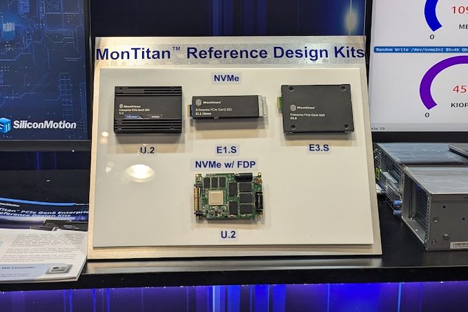
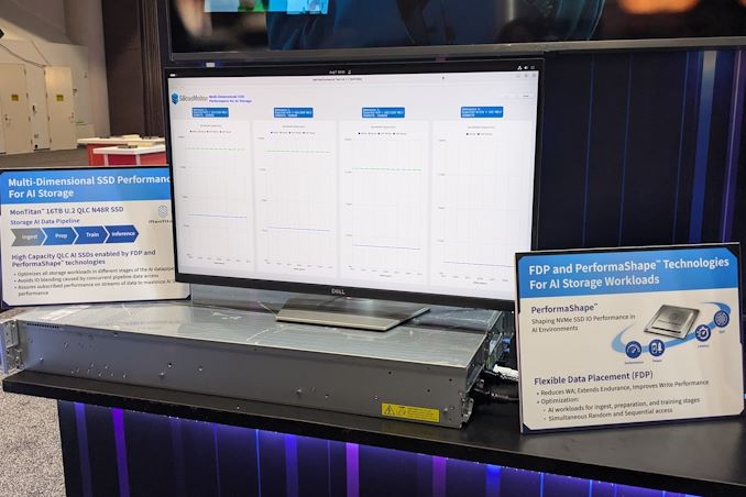
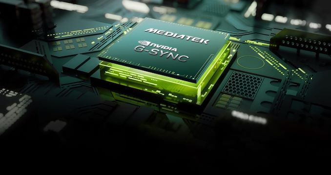

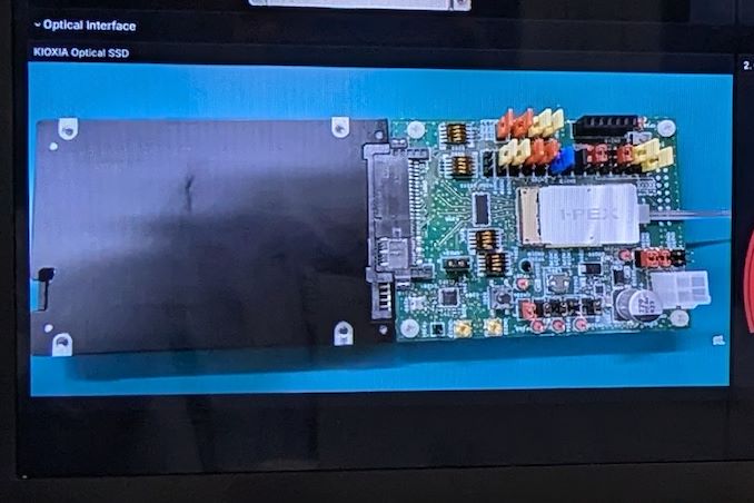
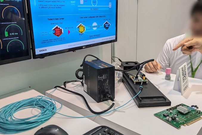
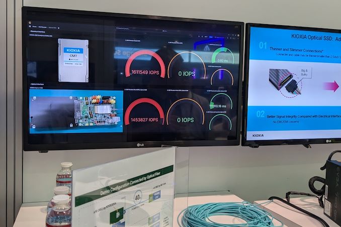
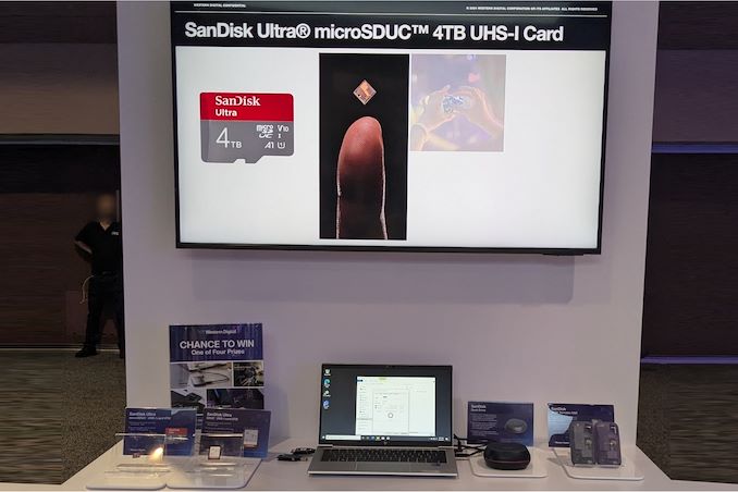
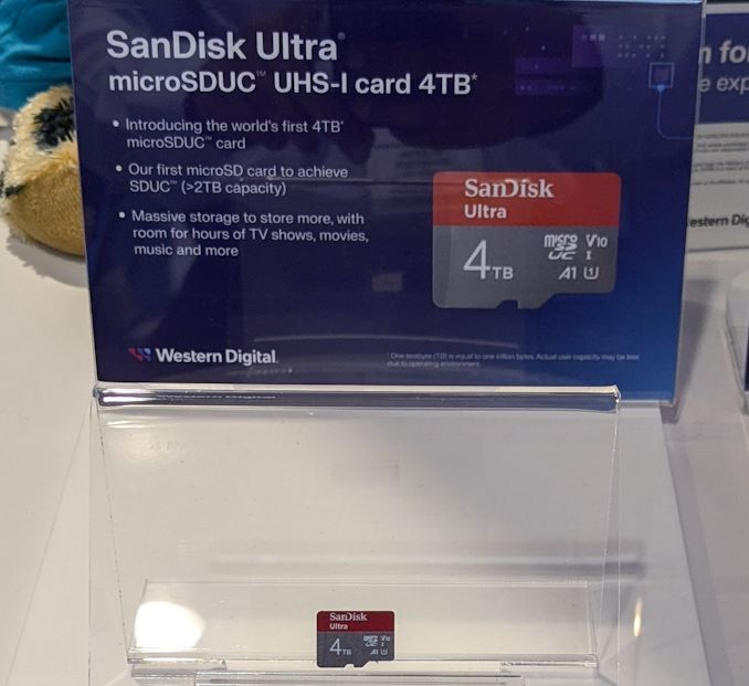

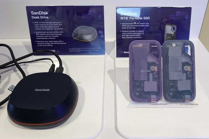

0 Comments