
The CXL consortium has had a regular presence at FMS (which rechristened itself from 'Flash Memory Summit' to the 'Future of Memory and Storage' this year). Back at FMS 2022, the company had announced v3.0 of the CXL specifications. This was followed by CXL 3.1's introduction at Supercomputing 2023. Having started off as a host to device interconnect standard, it had slowly subsumed other competing standards such as OpenCAPI and Gen-Z. As a result, the specifications started to encompass a wide variety of use-cases by building a protocol on top of the the ubiquitous PCIe expansion bus. The CXL consortium comprises of heavyweights such as AMD and Intel, as well as a large number of startup companies attempting to play in different segments on the device side. At FMS 2024, CXL had a prime position in the booth demos of many vendors.
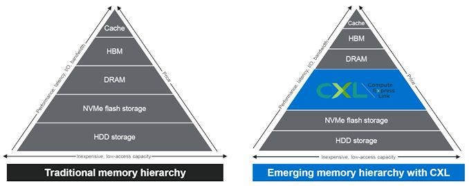
The migration of server platforms from DDR4 to DDR5, along with the rise of workloads demanding large RAM capacity (but not particularly sensitive to either memory bandwidth or latency), has opened up memory expansion modules as one of the first set of widely available CXL devices. Over the last couple of years, we have had product announcements from Samsung and Micron in this area.
At FMS 2024, SK hynix was showing off their DDR5-based CMM-DDR5 CXL memory module with a 128 GB capacity. The company was also detailing their associated Heterogeneous Memory Software Development Kit (HMSDK) - a set of libraries and tools at both the kernel and user levels aimed at increasing the ease of use of CXL memory. This is achieved in part by considering the memory pyramid / hierarchy and relocating the data between the server's main memory (DRAM) and the CXL device based on usage frequency.
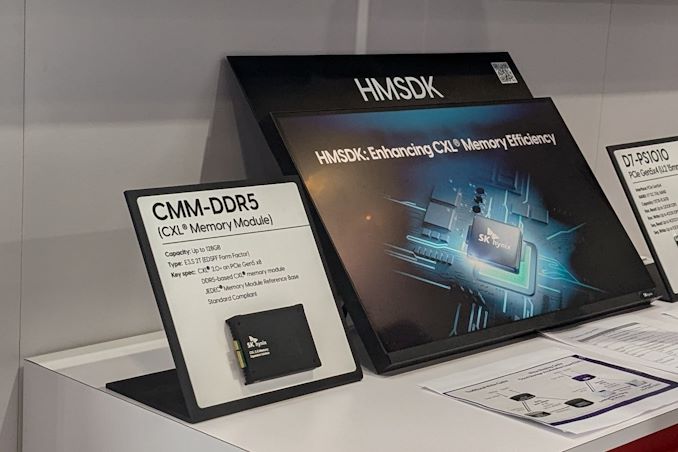
The CMM-DDR5 CXL memory module comes in the SDFF form-factor (E3.S 2T) with a PCIe 3.0 x8 host interface. The internal memory is based on 1α technology DRAM, and the device promises DDR5-class bandwidth and latency within a single NUMA hop. As these memory modules are meant to be used in datacenters and enterprises, the firmware includes features for RAS (reliability, availability, and serviceability) along with secure boot and other management features.
SK hynix was also demonstrating Niagara 2.0 - a hardware solution (currently based on FPGAs) to enable memory pooling and sharing - i.e, connecting multiple CXL memories to allow different hosts (CPUs and GPUs) to optimally share their capacity. The previous version only allowed capacity sharing, but the latest version enables sharing of data also. SK hynix had presented these solutions at the CXL DevCon 2024 earlier this year, but some progress seems to have been made in finalizing the specifications of the CMM-DDR5 at FMS 2024.
Micron had unveiled the CZ120 CXL Memory Expansion Module last year based on the Microchip SMC 2000 series CXL memory controller. At FMS 2024, Micron and Microchip had a demonstration of the module on a Granite Rapids server.
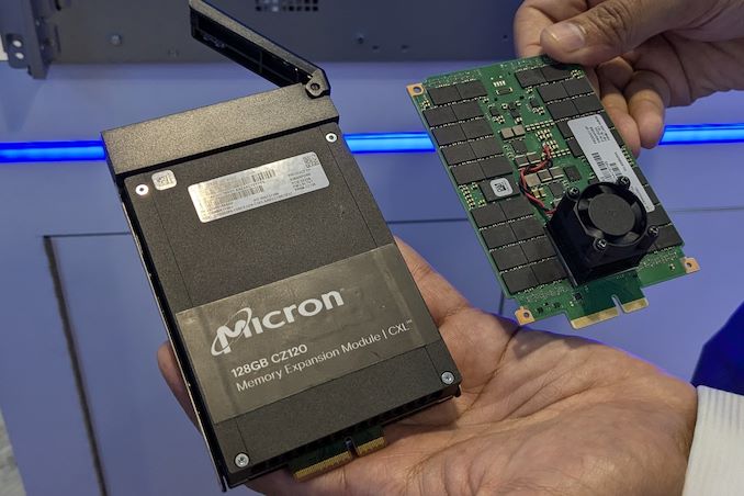
Additional insights into the SMC 2000 controller were also provided.
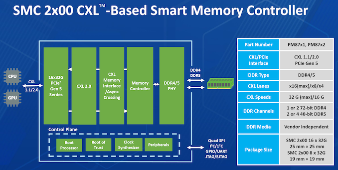
The CXL memory controller also incorporates DRAM die failure handling, and Microchip also provides diagnostics and debug tools to analyze failed modules. The memory controller also supports ECC, which forms part of the enterprise... Storage

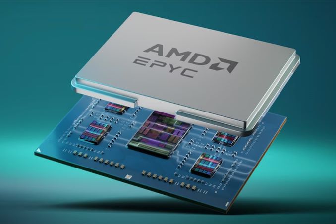
As part of AMD's Q1'2024 earnings announcement this week, the company is offering a brief status update on some of their future products set to launch later this year. Most important among these is an update on their Zen 5 CPU architecture, which is expected to launch for both client and server products later this year.
Highlighting their progress so far, AMD is confirming that EPYC "Turin" processors have begun sampling, and that these early runs of AMD's next-gen datacenter chips are meeting the company's expectations.
"Looking ahead, we are very excited about our next-gen Turin family of EPYC processors featuring our Zen 5 core," said Lisa Su, chief executive officer of AMD, at the conference call with analysts and investors (via SeekingAlpha). "We are widely sampling Turin, and the silicon is looking great. In the cloud, the significant performance and efficiency increases of Turin position us well to capture an even larger share of both first and third-party workloads."
Overall, it looks like AMD is on-track to solidify its position, and perhaps even increase its datacenter market share with its EPYC Turin processors. According to AMD, the company's server partners are developing a 30% larger number of designs for Turin than they did Genoa. This underscores how AMD's partners are preparing for even more market share growth on the back of AMD's ongoing success, not to mention the improved performance and power efficiency that the Zen 5 architecture should offer.
"In addition, there are 30% more Turin platforms in development from our server partners, compared to 4th Generation EPYC platforms, increasing our enterprise and with new solutions optimized for additional workloads," Su said. "Turin remains on track to launch later this year."
AMD's EPYC 'Turin' processors will be drop-in compatible with existing SP5 platforms (i.e., will come in an LGA 6096 package), which will facilitate its faster ramp and adoption of the platform both by cloud giants and server makers. In addition, AMD's next-generation EPYC CPUs are expected to feature more than 96 cores and a more versatile memory subsystem.
CPUs
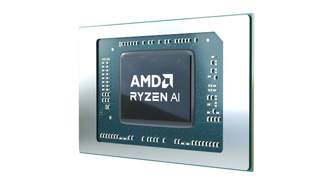
In what appears to be a mistake or a jump of the gun by ASUS, they have seemingly published a list of specifications for one of its key notebooks that all but allude to the next generation of AMD's mobile processors. While we saw AMD toy with a new nomenclature for their Phoenix silicon (Ryzen 7040 series), it seems as though AMD is once again changing things around where their naming scheme for processors is concerned.
The ASUS listing, which has now since been deleted, but as of writing is still available through Google's cache, highlights a model that is already in existence, the VivoBook S 16 OLED (M5606), but is listed with an unknown AMD Ryzen AI 9 HX 170 processor. Which, based on its specificiations, is certainly not part of the current Hawk Point (Phoenix/Phoenix 2) platform.
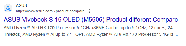
The cache on Google shows the ASUS Vivobook S 16 OLED with a Ryzen AI 9 HX 170 Processor
While it does happen in this industry occasionally, what looks like an accidental leak by ASUS on one of their product pages has unearthed an unknown processor from AMD. This first came to our attention via a post on Twitter by user @harukaze5719. While we don't speculate on rumors, we confirmed this ourselves by digging through Google's cache. Sure enough, as the image above from Google highlights, it lists a newly unannounced model of Ryzen mobile processor. Under the listing via the product compare section for the ASUS Vivobook S 16 OLED (M5606) notebook, it is listed with the AMD Ryzen AI 9 HX 170, which appears to be one of AMD's upcoming Zen 5-based mobile chips codenamed Strix Point.
So with the seemingly new nomenclature that AMD has gone with, it has a clear focus on AI, or rather Ryzen AI, by including it in the name. The Ryzen AI 9 HX 170 looks set to be a 12C/24T Zen 5 mobile variant, with their Ryzen AI NPU or similar integrated within the chip. Given that Microsoft has defined that only processors with an NPU with 45 TOPS of performance or over constitute being considered an 'AI PC', it's likely the Xilinx (now AMD Xilinx) based NPU will meet these requirements as the listing states the chip has up to 77 TOPS of AI performance available. The HX series is strikingly similar to AMD's (and Intel's) previous HX naming series for their desktop replacement SKUs for laptops, so assuming any of the details of ASUS's error are correct, then this is presumably a very high-end, high-TDP part.
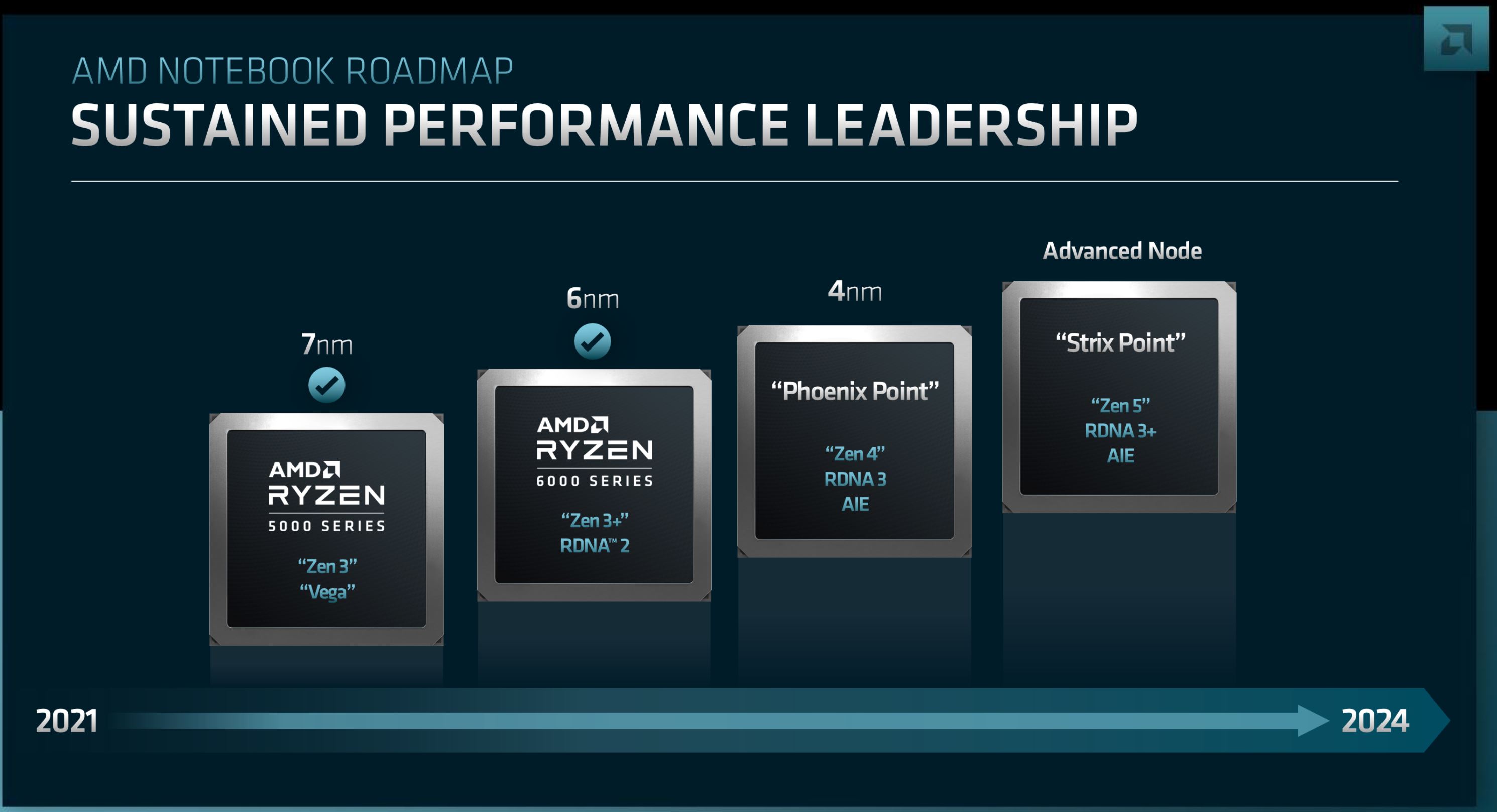
AMD Laptop Roadmap from Zen 2 in 2019 to Zen 5 on track for release in 2024
We've known for some time that AMD plans to release AMD's Zen 5-based Strix Point line-up sometime in 2024. Given the timing of Computex 2024, which is just over four weeks away, we still don't quite have the full picture of Zen 5's performance and its architectural shift over Zen 4. AMD CEO Dr. Lisa Su also confirmed that Zen 5 will come with enhanced RDNA graphics within the Strix Point SoC by stating "Strix combines our next-gen Zen 5 core with enhanced RDNA graphics and an updated Ryzen AI engine to significantly increase the performance, energy efficiency, and AI capabilities of PCs,"
While it's entirely possible as we lead up to Computex 2024 that AMD is prepared to announce more details about Zen 5, nothing is confirmed. We do know that the CEO of AMD, Dr. Lisa Su is scheduled to deliver the opening keynote of the show, Dr. Lisa Su unveiled their Zen 4 microarchitecture at Computex 2022 during AMD's keynote and even unveiled their 3D V-Cache stacking, which we know today as the Ryzen X3D CPUs back at Computex 2021.
With that in mind, AMD and Dr. Lisa Su love to announce new products and ... CPUs


A few years back, the Japanese government's New Energy and Industrial Technology Development Organization (NEDO ) allocated funding for the development of green datacenter technologies. With the aim to obtain up to 40% savings in overall power consumption, several Japanese companies have been developing an optical interface for their enterprise SSDs. And at this year's FMS, Kioxia had their optical interface on display.

For this demonstration, Kioxia took its existing CM7 enterprise SSD and created an optical interface for it. A PCIe card with on-board optics developed by Kyocera is installed in the server slot. An optical interface allows data transfer over long distances (it was 40m in the demo, but Kioxia promises lengths of up to 100m for the cable in the future). This allows the storage to be kept in a separate room with minimal cooling requirements compared to the rack with the CPUs and GPUs. Disaggregation of different server components will become an option as very high throughput interfaces such as PCIe 7.0 (with 128 GT/s rates) become available.

The demonstration of the optical SSD showed a slight loss in IOPS performance, but a significant advantage in the latency metric over the shipping enterprise SSD behind a copper network link. Obviously, there are advantages in wiring requirements and signal integrity maintenance with optical links.
Being a proof-of-concept demonstration, we do see the requirement for an industry-standard approach if this were to gain adoption among different datacenter vendors. The PCI-SIG optical workgroup will need to get its act together soon to create a standards-based approach to this problem.
Storage
A few years back, the Japanese government's New Energy and Industrial Technology Development Organization (NEDO ) allocated funding for the development of green datacenter technologies. With the aim to obtain up to 40% savings in overall power consumption, several Japanese companies have been developing an optical interface for their enterprise SSDs. And at this year's FMS, Kioxia had their optical interface on display.
For this demonstration, Kioxia took its existing CM7 enterprise SSD and created an optical interface for it. A PCIe card with on-board optics developed by Kyocera is installed in the server slot. An optical interface allows data transfer over long distances (it was 40m in the demo, but Kioxia promises lengths of up to 100m for the cable in the future). This allows the storage to be kept in a separate room with minimal cooling requirements compared to the rack with the CPUs and GPUs. Disaggregation of different server components will become an option as very high throughput interfaces such as PCIe 7.0 (with 128 GT/s rates) become available.
The demonstration of the optical SSD showed a slight loss in IOPS performance, but a significant advantage in the latency metric over the shipping enterprise SSD behind a copper network link. Obviously, there are advantages in wiring requirements and signal integrity maintenance with optical links.
Being a proof-of-concept demonstration, we do see the requirement for an industry-standard approach if this were to gain adoption among different datacenter vendors. The PCI-SIG optical workgroup will need to get its act together soon to create a standards-based approach to this problem.
Storage
As part of AMD's Q1'2024 earnings announcement this week, the company is offering a brief status update on some of their future products set to launch later this year. Most important among these is an update on their Zen 5 CPU architecture, which is expected to launch for both client and server products later this year.
Highlighting their progress so far, AMD is confirming that EPYC "Turin" processors have begun sampling, and that these early runs of AMD's next-gen datacenter chips are meeting the company's expectations.
"Looking ahead, we are very excited about our next-gen Turin family of EPYC processors featuring our Zen 5 core," said Lisa Su, chief executive officer of AMD, at the conference call with analysts and investors (via SeekingAlpha). "We are widely sampling Turin, and the silicon is looking great. In the cloud, the significant performance and efficiency increases of Turin position us well to capture an even larger share of both first and third-party workloads."
Overall, it looks like AMD is on-track to solidify its position, and perhaps even increase its datacenter market share with its EPYC Turin processors. According to AMD, the company's server partners are developing a 30% larger number of designs for Turin than they did Genoa. This underscores how AMD's partners are preparing for even more market share growth on the back of AMD's ongoing success, not to mention the improved performance and power efficiency that the Zen 5 architecture should offer.
"In addition, there are 30% more Turin platforms in development from our server partners, compared to 4th Generation EPYC platforms, increasing our enterprise and with new solutions optimized for additional workloads," Su said. "Turin remains on track to launch later this year."
AMD's EPYC 'Turin' processors will be drop-in compatible with existing SP5 platforms (i.e., will come in an LGA 6096 package), which will facilitate its faster ramp and adoption of the platform both by cloud giants and server makers. In addition, AMD's next-generation EPYC CPUs are expected to feature more than 96 cores and a more versatile memory subsystem.
CPUs
In what appears to be a mistake or a jump of the gun by ASUS, they have seemingly published a list of specifications for one of its key notebooks that all but allude to the next generation of AMD's mobile processors. While we saw AMD toy with a new nomenclature for their Phoenix silicon (Ryzen 7040 series), it seems as though AMD is once again changing things around where their naming scheme for processors is concerned.
The ASUS listing, which has now since been deleted, but as of writing is still available through Google's cache, highlights a model that is already in existence, the VivoBook S 16 OLED (M5606), but is listed with an unknown AMD Ryzen AI 9 HX 170 processor. Which, based on its specificiations, is certainly not part of the current Hawk Point (Phoenix/Phoenix 2) platform.
The cache on Google shows the ASUS Vivobook S 16 OLED with a Ryzen AI 9 HX 170 Processor
While it does happen in this industry occasionally, what looks like an accidental leak by ASUS on one of their product pages has unearthed an unknown processor from AMD. This first came to our attention via a post on Twitter by user @harukaze5719. While we don't speculate on rumors, we confirmed this ourselves by digging through Google's cache. Sure enough, as the image above from Google highlights, it lists a newly unannounced model of Ryzen mobile processor. Under the listing via the product compare section for the ASUS Vivobook S 16 OLED (M5606) notebook, it is listed with the AMD Ryzen AI 9 HX 170, which appears to be one of AMD's upcoming Zen 5-based mobile chips codenamed Strix Point.
So with the seemingly new nomenclature that AMD has gone with, it has a clear focus on AI, or rather Ryzen AI, by including it in the name. The Ryzen AI 9 HX 170 looks set to be a 12C/24T Zen 5 mobile variant, with their Ryzen AI NPU or similar integrated within the chip. Given that Microsoft has defined that only processors with an NPU with 45 TOPS of performance or over constitute being considered an 'AI PC', it's likely the Xilinx (now AMD Xilinx) based NPU will meet these requirements as the listing states the chip has up to 77 TOPS of AI performance available. The HX series is strikingly similar to AMD's (and Intel's) previous HX naming series for their desktop replacement SKUs for laptops, so assuming any of the details of ASUS's error are correct, then this is presumably a very high-end, high-TDP part.
AMD Laptop Roadmap from Zen 2 in 2019 to Zen 5 on track for release in 2024
We've known for some time that AMD plans to release AMD's Zen 5-based Strix Point line-up sometime in 2024. Given the timing of Computex 2024, which is just over four weeks away, we still don't quite have the full picture of Zen 5's performance and its architectural shift over Zen 4. AMD CEO Dr. Lisa Su also confirmed that Zen 5 will come with enhanced RDNA graphics within the Strix Point SoC by stating "Strix combines our next-gen Zen 5 core with enhanced RDNA graphics and an updated Ryzen AI engine to significantly increase the performance, energy efficiency, and AI capabilities of PCs,"
While it's entirely possible as we lead up to Computex 2024 that AMD is prepared to announce more details about Zen 5, nothing is confirmed. We do know that the CEO of AMD, Dr. Lisa Su is scheduled to deliver the opening keynote of the show, Dr. Lisa Su unveiled their Zen 4 microarchitecture at Computex 2022 during AMD's keynote and even unveiled their 3D V-Cache stacking, which we know today as the Ryzen X3D CPUs back at Computex 2021.
With that in mind, AMD and Dr. Lisa Su love to announce new products and ... CPUs
A few years back, the Japanese government's New Energy and Industrial Technology Development Organization (NEDO ) allocated funding for the development of green datacenter technologies. With the aim to obtain up to 40% savings in overall power consumption, several Japanese companies have been developing an optical interface for their enterprise SSDs. And at this year's FMS, Kioxia had their optical interface on display.
For this demonstration, Kioxia took its existing CM7 enterprise SSD and created an optical interface for it. A PCIe card with on-board optics developed by Kyocera is installed in the server slot. An optical interface allows data transfer over long distances (it was 40m in the demo, but Kioxia promises lengths of up to 100m for the cable in the future). This allows the storage to be kept in a separate room with minimal cooling requirements compared to the rack with the CPUs and GPUs. Disaggregation of different server components will become an option as very high throughput interfaces such as PCIe 7.0 (with 128 GT/s rates) become available.
The demonstration of the optical SSD showed a slight loss in IOPS performance, but a significant advantage in the latency metric over the shipping enterprise SSD behind a copper network link. Obviously, there are advantages in wiring requirements and signal integrity maintenance with optical links.
Being a proof-of-concept demonstration, we do see the requirement for an industry-standard approach if this were to gain adoption among different datacenter vendors. The PCI-SIG optical workgroup will need to get its act together soon to create a standards-based approach to this problem.
Storage
As part of AMD's Q1'2024 earnings announcement this week, the company is offering a brief status update on some of their future products set to launch later this year. Most important among these is an update on their Zen 5 CPU architecture, which is expected to launch for both client and server products later this year.
Highlighting their progress so far, AMD is confirming that EPYC "Turin" processors have begun sampling, and that these early runs of AMD's next-gen datacenter chips are meeting the company's expectations.
"Looking ahead, we are very excited about our next-gen Turin family of EPYC processors featuring our Zen 5 core," said Lisa Su, chief executive officer of AMD, at the conference call with analysts and investors (via SeekingAlpha). "We are widely sampling Turin, and the silicon is looking great. In the cloud, the significant performance and efficiency increases of Turin position us well to capture an even larger share of both first and third-party workloads."
Overall, it looks like AMD is on-track to solidify its position, and perhaps even increase its datacenter market share with its EPYC Turin processors. According to AMD, the company's server partners are developing a 30% larger number of designs for Turin than they did Genoa. This underscores how AMD's partners are preparing for even more market share growth on the back of AMD's ongoing success, not to mention the improved performance and power efficiency that the Zen 5 architecture should offer.
"In addition, there are 30% more Turin platforms in development from our server partners, compared to 4th Generation EPYC platforms, increasing our enterprise and with new solutions optimized for additional workloads," Su said. "Turin remains on track to launch later this year."
AMD's EPYC 'Turin' processors will be drop-in compatible with existing SP5 platforms (i.e., will come in an LGA 6096 package), which will facilitate its faster ramp and adoption of the platform both by cloud giants and server makers. In addition, AMD's next-generation EPYC CPUs are expected to feature more than 96 cores and a more versatile memory subsystem.
CPUs
A few years back, the Japanese government's New Energy and Industrial Technology Development Organization (NEDO ) allocated funding for the development of green datacenter technologies. With the aim to obtain up to 40% savings in overall power consumption, several Japanese companies have been developing an optical interface for their enterprise SSDs. And at this year's FMS, Kioxia had their optical interface on display.
For this demonstration, Kioxia took its existing CM7 enterprise SSD and created an optical interface for it. A PCIe card with on-board optics developed by Kyocera is installed in the server slot. An optical interface allows data transfer over long distances (it was 40m in the demo, but Kioxia promises lengths of up to 100m for the cable in the future). This allows the storage to be kept in a separate room with minimal cooling requirements compared to the rack with the CPUs and GPUs. Disaggregation of different server components will become an option as very high throughput interfaces such as PCIe 7.0 (with 128 GT/s rates) become available.
The demonstration of the optical SSD showed a slight loss in IOPS performance, but a significant advantage in the latency metric over the shipping enterprise SSD behind a copper network link. Obviously, there are advantages in wiring requirements and signal integrity maintenance with optical links.
Being a proof-of-concept demonstration, we do see the requirement for an industry-standard approach if this were to gain adoption among different datacenter vendors. The PCI-SIG optical workgroup will need to get its act together soon to create a standards-based approach to this problem.
Storage
Lorem Ipsum is simply dummy text of the printing and typesetting industry. Lorem Ipsum has been the industry's.
As part of AMD's Q1'2024 earnings announcement this week, the company is offering a brief status update on some of their future products set to launch later this year. Most important among these is an update on their Zen 5 CPU architecture, which is expected to launch for both client and server products later this year.
Highlighting their progress so far, AMD is confirming that EPYC "Turin" processors have begun sampling, and that these early runs of AMD's next-gen datacenter chips are meeting the company's expectations.
"Looking ahead, we are very excited about our next-gen Turin family of EPYC processors featuring our Zen 5 core," said Lisa Su, chief executive officer of AMD, at the conference call with analysts and investors (via SeekingAlpha). "We are widely sampling Turin, and the silicon is looking great. In the cloud, the significant performance and efficiency increases of Turin position us well to capture an even larger share of both first and third-party workloads."
Overall, it looks like AMD is on-track to solidify its position, and perhaps even increase its datacenter market share with its EPYC Turin processors. According to AMD, the company's server partners are developing a 30% larger number of designs for Turin than they did Genoa. This underscores how AMD's partners are preparing for even more market share growth on the back of AMD's ongoing success, not to mention the improved performance and power efficiency that the Zen 5 architecture should offer.
"In addition, there are 30% more Turin platforms in development from our server partners, compared to 4th Generation EPYC platforms, increasing our enterprise and with new solutions optimized for additional workloads," Su said. "Turin remains on track to launch later this year."
AMD's EPYC 'Turin' processors will be drop-in compatible with existing SP5 platforms (i.e., will come in an LGA 6096 package), which will facilitate its faster ramp and adoption of the platform both by cloud giants and server makers. In addition, AMD's next-generation EPYC CPUs are expected to feature more than 96 cores and a more versatile memory subsystem.
CPUs
In what appears to be a mistake or a jump of the gun by ASUS, they have seemingly published a list of specifications for one of its key notebooks that all but allude to the next generation of AMD's mobile processors. While we saw AMD toy with a new nomenclature for their Phoenix silicon (Ryzen 7040 series), it seems as though AMD is once again changing things around where their naming scheme for processors is concerned.
The ASUS listing, which has now since been deleted, but as of writing is still available through Google's cache, highlights a model that is already in existence, the VivoBook S 16 OLED (M5606), but is listed with an unknown AMD Ryzen AI 9 HX 170 processor. Which, based on its specificiations, is certainly not part of the current Hawk Point (Phoenix/Phoenix 2) platform.
The cache on Google shows the ASUS Vivobook S 16 OLED with a Ryzen AI 9 HX 170 Processor
While it does happen in this industry occasionally, what looks like an accidental leak by ASUS on one of their product pages has unearthed an unknown processor from AMD. This first came to our attention via a post on Twitter by user @harukaze5719. While we don't speculate on rumors, we confirmed this ourselves by digging through Google's cache. Sure enough, as the image above from Google highlights, it lists a newly unannounced model of Ryzen mobile processor. Under the listing via the product compare section for the ASUS Vivobook S 16 OLED (M5606) notebook, it is listed with the AMD Ryzen AI 9 HX 170, which appears to be one of AMD's upcoming Zen 5-based mobile chips codenamed Strix Point.
So with the seemingly new nomenclature that AMD has gone with, it has a clear focus on AI, or rather Ryzen AI, by including it in the name. The Ryzen AI 9 HX 170 looks set to be a 12C/24T Zen 5 mobile variant, with their Ryzen AI NPU or similar integrated within the chip. Given that Microsoft has defined that only processors with an NPU with 45 TOPS of performance or over constitute being considered an 'AI PC', it's likely the Xilinx (now AMD Xilinx) based NPU will meet these requirements as the listing states the chip has up to 77 TOPS of AI performance available. The HX series is strikingly similar to AMD's (and Intel's) previous HX naming series for their desktop replacement SKUs for laptops, so assuming any of the details of ASUS's error are correct, then this is presumably a very high-end, high-TDP part.
AMD Laptop Roadmap from Zen 2 in 2019 to Zen 5 on track for release in 2024
We've known for some time that AMD plans to release AMD's Zen 5-based Strix Point line-up sometime in 2024. Given the timing of Computex 2024, which is just over four weeks away, we still don't quite have the full picture of Zen 5's performance and its architectural shift over Zen 4. AMD CEO Dr. Lisa Su also confirmed that Zen 5 will come with enhanced RDNA graphics within the Strix Point SoC by stating "Strix combines our next-gen Zen 5 core with enhanced RDNA graphics and an updated Ryzen AI engine to significantly increase the performance, energy efficiency, and AI capabilities of PCs,"
While it's entirely possible as we lead up to Computex 2024 that AMD is prepared to announce more details about Zen 5, nothing is confirmed. We do know that the CEO of AMD, Dr. Lisa Su is scheduled to deliver the opening keynote of the show, Dr. Lisa Su unveiled their Zen 4 microarchitecture at Computex 2022 during AMD's keynote and even unveiled their 3D V-Cache stacking, which we know today as the Ryzen X3D CPUs back at Computex 2021.
With that in mind, AMD and Dr. Lisa Su love to announce new products and ... CPUs
A few years back, the Japanese government's New Energy and Industrial Technology Development Organization (NEDO ) allocated funding for the development of green datacenter technologies. With the aim to obtain up to 40% savings in overall power consumption, several Japanese companies have been developing an optical interface for their enterprise SSDs. And at this year's FMS, Kioxia had their optical interface on display.
For this demonstration, Kioxia took its existing CM7 enterprise SSD and created an optical interface for it. A PCIe card with on-board optics developed by Kyocera is installed in the server slot. An optical interface allows data transfer over long distances (it was 40m in the demo, but Kioxia promises lengths of up to 100m for the cable in the future). This allows the storage to be kept in a separate room with minimal cooling requirements compared to the rack with the CPUs and GPUs. Disaggregation of different server components will become an option as very high throughput interfaces such as PCIe 7.0 (with 128 GT/s rates) become available.
The demonstration of the optical SSD showed a slight loss in IOPS performance, but a significant advantage in the latency metric over the shipping enterprise SSD behind a copper network link. Obviously, there are advantages in wiring requirements and signal integrity maintenance with optical links.
Being a proof-of-concept demonstration, we do see the requirement for an industry-standard approach if this were to gain adoption among different datacenter vendors. The PCI-SIG optical workgroup will need to get its act together soon to create a standards-based approach to this problem.
Storage


. Back at FMS 2022, the company had <a href="https://www.anandtech.com/show/17520/compute-express-link-cxl-30-announced-doubled-speeds-and-flexible-fabrics">announced</a> v3.0 of the CXL specifications. This was followed by CXL 3.1's <a href="https://www.businesswire.com/news/home/20231114332690/en/CXL-Consortium-Announces-Compute-Express-Link-3.1-Specification-Release">introduction</a> at Supercomputing 2023. Having started off as a host to device interconnect standard, it had slowly <a href="https://www.anandtech.com/show/17519/">subsumed other competing standards</a> such as OpenCAPI and Gen-Z. As a result, the specifications started to encompass a wide variety of use-cases by building a protocol on top of the the ubiquitous PCIe expansion bus. The CXL consortium comprises of heavyweights such as AMD and Intel, as well as a large number of startup companies attempting to play in different segments on the device side. At FMS 2024, CXL had a prime position in the booth demos of many vendors.</p>
<p align="center"><a href="https://www.anandtech.com/show/21533/cxl-gathers-momentum-at-fms-2024"><img alt="" src="https://images.anandtech.com/doci/21533/cxl-mem-hier_575px.jpg" /></a></p>
<p>The migration of server platforms from DDR4 to DDR5, along with the rise of workloads demanding large RAM capacity (but not particularly sensitive to either memory bandwidth or latency), has opened up memory expansion modules as one of the first set of widely available CXL devices. Over the last couple of years, we have had product announcements from <a href="https://www.anandtech.com/show/21333">Samsung</a> and <a href="https://www.anandtech.com/show/20003">Micron</a> in this area.</p>
<h3>SK hynix CMM-DDR5 CXL Memory Module and HMSDK</h3>
<p>At FMS 2024, SK hynix was showing off their DDR5-based CMM-DDR5 CXL memory module with a 128 GB capacity. The company was also detailing their associated Heterogeneous Memory Software Development Kit (HMSDK) - a set of libraries and tools at both the kernel and user levels aimed at increasing the ease of use of CXL memory. This is achieved in part by considering the memory pyramid / hierarchy and relocating the data between the server's main memory (DRAM) and the CXL device based on usage frequency.</p>
<p align="center"><a href="https://www.anandtech.com/show/21533/cxl-gathers-momentum-at-fms-2024"><img alt="" src="https://images.anandtech.com/doci/21533/skh-cmm-ddr5_575px.jpg" /></a></p>
<p>The CMM-DDR5 CXL memory module comes in the SDFF form-factor (E3.S 2T) with a PCIe 3.0 x8 host interface. The internal memory is based on 1α technology DRAM, and the device promises DDR5-class bandwidth and latency within a single NUMA hop. As these memory modules are meant to be used in datacenters and enterprises, the firmware includes features for RAS (reliability, availability, and serviceability) along with secure boot and other management features.</p>
<p>SK hynix was also demonstrating Niagara 2.0 - a hardware solution (currently based on FPGAs) to enable memory pooling and sharing - i.e, connecting multiple CXL memories to allow different hosts (CPUs and GPUs) to optimally share their capacity. The previous version only allowed capacity sharing, but the latest version enables sharing of data also. SK hynix had <a href="https://news.skhynix.com/sk-hynix-presents-ai-memory-solutions-at-cxl-devcon-2024/">presented</a> these solutions at the CXL DevCon 2024 earlier this year, but some progress seems to have been made in finalizing the specifications of the CMM-DDR5 at FMS 2024.</p>
<h3>Microchip and Micron Demonstrate CZ120 CXL Memory Expansion Module</h3>
<p>Micron had <a href="https://www.anandtech.com/show/20003/">unveiled</a> the CZ120 CXL Memory Expansion Module last year based on the Microchip SMC 2000 series CXL memory controller. At FMS 2024, Micron and Microchip had a demonstration of the module on a Granite Rapids server.</p>
<p align="center"><a href="https://www.anandtech.com/show/21533/cxl-gathers-momentum-at-fms-2024"><img alt="" src="https://images.anandtech.com/doci/21533/mchip-micron_575px.jpg" /></a></p>
<p>Additional insights into the SMC 2000 controller were also provided.</p>
<p align="center"><a href="https://www.anandtech.com/show/21533/cxl-gathers-momentum-at-fms-2024"><img alt="" src="https://images.anandtech.com/doci/21533/mchip-sm2000_575px.png" /></a></p>
<p>The CXL memory controller also incorporates DRAM die failure handling, and Microchip also provides diagnostics and debug tools to analyze failed modules. The memory controller also supports ECC, which forms part of the enterprise... Storage)
. Back at FMS 2022, the company had <a href="https://www.anandtech.com/show/17520/compute-express-link-cxl-30-announced-doubled-speeds-and-flexible-fabrics">announced</a> v3.0 of the CXL specifications. This was followed by CXL 3.1's <a href="https://www.businesswire.com/news/home/20231114332690/en/CXL-Consortium-Announces-Compute-Express-Link-3.1-Specification-Release">introduction</a> at Supercomputing 2023. Having started off as a host to device interconnect standard, it had slowly <a href="https://www.anandtech.com/show/17519/">subsumed other competing standards</a> such as OpenCAPI and Gen-Z. As a result, the specifications started to encompass a wide variety of use-cases by building a protocol on top of the the ubiquitous PCIe expansion bus. The CXL consortium comprises of heavyweights such as AMD and Intel, as well as a large number of startup companies attempting to play in different segments on the device side. At FMS 2024, CXL had a prime position in the booth demos of many vendors.</p>
<p align="center"><a href="https://www.anandtech.com/show/21533/cxl-gathers-momentum-at-fms-2024"><img alt="" src="https://images.anandtech.com/doci/21533/cxl-mem-hier_575px.jpg" /></a></p>
<p>The migration of server platforms from DDR4 to DDR5, along with the rise of workloads demanding large RAM capacity (but not particularly sensitive to either memory bandwidth or latency), has opened up memory expansion modules as one of the first set of widely available CXL devices. Over the last couple of years, we have had product announcements from <a href="https://www.anandtech.com/show/21333">Samsung</a> and <a href="https://www.anandtech.com/show/20003">Micron</a> in this area.</p>
<h3>SK hynix CMM-DDR5 CXL Memory Module and HMSDK</h3>
<p>At FMS 2024, SK hynix was showing off their DDR5-based CMM-DDR5 CXL memory module with a 128 GB capacity. The company was also detailing their associated Heterogeneous Memory Software Development Kit (HMSDK) - a set of libraries and tools at both the kernel and user levels aimed at increasing the ease of use of CXL memory. This is achieved in part by considering the memory pyramid / hierarchy and relocating the data between the server's main memory (DRAM) and the CXL device based on usage frequency.</p>
<p align="center"><a href="https://www.anandtech.com/show/21533/cxl-gathers-momentum-at-fms-2024"><img alt="" src="https://images.anandtech.com/doci/21533/skh-cmm-ddr5_575px.jpg" /></a></p>
<p>The CMM-DDR5 CXL memory module comes in the SDFF form-factor (E3.S 2T) with a PCIe 3.0 x8 host interface. The internal memory is based on 1α technology DRAM, and the device promises DDR5-class bandwidth and latency within a single NUMA hop. As these memory modules are meant to be used in datacenters and enterprises, the firmware includes features for RAS (reliability, availability, and serviceability) along with secure boot and other management features.</p>
<p>SK hynix was also demonstrating Niagara 2.0 - a hardware solution (currently based on FPGAs) to enable memory pooling and sharing - i.e, connecting multiple CXL memories to allow different hosts (CPUs and GPUs) to optimally share their capacity. The previous version only allowed capacity sharing, but the latest version enables sharing of data also. SK hynix had <a href="https://news.skhynix.com/sk-hynix-presents-ai-memory-solutions-at-cxl-devcon-2024/">presented</a> these solutions at the CXL DevCon 2024 earlier this year, but some progress seems to have been made in finalizing the specifications of the CMM-DDR5 at FMS 2024.</p>
<h3>Microchip and Micron Demonstrate CZ120 CXL Memory Expansion Module</h3>
<p>Micron had <a href="https://www.anandtech.com/show/20003/">unveiled</a> the CZ120 CXL Memory Expansion Module last year based on the Microchip SMC 2000 series CXL memory controller. At FMS 2024, Micron and Microchip had a demonstration of the module on a Granite Rapids server.</p>
<p align="center"><a href="https://www.anandtech.com/show/21533/cxl-gathers-momentum-at-fms-2024"><img alt="" src="https://images.anandtech.com/doci/21533/mchip-micron_575px.jpg" /></a></p>
<p>Additional insights into the SMC 2000 controller were also provided.</p>
<p align="center"><a href="https://www.anandtech.com/show/21533/cxl-gathers-momentum-at-fms-2024"><img alt="" src="https://images.anandtech.com/doci/21533/mchip-sm2000_575px.png" /></a></p>
<p>The CXL memory controller also incorporates DRAM die failure handling, and Microchip also provides diagnostics and debug tools to analyze failed modules. The memory controller also supports ECC, which forms part of the enterprise... Storage | https://compbuddey.blogspot.com/2025/04/cxl-gathers-momentum-at-fms-2024-cxl_18.html)
. Back at FMS 2022, the company had <a href="https://www.anandtech.com/show/17520/compute-express-link-cxl-30-announced-doubled-speeds-and-flexible-fabrics">announced</a> v3.0 of the CXL specifications. This was followed by CXL 3.1's <a href="https://www.businesswire.com/news/home/20231114332690/en/CXL-Consortium-Announces-Compute-Express-Link-3.1-Specification-Release">introduction</a> at Supercomputing 2023. Having started off as a host to device interconnect standard, it had slowly <a href="https://www.anandtech.com/show/17519/">subsumed other competing standards</a> such as OpenCAPI and Gen-Z. As a result, the specifications started to encompass a wide variety of use-cases by building a protocol on top of the the ubiquitous PCIe expansion bus. The CXL consortium comprises of heavyweights such as AMD and Intel, as well as a large number of startup companies attempting to play in different segments on the device side. At FMS 2024, CXL had a prime position in the booth demos of many vendors.</p>
<p align="center"><a href="https://www.anandtech.com/show/21533/cxl-gathers-momentum-at-fms-2024"><img alt="" src="https://images.anandtech.com/doci/21533/cxl-mem-hier_575px.jpg" /></a></p>
<p>The migration of server platforms from DDR4 to DDR5, along with the rise of workloads demanding large RAM capacity (but not particularly sensitive to either memory bandwidth or latency), has opened up memory expansion modules as one of the first set of widely available CXL devices. Over the last couple of years, we have had product announcements from <a href="https://www.anandtech.com/show/21333">Samsung</a> and <a href="https://www.anandtech.com/show/20003">Micron</a> in this area.</p>
<h3>SK hynix CMM-DDR5 CXL Memory Module and HMSDK</h3>
<p>At FMS 2024, SK hynix was showing off their DDR5-based CMM-DDR5 CXL memory module with a 128 GB capacity. The company was also detailing their associated Heterogeneous Memory Software Development Kit (HMSDK) - a set of libraries and tools at both the kernel and user levels aimed at increasing the ease of use of CXL memory. This is achieved in part by considering the memory pyramid / hierarchy and relocating the data between the server's main memory (DRAM) and the CXL device based on usage frequency.</p>
<p align="center"><a href="https://www.anandtech.com/show/21533/cxl-gathers-momentum-at-fms-2024"><img alt="" src="https://images.anandtech.com/doci/21533/skh-cmm-ddr5_575px.jpg" /></a></p>
<p>The CMM-DDR5 CXL memory module comes in the SDFF form-factor (E3.S 2T) with a PCIe 3.0 x8 host interface. The internal memory is based on 1α technology DRAM, and the device promises DDR5-class bandwidth and latency within a single NUMA hop. As these memory modules are meant to be used in datacenters and enterprises, the firmware includes features for RAS (reliability, availability, and serviceability) along with secure boot and other management features.</p>
<p>SK hynix was also demonstrating Niagara 2.0 - a hardware solution (currently based on FPGAs) to enable memory pooling and sharing - i.e, connecting multiple CXL memories to allow different hosts (CPUs and GPUs) to optimally share their capacity. The previous version only allowed capacity sharing, but the latest version enables sharing of data also. SK hynix had <a href="https://news.skhynix.com/sk-hynix-presents-ai-memory-solutions-at-cxl-devcon-2024/">presented</a> these solutions at the CXL DevCon 2024 earlier this year, but some progress seems to have been made in finalizing the specifications of the CMM-DDR5 at FMS 2024.</p>
<h3>Microchip and Micron Demonstrate CZ120 CXL Memory Expansion Module</h3>
<p>Micron had <a href="https://www.anandtech.com/show/20003/">unveiled</a> the CZ120 CXL Memory Expansion Module last year based on the Microchip SMC 2000 series CXL memory controller. At FMS 2024, Micron and Microchip had a demonstration of the module on a Granite Rapids server.</p>
<p align="center"><a href="https://www.anandtech.com/show/21533/cxl-gathers-momentum-at-fms-2024"><img alt="" src="https://images.anandtech.com/doci/21533/mchip-micron_575px.jpg" /></a></p>
<p>Additional insights into the SMC 2000 controller were also provided.</p>
<p align="center"><a href="https://www.anandtech.com/show/21533/cxl-gathers-momentum-at-fms-2024"><img alt="" src="https://images.anandtech.com/doci/21533/mchip-sm2000_575px.png" /></a></p>
<p>The CXL memory controller also incorporates DRAM die failure handling, and Microchip also provides diagnostics and debug tools to analyze failed modules. The memory controller also supports ECC, which forms part of the enterprise... Storage&body=https://compbuddey.blogspot.com/2025/04/cxl-gathers-momentum-at-fms-2024-cxl_18.html)
0 Comments