PCI-SIG Demonstrates PCIe 6.0 Interoperability at FMS 2024 <p align="center"><a href="https://www.anandtech.com/show/21531/pcisig-demonstrates-pcie-60-interoperability-at-fms-2024"><img src="https://images.anandtech.com/doci/21531/pci-sig-carousel_575px.jpg" alt="" /></a></p><p><p>As the deployment of PCIe 5.0 picks up steam in both datacenter and consumer markets, PCI-SIG is not sitting idle, and is already working on getting the ecosystem ready for the updats to the PCIe specifications. At FMS 2024, some vendors were even talking about PCIe 7.0 with its 128 GT/s capabilities despite PCIe 6.0 not even starting to ship yet. We caught up with PCI-SIG to get some updates on its activities and have a discussion on the current state of the PCIe ecosystem.</p>
<p align="center"><a href="https://www.anandtech.com/show/21531/pcisig-demonstrates-pcie-60-interoperability-at-fms-2024"><img alt="" src="https://images.anandtech.com/doci/21531/pci-sig-roadmap_575px.jpg" /></a></p>
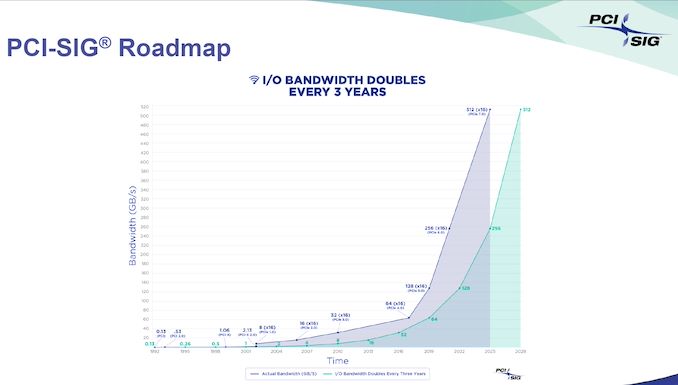
<p>PCI-SIG has already made the PCIe 7.0 specifications (v 0.5) available to its members, and expects full specifications to be officially released sometime in 2025. The goal is to deliver a 128 GT/s data rate with up to 512 GBps of bidirectional traffic using x16 links. Similar to PCIe 6.0, this specification will also utilize PAM4 signaling and maintain backwards compatibility. Power efficiency as well as silicon die area are also being kept in mind as part of the drafting process.</p>
<p align="center"><a href="https://www.anandtech.com/show/21531/pcisig-demonstrates-pcie-60-interoperability-at-fms-2024"><img alt="" src="https://images.anandtech.com/doci/21531/pcie-char_575px.jpg" /></a></p>
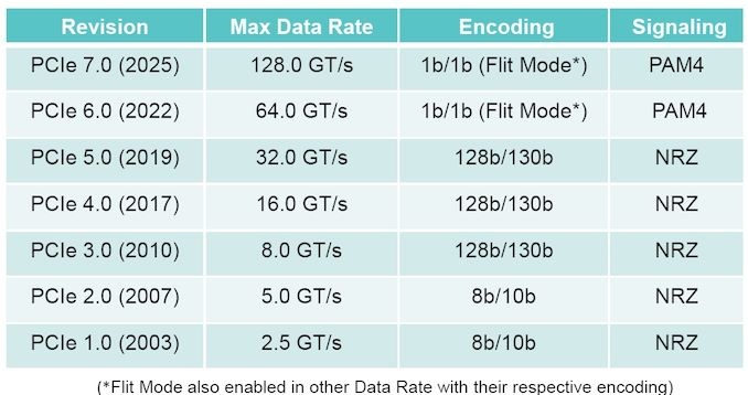
<p>The move to PAM4 signaling brings higher bit-error rates compared to the previous NRZ scheme. This made it necessary to adopt a different error correction scheme in PCIe 6.0 - instead of operating on variable length packets, PCIe 6.0's Flow Control Unit (FLIT) encoding operates on fixed size packets to aid in forward error correction. PCIe 7.0 retains these aspects.</p>
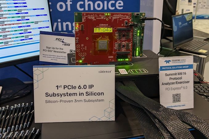
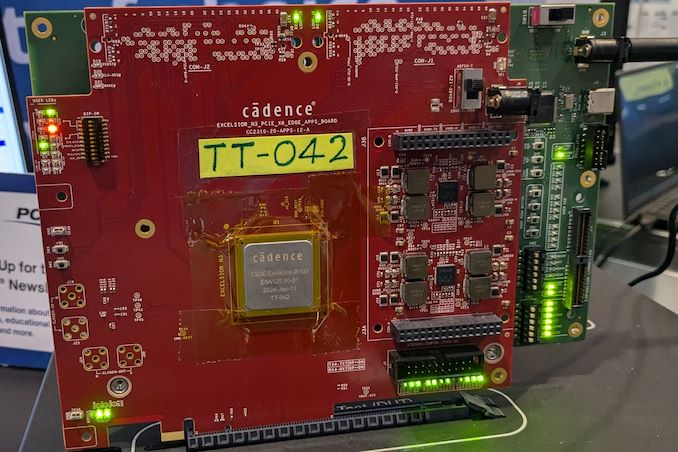
<p>The integrators list for the PCIe 6.0 compliance program is also expected to come out in 2025, though initial testing is already in progress. This was evident by the FMS 2024 demo involving Cadence's 3nm test chip for its PCIe 6.0 IP offering along with Teledyne Lecroy's PCIe 6.0 analyzer. These timelines track well with the specification completion dates and compliance program availability for previous PCIe generations.</p>
<p align="center"><a href="https://www.anandtech.com/show/21531/pcisig-demonstrates-pcie-60-interoperability-at-fms-2024"><img alt="" src="https://images.anandtech.com/doci/21531/pcie-cadence_575px.jpg" /></a></p>
<p>We also received an update on the optical workgroup - while being optical-technology agnostic, the WG also intends to develop technology-specific form-factors including pluggable optical transceivers, on-board optics, co-packaged optics, and optical I/O. The logical and electrical layers of the PCIe 6.0 specifications are being enhanced to accommodate the new optical PCIe standardization and this process will also be done with PCIe 7.0 to coincide with that standard's release next year.</p>
<p align="center"><a href="https://www.anandtech.com/show/21531/pcisig-demonstrates-pcie-60-interoperability-at-fms-2024"><img alt="" src="https://images.anandtech.com/doci/21531/pcie-cabling_575px.jpg" /></a></p>
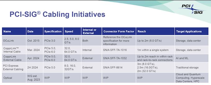
<p>The PCI-SIG also has ongoing cabling initiatives. On the consumer side, we have seen significant traction for Thunderbolt and external GPU enclosures. However, even datacenters and enterprise systems are moving towards cabling solutions as it becomes evident that disaggregation of components such as storage from the CPU and GPU are better for thermal design. Additionally maintaining signal integrity over longer distances becomes difficult for on-board signal traces. Cabling internal to the computing systems can help here.</p>
<p>OCuLink emerged as a good candidate and was adopted fairly widely as an internal link in server systems. It has even made an appearance in mini-PCs from some Chinese manufacturers in its external avatar for the consumer market, albeit with limited traction. As speeds increase, a widely-adopted standard for external PCIe peripherals (or even connecting components within a system) will become imperative.</p>
</p> Storage
PCI-SIG Demonstrates PCIe 6.0 Interoperability at FMS 2024
As the deployment of PCIe 5.0 picks up steam in both datacenter and consumer markets, PCI-SIG is not sitting idle, and is already working on getting the ecosystem ready for the updats to the PCIe specifications. At FMS 2024, some vendors were even talking about PCIe 7.0 with its 128 GT/s capabilities despite PCIe 6.0 not even starting to ship yet. We caught up with PCI-SIG to get some updates on its activities and have a discussion on the current state of the PCIe ecosystem.
PCI-SIG has already made the PCIe 7.0 specifications (v 0.5) available to its members, and expects full specifications to be officially released sometime in 2025. The goal is to deliver a 128 GT/s data rate with up to 512 GBps of bidirectional traffic using x16 links. Similar to PCIe 6.0, this specification will also utilize PAM4 signaling and maintain backwards compatibility. Power efficiency as well as silicon die area are also being kept in mind as part of the drafting process.
The move to PAM4 signaling brings higher bit-error rates compared to the previous NRZ scheme. This made it necessary to adopt a different error correction scheme in PCIe 6.0 - instead of operating on variable length packets, PCIe 6.0's Flow Control Unit (FLIT) encoding operates on fixed size packets to aid in forward error correction. PCIe 7.0 retains these aspects.
The integrators list for the PCIe 6.0 compliance program is also expected to come out in 2025, though initial testing is already in progress. This was evident by the FMS 2024 demo involving Cadence's 3nm test chip for its PCIe 6.0 IP offering along with Teledyne Lecroy's PCIe 6.0 analyzer. These timelines track well with the specification completion dates and compliance program availability for previous PCIe generations.
We also received an update on the optical workgroup - while being optical-technology agnostic, the WG also intends to develop technology-specific form-factors including pluggable optical transceivers, on-board optics, co-packaged optics, and optical I/O. The logical and electrical layers of the PCIe 6.0 specifications are being enhanced to accommodate the new optical PCIe standardization and this process will also be done with PCIe 7.0 to coincide with that standard's release next year.
The PCI-SIG also has ongoing cabling initiatives. On the consumer side, we have seen significant traction for Thunderbolt and external GPU enclosures. However, even datacenters and enterprise systems are moving towards cabling solutions as it becomes evident that disaggregation of components such as storage from the CPU and GPU are better for thermal design. Additionally maintaining signal integrity over longer distances becomes difficult for on-board signal traces. Cabling internal to the computing systems can help here.
OCuLink emerged as a good candidate and was adopted fairly widely as an internal link in server systems. It has even made an appearance in mini-PCs from some Chinese manufacturers in its external avatar for the consumer market, albeit with limited traction. As speeds increase, a widely-adopted standard for external PCIe peripherals (or even connecting components within a system) will become imperative.


 available to its members, and expects full specifications to be officially released sometime in 2025. The goal is to deliver a 128 GT/s data rate with up to 512 GBps of bidirectional traffic using x16 links. Similar to PCIe 6.0, this specification will also utilize PAM4 signaling and maintain backwards compatibility. Power efficiency as well as silicon die area are also being kept in mind as part of the drafting process.</p>
<p align="center"><a href="https://www.anandtech.com/show/21531/pcisig-demonstrates-pcie-60-interoperability-at-fms-2024"><img alt="" src="https://images.anandtech.com/doci/21531/pcie-char_575px.jpg" /></a></p>
<p>The move to PAM4 signaling brings higher bit-error rates compared to the previous NRZ scheme. This made it necessary to adopt a different error correction scheme in PCIe 6.0 - instead of operating on variable length packets, PCIe 6.0's Flow Control Unit (FLIT) encoding operates on fixed size packets to aid in forward error correction. PCIe 7.0 retains these aspects.</p>
<p>The integrators list for the PCIe 6.0 compliance program is also expected to come out in 2025, though initial testing is already in progress. This was evident by the FMS 2024 demo involving Cadence's 3nm test chip for its PCIe 6.0 IP offering along with Teledyne Lecroy's PCIe 6.0 analyzer. These timelines track well with the specification completion dates and compliance program availability for previous PCIe generations.</p>
<p align="center"><a href="https://www.anandtech.com/show/21531/pcisig-demonstrates-pcie-60-interoperability-at-fms-2024"><img alt="" src="https://images.anandtech.com/doci/21531/pcie-cadence_575px.jpg" /></a></p>
<p>We also received an update on the optical workgroup - while being optical-technology agnostic, the WG also intends to develop technology-specific form-factors including pluggable optical transceivers, on-board optics, co-packaged optics, and optical I/O. The logical and electrical layers of the PCIe 6.0 specifications are being enhanced to accommodate the new optical PCIe standardization and this process will also be done with PCIe 7.0 to coincide with that standard's release next year.</p>
<p align="center"><a href="https://www.anandtech.com/show/21531/pcisig-demonstrates-pcie-60-interoperability-at-fms-2024"><img alt="" src="https://images.anandtech.com/doci/21531/pcie-cabling_575px.jpg" /></a></p>
<p>The PCI-SIG also has ongoing cabling initiatives. On the consumer side, we have seen significant traction for Thunderbolt and external GPU enclosures. However, even datacenters and enterprise systems are moving towards cabling solutions as it becomes evident that disaggregation of components such as storage from the CPU and GPU are better for thermal design. Additionally maintaining signal integrity over longer distances becomes difficult for on-board signal traces. Cabling internal to the computing systems can help here.</p>
<p>OCuLink emerged as a good candidate and was adopted fairly widely as an internal link in server systems. It has even made an appearance in mini-PCs from some Chinese manufacturers in its external avatar for the consumer market, albeit with limited traction. As speeds increase, a widely-adopted standard for external PCIe peripherals (or even connecting components within a system) will become imperative.</p>
</p> Storage)
 available to its members, and expects full specifications to be officially released sometime in 2025. The goal is to deliver a 128 GT/s data rate with up to 512 GBps of bidirectional traffic using x16 links. Similar to PCIe 6.0, this specification will also utilize PAM4 signaling and maintain backwards compatibility. Power efficiency as well as silicon die area are also being kept in mind as part of the drafting process.</p>
<p align="center"><a href="https://www.anandtech.com/show/21531/pcisig-demonstrates-pcie-60-interoperability-at-fms-2024"><img alt="" src="https://images.anandtech.com/doci/21531/pcie-char_575px.jpg" /></a></p>
<p>The move to PAM4 signaling brings higher bit-error rates compared to the previous NRZ scheme. This made it necessary to adopt a different error correction scheme in PCIe 6.0 - instead of operating on variable length packets, PCIe 6.0's Flow Control Unit (FLIT) encoding operates on fixed size packets to aid in forward error correction. PCIe 7.0 retains these aspects.</p>
<p>The integrators list for the PCIe 6.0 compliance program is also expected to come out in 2025, though initial testing is already in progress. This was evident by the FMS 2024 demo involving Cadence's 3nm test chip for its PCIe 6.0 IP offering along with Teledyne Lecroy's PCIe 6.0 analyzer. These timelines track well with the specification completion dates and compliance program availability for previous PCIe generations.</p>
<p align="center"><a href="https://www.anandtech.com/show/21531/pcisig-demonstrates-pcie-60-interoperability-at-fms-2024"><img alt="" src="https://images.anandtech.com/doci/21531/pcie-cadence_575px.jpg" /></a></p>
<p>We also received an update on the optical workgroup - while being optical-technology agnostic, the WG also intends to develop technology-specific form-factors including pluggable optical transceivers, on-board optics, co-packaged optics, and optical I/O. The logical and electrical layers of the PCIe 6.0 specifications are being enhanced to accommodate the new optical PCIe standardization and this process will also be done with PCIe 7.0 to coincide with that standard's release next year.</p>
<p align="center"><a href="https://www.anandtech.com/show/21531/pcisig-demonstrates-pcie-60-interoperability-at-fms-2024"><img alt="" src="https://images.anandtech.com/doci/21531/pcie-cabling_575px.jpg" /></a></p>
<p>The PCI-SIG also has ongoing cabling initiatives. On the consumer side, we have seen significant traction for Thunderbolt and external GPU enclosures. However, even datacenters and enterprise systems are moving towards cabling solutions as it becomes evident that disaggregation of components such as storage from the CPU and GPU are better for thermal design. Additionally maintaining signal integrity over longer distances becomes difficult for on-board signal traces. Cabling internal to the computing systems can help here.</p>
<p>OCuLink emerged as a good candidate and was adopted fairly widely as an internal link in server systems. It has even made an appearance in mini-PCs from some Chinese manufacturers in its external avatar for the consumer market, albeit with limited traction. As speeds increase, a widely-adopted standard for external PCIe peripherals (or even connecting components within a system) will become imperative.</p>
</p> Storage | https://compbuddey.blogspot.com/2025/03/pci-sig-demonstrates-pcie-60.html)
 available to its members, and expects full specifications to be officially released sometime in 2025. The goal is to deliver a 128 GT/s data rate with up to 512 GBps of bidirectional traffic using x16 links. Similar to PCIe 6.0, this specification will also utilize PAM4 signaling and maintain backwards compatibility. Power efficiency as well as silicon die area are also being kept in mind as part of the drafting process.</p>
<p align="center"><a href="https://www.anandtech.com/show/21531/pcisig-demonstrates-pcie-60-interoperability-at-fms-2024"><img alt="" src="https://images.anandtech.com/doci/21531/pcie-char_575px.jpg" /></a></p>
<p>The move to PAM4 signaling brings higher bit-error rates compared to the previous NRZ scheme. This made it necessary to adopt a different error correction scheme in PCIe 6.0 - instead of operating on variable length packets, PCIe 6.0's Flow Control Unit (FLIT) encoding operates on fixed size packets to aid in forward error correction. PCIe 7.0 retains these aspects.</p>
<p>The integrators list for the PCIe 6.0 compliance program is also expected to come out in 2025, though initial testing is already in progress. This was evident by the FMS 2024 demo involving Cadence's 3nm test chip for its PCIe 6.0 IP offering along with Teledyne Lecroy's PCIe 6.0 analyzer. These timelines track well with the specification completion dates and compliance program availability for previous PCIe generations.</p>
<p align="center"><a href="https://www.anandtech.com/show/21531/pcisig-demonstrates-pcie-60-interoperability-at-fms-2024"><img alt="" src="https://images.anandtech.com/doci/21531/pcie-cadence_575px.jpg" /></a></p>
<p>We also received an update on the optical workgroup - while being optical-technology agnostic, the WG also intends to develop technology-specific form-factors including pluggable optical transceivers, on-board optics, co-packaged optics, and optical I/O. The logical and electrical layers of the PCIe 6.0 specifications are being enhanced to accommodate the new optical PCIe standardization and this process will also be done with PCIe 7.0 to coincide with that standard's release next year.</p>
<p align="center"><a href="https://www.anandtech.com/show/21531/pcisig-demonstrates-pcie-60-interoperability-at-fms-2024"><img alt="" src="https://images.anandtech.com/doci/21531/pcie-cabling_575px.jpg" /></a></p>
<p>The PCI-SIG also has ongoing cabling initiatives. On the consumer side, we have seen significant traction for Thunderbolt and external GPU enclosures. However, even datacenters and enterprise systems are moving towards cabling solutions as it becomes evident that disaggregation of components such as storage from the CPU and GPU are better for thermal design. Additionally maintaining signal integrity over longer distances becomes difficult for on-board signal traces. Cabling internal to the computing systems can help here.</p>
<p>OCuLink emerged as a good candidate and was adopted fairly widely as an internal link in server systems. It has even made an appearance in mini-PCs from some Chinese manufacturers in its external avatar for the consumer market, albeit with limited traction. As speeds increase, a widely-adopted standard for external PCIe peripherals (or even connecting components within a system) will become imperative.</p>
</p> Storage&body=https://compbuddey.blogspot.com/2025/03/pci-sig-demonstrates-pcie-60.html)
0 Comments