

NVIDIA on Tuesday said that future monitor scalers from MediaTek will support its G-Sync technologies. NVIDIA is partnering with MediaTek to integrate its full range of G-Sync technologies into future monitors without requiring a standalone G-Sync module, which makes advanced gaming features more accessible across a broader range of displays.
Traditionally, G-Sync technology relied on a dedicated G-sync module – based on an Altera FPGA – to handle syncing display refresh rates with the GPU in order to reduce screen tearing, stutter, and input lag. As a more basic solution, in 2019 NVIDIA introduced G-Sync Compatible certification and branding, which leveraged the industry-standard VESA AdaptiveSync technology to handle variable refresh rates. In lieu of using a dedicated module, leveraging AdaptiveSync allowed for cheaper monitors, with NVIDIA's program serving as a stamp of approval that the monitor worked with NVIDIA GPUs and met NVIDIA's performance requirements. Still, G-Sync Compatible monitors still lack some features that, to date, require the dedicated G-Sync module.
Through this new partnership with MediaTek, MediaTek will bring support for all of NVIDIA's G-Sync technologies, including the latest G-Sync Pulsar, directly into their scalers. G-Sync Pulsar enhances motion clarity and reduces ghosting, providing a smoother gaming experience. In addition to variable refresh rates and Pulsar, MediaTek-based G-Sync displays will support such features as variable overdrive, 12-bit color, Ultra Low Motion Blur, low latency HDR, and Reflex Analyzer. This integration will allow more monitors to support a full range of G-Sync features without having to incorporate an expensive FPGA.
The first monitors to feature full G-Sync support without needing an NVIDIA module include the AOC Agon Pro AG276QSG2, Acer Predator XB273U F5, and ASUS ROG Swift 360Hz PG27AQNR. These monitors offer 360Hz refresh rates, 1440p resolution, and HDR support.
What remains to be seen is which specific MediaTek's scalers will support NVIDIA's G-Sync technology – or if the company is going to implement support into all of their scalers going forward. It also remains to be seen whether monitors with NVIDIA's dedicated G-Sync modules retain any advantages over displays with MediaTek's scalers.
Monitors
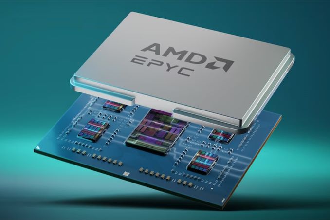
As part of AMD's Q1'2024 earnings announcement this week, the company is offering a brief status update on some of their future products set to launch later this year. Most important among these is an update on their Zen 5 CPU architecture, which is expected to launch for both client and server products later this year.
Highlighting their progress so far, AMD is confirming that EPYC "Turin" processors have begun sampling, and that these early runs of AMD's next-gen datacenter chips are meeting the company's expectations.
"Looking ahead, we are very excited about our next-gen Turin family of EPYC processors featuring our Zen 5 core," said Lisa Su, chief executive officer of AMD, at the conference call with analysts and investors (via SeekingAlpha). "We are widely sampling Turin, and the silicon is looking great. In the cloud, the significant performance and efficiency increases of Turin position us well to capture an even larger share of both first and third-party workloads."
Overall, it looks like AMD is on-track to solidify its position, and perhaps even increase its datacenter market share with its EPYC Turin processors. According to AMD, the company's server partners are developing a 30% larger number of designs for Turin than they did Genoa. This underscores how AMD's partners are preparing for even more market share growth on the back of AMD's ongoing success, not to mention the improved performance and power efficiency that the Zen 5 architecture should offer.
"In addition, there are 30% more Turin platforms in development from our server partners, compared to 4th Generation EPYC platforms, increasing our enterprise and with new solutions optimized for additional workloads," Su said. "Turin remains on track to launch later this year."
AMD's EPYC 'Turin' processors will be drop-in compatible with existing SP5 platforms (i.e., will come in an LGA 6096 package), which will facilitate its faster ramp and adoption of the platform both by cloud giants and server makers. In addition, AMD's next-generation EPYC CPUs are expected to feature more than 96 cores and a more versatile memory subsystem.
CPUs

A few years back, the Japanese government's New Energy and Industrial Technology Development Organization (NEDO ) allocated funding for the development of green datacenter technologies. With the aim to obtain up to 40% savings in overall power consumption, several Japanese companies have been developing an optical interface for their enterprise SSDs. And at this year's FMS, Kioxia had their optical interface on display.

For this demonstration, Kioxia took its existing CM7 enterprise SSD and created an optical interface for it. A PCIe card with on-board optics developed by Kyocera is installed in the server slot. An optical interface allows data transfer over long distances (it was 40m in the demo, but Kioxia promises lengths of up to 100m for the cable in the future). This allows the storage to be kept in a separate room with minimal cooling requirements compared to the rack with the CPUs and GPUs. Disaggregation of different server components will become an option as very high throughput interfaces such as PCIe 7.0 (with 128 GT/s rates) become available.

The demonstration of the optical SSD showed a slight loss in IOPS performance, but a significant advantage in the latency metric over the shipping enterprise SSD behind a copper network link. Obviously, there are advantages in wiring requirements and signal integrity maintenance with optical links.
Being a proof-of-concept demonstration, we do see the requirement for an industry-standard approach if this were to gain adoption among different datacenter vendors. The PCI-SIG optical workgroup will need to get its act together soon to create a standards-based approach to this problem.
Storage
A few years back, the Japanese government's New Energy and Industrial Technology Development Organization (NEDO ) allocated funding for the development of green datacenter technologies. With the aim to obtain up to 40% savings in overall power consumption, several Japanese companies have been developing an optical interface for their enterprise SSDs. And at this year's FMS, Kioxia had their optical interface on display.
For this demonstration, Kioxia took its existing CM7 enterprise SSD and created an optical interface for it. A PCIe card with on-board optics developed by Kyocera is installed in the server slot. An optical interface allows data transfer over long distances (it was 40m in the demo, but Kioxia promises lengths of up to 100m for the cable in the future). This allows the storage to be kept in a separate room with minimal cooling requirements compared to the rack with the CPUs and GPUs. Disaggregation of different server components will become an option as very high throughput interfaces such as PCIe 7.0 (with 128 GT/s rates) become available.
The demonstration of the optical SSD showed a slight loss in IOPS performance, but a significant advantage in the latency metric over the shipping enterprise SSD behind a copper network link. Obviously, there are advantages in wiring requirements and signal integrity maintenance with optical links.
Being a proof-of-concept demonstration, we do see the requirement for an industry-standard approach if this were to gain adoption among different datacenter vendors. The PCI-SIG optical workgroup will need to get its act together soon to create a standards-based approach to this problem.
Storage
As part of AMD's Q1'2024 earnings announcement this week, the company is offering a brief status update on some of their future products set to launch later this year. Most important among these is an update on their Zen 5 CPU architecture, which is expected to launch for both client and server products later this year.
Highlighting their progress so far, AMD is confirming that EPYC "Turin" processors have begun sampling, and that these early runs of AMD's next-gen datacenter chips are meeting the company's expectations.
"Looking ahead, we are very excited about our next-gen Turin family of EPYC processors featuring our Zen 5 core," said Lisa Su, chief executive officer of AMD, at the conference call with analysts and investors (via SeekingAlpha). "We are widely sampling Turin, and the silicon is looking great. In the cloud, the significant performance and efficiency increases of Turin position us well to capture an even larger share of both first and third-party workloads."
Overall, it looks like AMD is on-track to solidify its position, and perhaps even increase its datacenter market share with its EPYC Turin processors. According to AMD, the company's server partners are developing a 30% larger number of designs for Turin than they did Genoa. This underscores how AMD's partners are preparing for even more market share growth on the back of AMD's ongoing success, not to mention the improved performance and power efficiency that the Zen 5 architecture should offer.
"In addition, there are 30% more Turin platforms in development from our server partners, compared to 4th Generation EPYC platforms, increasing our enterprise and with new solutions optimized for additional workloads," Su said. "Turin remains on track to launch later this year."
AMD's EPYC 'Turin' processors will be drop-in compatible with existing SP5 platforms (i.e., will come in an LGA 6096 package), which will facilitate its faster ramp and adoption of the platform both by cloud giants and server makers. In addition, AMD's next-generation EPYC CPUs are expected to feature more than 96 cores and a more versatile memory subsystem.
CPUs
A few years back, the Japanese government's New Energy and Industrial Technology Development Organization (NEDO ) allocated funding for the development of green datacenter technologies. With the aim to obtain up to 40% savings in overall power consumption, several Japanese companies have been developing an optical interface for their enterprise SSDs. And at this year's FMS, Kioxia had their optical interface on display.
For this demonstration, Kioxia took its existing CM7 enterprise SSD and created an optical interface for it. A PCIe card with on-board optics developed by Kyocera is installed in the server slot. An optical interface allows data transfer over long distances (it was 40m in the demo, but Kioxia promises lengths of up to 100m for the cable in the future). This allows the storage to be kept in a separate room with minimal cooling requirements compared to the rack with the CPUs and GPUs. Disaggregation of different server components will become an option as very high throughput interfaces such as PCIe 7.0 (with 128 GT/s rates) become available.
The demonstration of the optical SSD showed a slight loss in IOPS performance, but a significant advantage in the latency metric over the shipping enterprise SSD behind a copper network link. Obviously, there are advantages in wiring requirements and signal integrity maintenance with optical links.
Being a proof-of-concept demonstration, we do see the requirement for an industry-standard approach if this were to gain adoption among different datacenter vendors. The PCI-SIG optical workgroup will need to get its act together soon to create a standards-based approach to this problem.
Storage
It is with great sadness that I find myself penning the hardest news post I’ve ever needed to write here at AnandTech. After over 27 years of covering the wide – and wild – world of computing hardware, today is AnandTech’s final day of publication.
For better or worse, we’ve reached the end of a long journey – one that started with a review of an AMD processor, and has ended with the review of an AMD processor. It’s fittingly poetic, but it is also a testament to the fact that we’ve spent the last 27 years doing what we love, covering the chips that are the lifeblood of the computing industry.
A lot of things have changed in the last quarter-century – in 1997 NVIDIA had yet to even coin the term “GPU” – and we’ve been fortunate to watch the world of hardware continue to evolve over the time period. We’ve gone from boxy desktop computers and laptops that today we’d charitably classify as portable desktops, to pocket computers where even the cheapest budget device puts the fastest PC of 1997 to shame.
The years have also brought some monumental changes to the world of publishing. AnandTech was hardly the first hardware enthusiast website, nor will we be the last. But we were fortunate to thrive in the past couple of decades, when so many of our peers did not, thanks to a combination of hard work, strategic investments in people and products, even more hard work, and the support of our many friends, colleagues, and readers.
Still, few things last forever, and the market for written tech journalism is not what it once was – nor will it ever be again. So, the time has come for AnandTech to wrap up its work, and let the next generation of tech journalists take their place within the zeitgeist.
It has been my immense privilege to write for AnandTech for the past 19 years – and to manage it as its editor-in-chief for the past decade. And while I carry more than a bit of remorse in being AnandTech’s final boss, I can at least take pride in everything we’ve accomplished over the years, whether it’s lauding some legendary products, writing technology primers that still remain relevant today, or watching new stars rise in expected places. There is still more that I had wanted AnandTech to do, but after 21,500 articles, this was a good start.
And while the AnandTech staff is riding off into the sunset, I am happy to report that the site itself won’t be going anywhere for a while. Our publisher, Future PLC, will be keeping the AnandTech website and its many articles live indefinitely. So that all of the content we’ve created over the years remains accessible and citable. Even without new articles to add to the collection, I expect that many of the things we’ve written over the past couple of decades will remain relevant for years to come – and remain accessible just as long.
The AnandTech Forums will also continue to be operated by Future’s community team and our dedicated troop of moderators. With forum threads going back to 1999 (and some active members just as long), the forums have a history almost as long and as storied as AnandTech itself (wounded monitor children, anyone?). So even when AnandTech is no longer publishing articles, we’ll still have a place for everyone to talk about the latest in technology – and have those discussions last longer than 48 hours.
Finally, for everyone who still needs their technical writing fix, our formidable opposition of the last 27 years and fellow Future brand, Tom’s Hardware, is continuing to cover the world of technology. There are a couple of familiar AnandTech faces already over there providing their accumulated expertise, and the site will continue doing its best to provide a written take on technology news.
As I look back on everything AnandTech has accomplished over the past 27 years, there are more than a few people, groups, and companies that I would like to thank on behalf of both myself and AnandTech as a whole.
First and foremost, I cannot thank enough all the editors who have worked for AnandTech over the years. T... Site Updates

Lorem Ipsum is simply dummy text of the printing and typesetting industry. Lorem Ipsum has been the industry's.
As part of AMD's Q1'2024 earnings announcement this week, the company is offering a brief status update on some of their future products set to launch later this year. Most important among these is an update on their Zen 5 CPU architecture, which is expected to launch for both client and server products later this year.
Highlighting their progress so far, AMD is confirming that EPYC "Turin" processors have begun sampling, and that these early runs of AMD's next-gen datacenter chips are meeting the company's expectations.
"Looking ahead, we are very excited about our next-gen Turin family of EPYC processors featuring our Zen 5 core," said Lisa Su, chief executive officer of AMD, at the conference call with analysts and investors (via SeekingAlpha). "We are widely sampling Turin, and the silicon is looking great. In the cloud, the significant performance and efficiency increases of Turin position us well to capture an even larger share of both first and third-party workloads."
Overall, it looks like AMD is on-track to solidify its position, and perhaps even increase its datacenter market share with its EPYC Turin processors. According to AMD, the company's server partners are developing a 30% larger number of designs for Turin than they did Genoa. This underscores how AMD's partners are preparing for even more market share growth on the back of AMD's ongoing success, not to mention the improved performance and power efficiency that the Zen 5 architecture should offer.
"In addition, there are 30% more Turin platforms in development from our server partners, compared to 4th Generation EPYC platforms, increasing our enterprise and with new solutions optimized for additional workloads," Su said. "Turin remains on track to launch later this year."
AMD's EPYC 'Turin' processors will be drop-in compatible with existing SP5 platforms (i.e., will come in an LGA 6096 package), which will facilitate its faster ramp and adoption of the platform both by cloud giants and server makers. In addition, AMD's next-generation EPYC CPUs are expected to feature more than 96 cores and a more versatile memory subsystem.
CPUs
A few years back, the Japanese government's New Energy and Industrial Technology Development Organization (NEDO ) allocated funding for the development of green datacenter technologies. With the aim to obtain up to 40% savings in overall power consumption, several Japanese companies have been developing an optical interface for their enterprise SSDs. And at this year's FMS, Kioxia had their optical interface on display.
For this demonstration, Kioxia took its existing CM7 enterprise SSD and created an optical interface for it. A PCIe card with on-board optics developed by Kyocera is installed in the server slot. An optical interface allows data transfer over long distances (it was 40m in the demo, but Kioxia promises lengths of up to 100m for the cable in the future). This allows the storage to be kept in a separate room with minimal cooling requirements compared to the rack with the CPUs and GPUs. Disaggregation of different server components will become an option as very high throughput interfaces such as PCIe 7.0 (with 128 GT/s rates) become available.
The demonstration of the optical SSD showed a slight loss in IOPS performance, but a significant advantage in the latency metric over the shipping enterprise SSD behind a copper network link. Obviously, there are advantages in wiring requirements and signal integrity maintenance with optical links.
Being a proof-of-concept demonstration, we do see the requirement for an industry-standard approach if this were to gain adoption among different datacenter vendors. The PCI-SIG optical workgroup will need to get its act together soon to create a standards-based approach to this problem.
Storage
A few years back, the Japanese government's New Energy and Industrial Technology Development Organization (NEDO ) allocated funding for the development of green datacenter technologies. With the aim to obtain up to 40% savings in overall power consumption, several Japanese companies have been developing an optical interface for their enterprise SSDs. And at this year's FMS, Kioxia had their optical interface on display.
For this demonstration, Kioxia took its existing CM7 enterprise SSD and created an optical interface for it. A PCIe card with on-board optics developed by Kyocera is installed in the server slot. An optical interface allows data transfer over long distances (it was 40m in the demo, but Kioxia promises lengths of up to 100m for the cable in the future). This allows the storage to be kept in a separate room with minimal cooling requirements compared to the rack with the CPUs and GPUs. Disaggregation of different server components will become an option as very high throughput interfaces such as PCIe 7.0 (with 128 GT/s rates) become available.
The demonstration of the optical SSD showed a slight loss in IOPS performance, but a significant advantage in the latency metric over the shipping enterprise SSD behind a copper network link. Obviously, there are advantages in wiring requirements and signal integrity maintenance with optical links.
Being a proof-of-concept demonstration, we do see the requirement for an industry-standard approach if this were to gain adoption among different datacenter vendors. The PCI-SIG optical workgroup will need to get its act together soon to create a standards-based approach to this problem.
Storage
0 Comments