

When Western Digital introduced its Ultrastar DC SN861 SSDs earlier this year, the company did not disclose which controller it used for these drives, which made many observers presume that WD was using an in-house controller. But a recent teardown of the drive shows that is not the case; instead, the company is using a controller from Fadu, a South Korean company founded in 2015 that specializes on enterprise-grade turnkey SSD solutions.
The Western Digital Ultrastar DC SN861 SSD is aimed at performance-hungry hyperscale datacenters and enterprise customers which are adopting PCIe Gen5 storage devices these days. And, as uncovered in photos from a recent Storage Review article, the drive is based on Fadu's FC5161 NVMe 2.0-compliant controller. The FC5161 utilizes 16 NAND channels supporting an ONFi 5.0 2400 MT/s interface, and features a combination of enterprise-grade capabilities (OCP Cloud Spec 2.0, SR-IOV, up to 512 name spaces for ZNS support, flexible data placement, NVMe-MI 1.2, advanced security, telemetry, power loss protection) not available on other off-the-shelf controllers – or on any previous Western Digital controllers.
The Ultrastar DC SN861 SSD offers sequential read speeds up to 13.7 GB/s as well as sequential write speeds up to 7.5 GB/s. As for random performance, it boasts with an up to 3.3 million random 4K read IOPS and up to 0.8 million random 4K write IOPS. The drives are available in capacities between 1.6 TB and 7.68 TB with one or three drive writes per day (DWPD) over five years rating as well as in U.2 and E1.S form-factors.
While the two form factors of the SN861 share a similar technical design, Western Digital has tailored each version for distinct workloads: the E1.S supports FDP and performance enhancements specifically for cloud environments. By contrast, the U.2 model is geared towards high-performance enterprise tasks and emerging applications like AI.
Without any doubts, Western Digital's Ultrastar DC SN861 is a feature-rich high-performance enterprise-grade SSD. It has another distinctive feature: a 5W idle power consumption, which is rather low by the standards of enterprise-grade drives (e.g., it is 1W lower compared to the SN840). While the difference with predecessors may be just 1W, hyperscalers deploy thousands of drives and for their TCO every watt counts.
Western Digital's Ultrastar DC SN861 SSDs are now available for purchase to select customers (such as Meta) and to interested parties. Prices are unknown, but they will depend on such factors as volumes.
Sources: Fadu, Storage Review
Storage
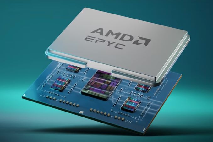
As part of AMD's Q1'2024 earnings announcement this week, the company is offering a brief status update on some of their future products set to launch later this year. Most important among these is an update on their Zen 5 CPU architecture, which is expected to launch for both client and server products later this year.
Highlighting their progress so far, AMD is confirming that EPYC "Turin" processors have begun sampling, and that these early runs of AMD's next-gen datacenter chips are meeting the company's expectations.
"Looking ahead, we are very excited about our next-gen Turin family of EPYC processors featuring our Zen 5 core," said Lisa Su, chief executive officer of AMD, at the conference call with analysts and investors (via SeekingAlpha). "We are widely sampling Turin, and the silicon is looking great. In the cloud, the significant performance and efficiency increases of Turin position us well to capture an even larger share of both first and third-party workloads."
Overall, it looks like AMD is on-track to solidify its position, and perhaps even increase its datacenter market share with its EPYC Turin processors. According to AMD, the company's server partners are developing a 30% larger number of designs for Turin than they did Genoa. This underscores how AMD's partners are preparing for even more market share growth on the back of AMD's ongoing success, not to mention the improved performance and power efficiency that the Zen 5 architecture should offer.
"In addition, there are 30% more Turin platforms in development from our server partners, compared to 4th Generation EPYC platforms, increasing our enterprise and with new solutions optimized for additional workloads," Su said. "Turin remains on track to launch later this year."
AMD's EPYC 'Turin' processors will be drop-in compatible with existing SP5 platforms (i.e., will come in an LGA 6096 package), which will facilitate its faster ramp and adoption of the platform both by cloud giants and server makers. In addition, AMD's next-generation EPYC CPUs are expected to feature more than 96 cores and a more versatile memory subsystem.
CPUs

A few years back, the Japanese government's New Energy and Industrial Technology Development Organization (NEDO ) allocated funding for the development of green datacenter technologies. With the aim to obtain up to 40% savings in overall power consumption, several Japanese companies have been developing an optical interface for their enterprise SSDs. And at this year's FMS, Kioxia had their optical interface on display.

For this demonstration, Kioxia took its existing CM7 enterprise SSD and created an optical interface for it. A PCIe card with on-board optics developed by Kyocera is installed in the server slot. An optical interface allows data transfer over long distances (it was 40m in the demo, but Kioxia promises lengths of up to 100m for the cable in the future). This allows the storage to be kept in a separate room with minimal cooling requirements compared to the rack with the CPUs and GPUs. Disaggregation of different server components will become an option as very high throughput interfaces such as PCIe 7.0 (with 128 GT/s rates) become available.

The demonstration of the optical SSD showed a slight loss in IOPS performance, but a significant advantage in the latency metric over the shipping enterprise SSD behind a copper network link. Obviously, there are advantages in wiring requirements and signal integrity maintenance with optical links.
Being a proof-of-concept demonstration, we do see the requirement for an industry-standard approach if this were to gain adoption among different datacenter vendors. The PCI-SIG optical workgroup will need to get its act together soon to create a standards-based approach to this problem.
Storage
A few years back, the Japanese government's New Energy and Industrial Technology Development Organization (NEDO ) allocated funding for the development of green datacenter technologies. With the aim to obtain up to 40% savings in overall power consumption, several Japanese companies have been developing an optical interface for their enterprise SSDs. And at this year's FMS, Kioxia had their optical interface on display.
For this demonstration, Kioxia took its existing CM7 enterprise SSD and created an optical interface for it. A PCIe card with on-board optics developed by Kyocera is installed in the server slot. An optical interface allows data transfer over long distances (it was 40m in the demo, but Kioxia promises lengths of up to 100m for the cable in the future). This allows the storage to be kept in a separate room with minimal cooling requirements compared to the rack with the CPUs and GPUs. Disaggregation of different server components will become an option as very high throughput interfaces such as PCIe 7.0 (with 128 GT/s rates) become available.
The demonstration of the optical SSD showed a slight loss in IOPS performance, but a significant advantage in the latency metric over the shipping enterprise SSD behind a copper network link. Obviously, there are advantages in wiring requirements and signal integrity maintenance with optical links.
Being a proof-of-concept demonstration, we do see the requirement for an industry-standard approach if this were to gain adoption among different datacenter vendors. The PCI-SIG optical workgroup will need to get its act together soon to create a standards-based approach to this problem.
Storage
As part of AMD's Q1'2024 earnings announcement this week, the company is offering a brief status update on some of their future products set to launch later this year. Most important among these is an update on their Zen 5 CPU architecture, which is expected to launch for both client and server products later this year.
Highlighting their progress so far, AMD is confirming that EPYC "Turin" processors have begun sampling, and that these early runs of AMD's next-gen datacenter chips are meeting the company's expectations.
"Looking ahead, we are very excited about our next-gen Turin family of EPYC processors featuring our Zen 5 core," said Lisa Su, chief executive officer of AMD, at the conference call with analysts and investors (via SeekingAlpha). "We are widely sampling Turin, and the silicon is looking great. In the cloud, the significant performance and efficiency increases of Turin position us well to capture an even larger share of both first and third-party workloads."
Overall, it looks like AMD is on-track to solidify its position, and perhaps even increase its datacenter market share with its EPYC Turin processors. According to AMD, the company's server partners are developing a 30% larger number of designs for Turin than they did Genoa. This underscores how AMD's partners are preparing for even more market share growth on the back of AMD's ongoing success, not to mention the improved performance and power efficiency that the Zen 5 architecture should offer.
"In addition, there are 30% more Turin platforms in development from our server partners, compared to 4th Generation EPYC platforms, increasing our enterprise and with new solutions optimized for additional workloads," Su said. "Turin remains on track to launch later this year."
AMD's EPYC 'Turin' processors will be drop-in compatible with existing SP5 platforms (i.e., will come in an LGA 6096 package), which will facilitate its faster ramp and adoption of the platform both by cloud giants and server makers. In addition, AMD's next-generation EPYC CPUs are expected to feature more than 96 cores and a more versatile memory subsystem.
CPUs
A few years back, the Japanese government's New Energy and Industrial Technology Development Organization (NEDO ) allocated funding for the development of green datacenter technologies. With the aim to obtain up to 40% savings in overall power consumption, several Japanese companies have been developing an optical interface for their enterprise SSDs. And at this year's FMS, Kioxia had their optical interface on display.
For this demonstration, Kioxia took its existing CM7 enterprise SSD and created an optical interface for it. A PCIe card with on-board optics developed by Kyocera is installed in the server slot. An optical interface allows data transfer over long distances (it was 40m in the demo, but Kioxia promises lengths of up to 100m for the cable in the future). This allows the storage to be kept in a separate room with minimal cooling requirements compared to the rack with the CPUs and GPUs. Disaggregation of different server components will become an option as very high throughput interfaces such as PCIe 7.0 (with 128 GT/s rates) become available.
The demonstration of the optical SSD showed a slight loss in IOPS performance, but a significant advantage in the latency metric over the shipping enterprise SSD behind a copper network link. Obviously, there are advantages in wiring requirements and signal integrity maintenance with optical links.
Being a proof-of-concept demonstration, we do see the requirement for an industry-standard approach if this were to gain adoption among different datacenter vendors. The PCI-SIG optical workgroup will need to get its act together soon to create a standards-based approach to this problem.
Storage
It is with great sadness that I find myself penning the hardest news post I’ve ever needed to write here at AnandTech. After over 27 years of covering the wide – and wild – world of computing hardware, today is AnandTech’s final day of publication.
For better or worse, we’ve reached the end of a long journey – one that started with a review of an AMD processor, and has ended with the review of an AMD processor. It’s fittingly poetic, but it is also a testament to the fact that we’ve spent the last 27 years doing what we love, covering the chips that are the lifeblood of the computing industry.
A lot of things have changed in the last quarter-century – in 1997 NVIDIA had yet to even coin the term “GPU” – and we’ve been fortunate to watch the world of hardware continue to evolve over the time period. We’ve gone from boxy desktop computers and laptops that today we’d charitably classify as portable desktops, to pocket computers where even the cheapest budget device puts the fastest PC of 1997 to shame.
The years have also brought some monumental changes to the world of publishing. AnandTech was hardly the first hardware enthusiast website, nor will we be the last. But we were fortunate to thrive in the past couple of decades, when so many of our peers did not, thanks to a combination of hard work, strategic investments in people and products, even more hard work, and the support of our many friends, colleagues, and readers.
Still, few things last forever, and the market for written tech journalism is not what it once was – nor will it ever be again. So, the time has come for AnandTech to wrap up its work, and let the next generation of tech journalists take their place within the zeitgeist.
It has been my immense privilege to write for AnandTech for the past 19 years – and to manage it as its editor-in-chief for the past decade. And while I carry more than a bit of remorse in being AnandTech’s final boss, I can at least take pride in everything we’ve accomplished over the years, whether it’s lauding some legendary products, writing technology primers that still remain relevant today, or watching new stars rise in expected places. There is still more that I had wanted AnandTech to do, but after 21,500 articles, this was a good start.
And while the AnandTech staff is riding off into the sunset, I am happy to report that the site itself won’t be going anywhere for a while. Our publisher, Future PLC, will be keeping the AnandTech website and its many articles live indefinitely. So that all of the content we’ve created over the years remains accessible and citable. Even without new articles to add to the collection, I expect that many of the things we’ve written over the past couple of decades will remain relevant for years to come – and remain accessible just as long.
The AnandTech Forums will also continue to be operated by Future’s community team and our dedicated troop of moderators. With forum threads going back to 1999 (and some active members just as long), the forums have a history almost as long and as storied as AnandTech itself (wounded monitor children, anyone?). So even when AnandTech is no longer publishing articles, we’ll still have a place for everyone to talk about the latest in technology – and have those discussions last longer than 48 hours.
Finally, for everyone who still needs their technical writing fix, our formidable opposition of the last 27 years and fellow Future brand, Tom’s Hardware, is continuing to cover the world of technology. There are a couple of familiar AnandTech faces already over there providing their accumulated expertise, and the site will continue doing its best to provide a written take on technology news.
As I look back on everything AnandTech has accomplished over the past 27 years, there are more than a few people, groups, and companies that I would like to thank on behalf of both myself and AnandTech as a whole.
First and foremost, I cannot thank enough all the editors who have worked for AnandTech over the years. T... Site Updates

Lorem Ipsum is simply dummy text of the printing and typesetting industry. Lorem Ipsum has been the industry's.
As part of AMD's Q1'2024 earnings announcement this week, the company is offering a brief status update on some of their future products set to launch later this year. Most important among these is an update on their Zen 5 CPU architecture, which is expected to launch for both client and server products later this year.
Highlighting their progress so far, AMD is confirming that EPYC "Turin" processors have begun sampling, and that these early runs of AMD's next-gen datacenter chips are meeting the company's expectations.
"Looking ahead, we are very excited about our next-gen Turin family of EPYC processors featuring our Zen 5 core," said Lisa Su, chief executive officer of AMD, at the conference call with analysts and investors (via SeekingAlpha). "We are widely sampling Turin, and the silicon is looking great. In the cloud, the significant performance and efficiency increases of Turin position us well to capture an even larger share of both first and third-party workloads."
Overall, it looks like AMD is on-track to solidify its position, and perhaps even increase its datacenter market share with its EPYC Turin processors. According to AMD, the company's server partners are developing a 30% larger number of designs for Turin than they did Genoa. This underscores how AMD's partners are preparing for even more market share growth on the back of AMD's ongoing success, not to mention the improved performance and power efficiency that the Zen 5 architecture should offer.
"In addition, there are 30% more Turin platforms in development from our server partners, compared to 4th Generation EPYC platforms, increasing our enterprise and with new solutions optimized for additional workloads," Su said. "Turin remains on track to launch later this year."
AMD's EPYC 'Turin' processors will be drop-in compatible with existing SP5 platforms (i.e., will come in an LGA 6096 package), which will facilitate its faster ramp and adoption of the platform both by cloud giants and server makers. In addition, AMD's next-generation EPYC CPUs are expected to feature more than 96 cores and a more versatile memory subsystem.
CPUs
A few years back, the Japanese government's New Energy and Industrial Technology Development Organization (NEDO ) allocated funding for the development of green datacenter technologies. With the aim to obtain up to 40% savings in overall power consumption, several Japanese companies have been developing an optical interface for their enterprise SSDs. And at this year's FMS, Kioxia had their optical interface on display.
For this demonstration, Kioxia took its existing CM7 enterprise SSD and created an optical interface for it. A PCIe card with on-board optics developed by Kyocera is installed in the server slot. An optical interface allows data transfer over long distances (it was 40m in the demo, but Kioxia promises lengths of up to 100m for the cable in the future). This allows the storage to be kept in a separate room with minimal cooling requirements compared to the rack with the CPUs and GPUs. Disaggregation of different server components will become an option as very high throughput interfaces such as PCIe 7.0 (with 128 GT/s rates) become available.
The demonstration of the optical SSD showed a slight loss in IOPS performance, but a significant advantage in the latency metric over the shipping enterprise SSD behind a copper network link. Obviously, there are advantages in wiring requirements and signal integrity maintenance with optical links.
Being a proof-of-concept demonstration, we do see the requirement for an industry-standard approach if this were to gain adoption among different datacenter vendors. The PCI-SIG optical workgroup will need to get its act together soon to create a standards-based approach to this problem.
Storage
A few years back, the Japanese government's New Energy and Industrial Technology Development Organization (NEDO ) allocated funding for the development of green datacenter technologies. With the aim to obtain up to 40% savings in overall power consumption, several Japanese companies have been developing an optical interface for their enterprise SSDs. And at this year's FMS, Kioxia had their optical interface on display.
For this demonstration, Kioxia took its existing CM7 enterprise SSD and created an optical interface for it. A PCIe card with on-board optics developed by Kyocera is installed in the server slot. An optical interface allows data transfer over long distances (it was 40m in the demo, but Kioxia promises lengths of up to 100m for the cable in the future). This allows the storage to be kept in a separate room with minimal cooling requirements compared to the rack with the CPUs and GPUs. Disaggregation of different server components will become an option as very high throughput interfaces such as PCIe 7.0 (with 128 GT/s rates) become available.
The demonstration of the optical SSD showed a slight loss in IOPS performance, but a significant advantage in the latency metric over the shipping enterprise SSD behind a copper network link. Obviously, there are advantages in wiring requirements and signal integrity maintenance with optical links.
Being a proof-of-concept demonstration, we do see the requirement for an industry-standard approach if this were to gain adoption among different datacenter vendors. The PCI-SIG optical workgroup will need to get its act together soon to create a standards-based approach to this problem.
Storage
 not available on other off-the-shelf controllers – or on any previous Western Digital controllers. </p>
<p>The Ultrastar DC SN861 SSD offers sequential read speeds up to 13.7 GB/s as well as sequential write speeds up to 7.5 GB/s. As for random performance, it boasts with an up to 3.3 million random 4K read IOPS and up to 0.8 million random 4K write IOPS. The drives are available in capacities between 1.6 TB and 7.68 TB with one or three drive writes per day (DWPD) over five years rating as well as in U.2 and E1.S form-factors. </p>
<p>While the two form factors of the SN861 share a similar technical design, Western Digital has tailored each version for distinct workloads: the E1.S supports FDP and performance enhancements specifically for cloud environments. By contrast, the U.2 model is geared towards high-performance enterprise tasks and emerging applications like AI.</p>
<p>Without any doubts, Western Digital's Ultrastar DC SN861 is a feature-rich high-performance enterprise-grade SSD. It has another distinctive feature: a 5W idle power consumption, which is rather low by the standards of enterprise-grade drives (e.g., it is 1W lower compared to the SN840). While the difference with predecessors may be just 1W, hyperscalers deploy thousands of drives and for their TCO every watt counts.</p>
<p>Western Digital's Ultrastar DC SN861 SSDs are now available for purchase to select customers (such as Meta) and to interested parties. Prices are unknown, but they will depend on such factors as volumes.</p>
<p>Sources: <a href="https://www.fadu.io/en/fc5161-gen5/">Fadu</a>, <a href="https://www.storagereview.com/review/western-digital-sn861-gen5-ssd-versatile-solutions-for-modern-hyperscale-and-enterprise-needs">Storage Review</a></p>
</p> Storage)
 not available on other off-the-shelf controllers – or on any previous Western Digital controllers. </p>
<p>The Ultrastar DC SN861 SSD offers sequential read speeds up to 13.7 GB/s as well as sequential write speeds up to 7.5 GB/s. As for random performance, it boasts with an up to 3.3 million random 4K read IOPS and up to 0.8 million random 4K write IOPS. The drives are available in capacities between 1.6 TB and 7.68 TB with one or three drive writes per day (DWPD) over five years rating as well as in U.2 and E1.S form-factors. </p>
<p>While the two form factors of the SN861 share a similar technical design, Western Digital has tailored each version for distinct workloads: the E1.S supports FDP and performance enhancements specifically for cloud environments. By contrast, the U.2 model is geared towards high-performance enterprise tasks and emerging applications like AI.</p>
<p>Without any doubts, Western Digital's Ultrastar DC SN861 is a feature-rich high-performance enterprise-grade SSD. It has another distinctive feature: a 5W idle power consumption, which is rather low by the standards of enterprise-grade drives (e.g., it is 1W lower compared to the SN840). While the difference with predecessors may be just 1W, hyperscalers deploy thousands of drives and for their TCO every watt counts.</p>
<p>Western Digital's Ultrastar DC SN861 SSDs are now available for purchase to select customers (such as Meta) and to interested parties. Prices are unknown, but they will depend on such factors as volumes.</p>
<p>Sources: <a href="https://www.fadu.io/en/fc5161-gen5/">Fadu</a>, <a href="https://www.storagereview.com/review/western-digital-sn861-gen5-ssd-versatile-solutions-for-modern-hyperscale-and-enterprise-needs">Storage Review</a></p>
</p> Storage | https://compbuddey.blogspot.com/2025/03/fadus-fc5161-ssd-controller-breaks_76.html)
 not available on other off-the-shelf controllers – or on any previous Western Digital controllers. </p>
<p>The Ultrastar DC SN861 SSD offers sequential read speeds up to 13.7 GB/s as well as sequential write speeds up to 7.5 GB/s. As for random performance, it boasts with an up to 3.3 million random 4K read IOPS and up to 0.8 million random 4K write IOPS. The drives are available in capacities between 1.6 TB and 7.68 TB with one or three drive writes per day (DWPD) over five years rating as well as in U.2 and E1.S form-factors. </p>
<p>While the two form factors of the SN861 share a similar technical design, Western Digital has tailored each version for distinct workloads: the E1.S supports FDP and performance enhancements specifically for cloud environments. By contrast, the U.2 model is geared towards high-performance enterprise tasks and emerging applications like AI.</p>
<p>Without any doubts, Western Digital's Ultrastar DC SN861 is a feature-rich high-performance enterprise-grade SSD. It has another distinctive feature: a 5W idle power consumption, which is rather low by the standards of enterprise-grade drives (e.g., it is 1W lower compared to the SN840). While the difference with predecessors may be just 1W, hyperscalers deploy thousands of drives and for their TCO every watt counts.</p>
<p>Western Digital's Ultrastar DC SN861 SSDs are now available for purchase to select customers (such as Meta) and to interested parties. Prices are unknown, but they will depend on such factors as volumes.</p>
<p>Sources: <a href="https://www.fadu.io/en/fc5161-gen5/">Fadu</a>, <a href="https://www.storagereview.com/review/western-digital-sn861-gen5-ssd-versatile-solutions-for-modern-hyperscale-and-enterprise-needs">Storage Review</a></p>
</p> Storage&body=https://compbuddey.blogspot.com/2025/03/fadus-fc5161-ssd-controller-breaks_76.html)
0 Comments