

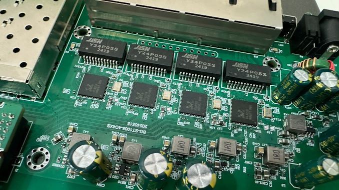
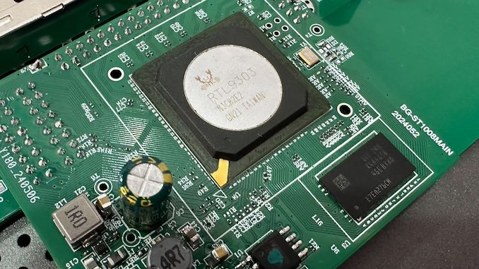
When Western Digital introduced its Ultrastar DC SN861 SSDs earlier this year, the company did not disclose which controller it used for these drives, which made many observers presume that WD was using an in-house controller. But a recent teardown of the drive shows that is not the case; instead, the company is using a controller from Fadu, a South Korean company founded in 2015 that specializes on enterprise-grade turnkey SSD solutions.
The Western Digital Ultrastar DC SN861 SSD is aimed at performance-hungry hyperscale datacenters and enterprise customers which are adopting PCIe Gen5 storage devices these days. And, as uncovered in photos from a recent Storage Review article, the drive is based on Fadu's FC5161 NVMe 2.0-compliant controller. The FC5161 utilizes 16 NAND channels supporting an ONFi 5.0 2400 MT/s interface, and features a combination of enterprise-grade capabilities (OCP Cloud Spec 2.0, SR-IOV, up to 512 name spaces for ZNS support, flexible data placement, NVMe-MI 1.2, advanced security, telemetry, power loss protection) not available on other off-the-shelf controllers – or on any previous Western Digital controllers.
The Ultrastar DC SN861 SSD offers sequential read speeds up to 13.7 GB/s as well as sequential write speeds up to 7.5 GB/s. As for random performance, it boasts with an up to 3.3 million random 4K read IOPS and up to 0.8 million random 4K write IOPS. The drives are available in capacities between 1.6 TB and 7.68 TB with one or three drive writes per day (DWPD) over five years rating as well as in U.2 and E1.S form-factors.
While the two form factors of the SN861 share a similar technical design, Western Digital has tailored each version for distinct workloads: the E1.S supports FDP and performance enhancements specifically for cloud environments. By contrast, the U.2 model is geared towards high-performance enterprise tasks and emerging applications like AI.
Without any doubts, Western Digital's Ultrastar DC SN861 is a feature-rich high-performance enterprise-grade SSD. It has another distinctive feature: a 5W idle power consumption, which is rather low by the standards of enterprise-grade drives (e.g., it is 1W lower compared to the SN840). While the difference with predecessors may be just 1W, hyperscalers deploy thousands of drives and for their TCO every watt counts.
Western Digital's Ultrastar DC SN861 SSDs are now available for purchase to select customers (such as Meta) and to interested parties. Prices are unknown, but they will depend on such factors as volumes.
Sources: Fadu, Storage Review
Storage

Kioxia's booth at FMS 2024 was a busy one with multiple technology demonstrations keeping visitors occupied. A walk-through of the BiCS 8 manufacturing process was the first to grab my attention. Kioxia and Western Digital announced the sampling of BiCS 8 in March 2023. We had touched briefly upon its CMOS Bonded Array (CBA) scheme in our coverage of Kioxial's 2Tb QLC NAND device and coverage of Western Digital's 128 TB QLC enterprise SSD proof-of-concept demonstration. At Kioxia's booth, we got more insights.

Traditionally, fabrication of flash chips involved placement of the associate logic circuitry (CMOS process) around the periphery of the flash array. The process then moved on to putting the CMOS under the cell array, but the wafer development process was serialized with the CMOS logic getting fabricated first followed by the cell array on top. However, this has some challenges because the cell array requires a high-temperature processing step to ensure higher reliability that can be detrimental to the health of the CMOS logic. Thanks to recent advancements in wafer bonding techniques, the new CBA process allows the CMOS wafer and cell array wafer to be processed independently in parallel and then pieced together, as shown in the models above.

The BiCS 8 3D NAND incorporates 218 layers, compared to 112 layers in BiCS 5 and 162 layers in BiCS 6. The company decided to skip over BiCS 7 (or, rather, it was probably a short-lived generation meant as an internal test vehicle). The generation retains the four-plane charge trap structure of BiCS 6. In its TLC avatar, it is available as a 1 Tbit device. The QLC version is available in two capacities - 1 Tbit and 2 Tbit.
Kioxia also noted that while the number of layers (218) doesn't compare favorably with the latest layer counts from the competition, its lateral scaling / cell shrinkage has enabled it to be competitive in terms of bit density as well as operating speeds (3200 MT/s). For reference, the latest shipping NAND from Micron - the G9 - has 276 layers with a bit density in TLC mode of 21 Gbit/mm2, and operates at up to 3600 MT/s. However, its 232L NAND operates only up to 2400 MT/s and has a bit density of 14.6 Gbit/mm2.
It must be noted that the CBA hybrid bonding process has advantages over the current processes used by other vendors - including Micron's CMOS under array (CuA) and SK hynix's 4D PUC (periphery-under-chip) developed in the late 2010s. It is expected that other NAND vendors will also move eventually to some variant of the hybrid bonding scheme used by Kioxia.
Storage
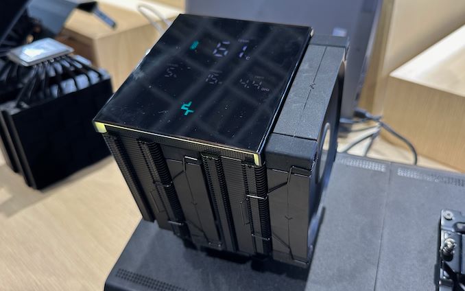
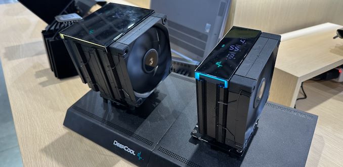
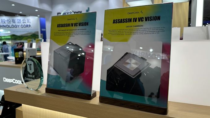
While the market for high-end CPU coolers has decidedly shifted towards closed-loop all-in-one liquid coolers over the last several years, air cooling remains alive and well. Even at the high-end, there are still further improvements and innovations being made, such as DeepCool's vapor chamber-based tower cooler, which was demonstrated at Computex.
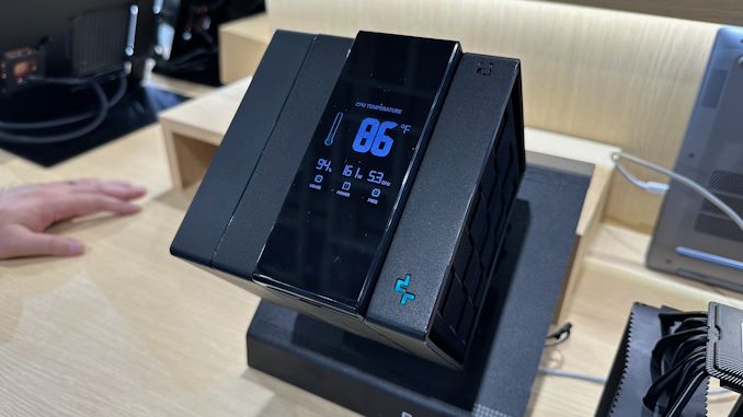
Named the Assassin IV VC Vision, DeepCool's design is an advanced concept vehicle that equips a tower cooled with both a vapor chamber in the base as well as has an LCD pad on top for extra flourish. The vapor chamber is said to increase the cooling capacity by 20W, adding a bit more of an edge to an already very powerful tower cooler design.
While we expect this one to come to market eventually, don't be surprised if both vapor chamber and the screen to land on other products together or separately. For example, the massive DeepCool Assassin IV VC Vision has a more compact brother that has a screen and a vapor chamber.
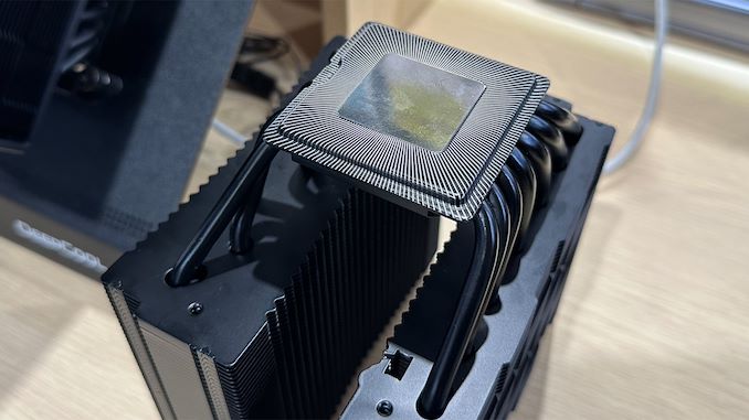
The unit builds on top of the already monstrous DeepCool Assassin IV that comes with seven 0.6-mm heat pipes and can mount up to three 120/140mm fans, depending on installation (one is magnetically attached). With a weight of 1.575 kilograms – almost entirely copper and aluminum – this one is already good enough to cool down even the highest-performing CPUs.
DeepCool is currently trying to figure out recommended pricing for its Assassin IV VC Vision cooler, but the original Assassin IV costs $99.99, so expect the unit with a vapor chamber and a screen to build on top of that.
Kioxia's booth at FMS 2024 was a busy one with multiple technology demonstrations keeping visitors occupied. A walk-through of the BiCS 8 manufacturing process was the first to grab my attention. Kioxia and Western Digital announced the sampling of BiCS 8 in March 2023. We had touched briefly upon its CMOS Bonded Array (CBA) scheme in our coverage of Kioxial's 2Tb QLC NAND device and coverage of Western Digital's 128 TB QLC enterprise SSD proof-of-concept demonstration. At Kioxia's booth, we got more insights.
Traditionally, fabrication of flash chips involved placement of the associate logic circuitry (CMOS process) around the periphery of the flash array. The process then moved on to putting the CMOS under the cell array, but the wafer development process was serialized with the CMOS logic getting fabricated first followed by the cell array on top. However, this has some challenges because the cell array requires a high-temperature processing step to ensure higher reliability that can be detrimental to the health of the CMOS logic. Thanks to recent advancements in wafer bonding techniques, the new CBA process allows the CMOS wafer and cell array wafer to be processed independently in parallel and then pieced together, as shown in the models above.
The BiCS 8 3D NAND incorporates 218 layers, compared to 112 layers in BiCS 5 and 162 layers in BiCS 6. The company decided to skip over BiCS 7 (or, rather, it was probably a short-lived generation meant as an internal test vehicle). The generation retains the four-plane charge trap structure of BiCS 6. In its TLC avatar, it is available as a 1 Tbit device. The QLC version is available in two capacities - 1 Tbit and 2 Tbit.
Kioxia also noted that while the number of layers (218) doesn't compare favorably with the latest layer counts from the competition, its lateral scaling / cell shrinkage has enabled it to be competitive in terms of bit density as well as operating speeds (3200 MT/s). For reference, the latest shipping NAND from Micron - the G9 - has 276 layers with a bit density in TLC mode of 21 Gbit/mm2, and operates at up to 3600 MT/s. However, its 232L NAND operates only up to 2400 MT/s and has a bit density of 14.6 Gbit/mm2.
It must be noted that the CBA hybrid bonding process has advantages over the current processes used by other vendors - including Micron's CMOS under array (CuA) and SK hynix's 4D PUC (periphery-under-chip) developed in the late 2010s. It is expected that other NAND vendors will also move eventually to some variant of the hybrid bonding scheme used by Kioxia.
Storage
While the market for high-end CPU coolers has decidedly shifted towards closed-loop all-in-one liquid coolers over the last several years, air cooling remains alive and well. Even at the high-end, there are still further improvements and innovations being made, such as DeepCool's vapor chamber-based tower cooler, which was demonstrated at Computex.
Named the Assassin IV VC Vision, DeepCool's design is an advanced concept vehicle that equips a tower cooled with both a vapor chamber in the base as well as has an LCD pad on top for extra flourish. The vapor chamber is said to increase the cooling capacity by 20W, adding a bit more of an edge to an already very powerful tower cooler design.
While we expect this one to come to market eventually, don't be surprised if both vapor chamber and the screen to land on other products together or separately. For example, the massive DeepCool Assassin IV VC Vision has a more compact brother that has a screen and a vapor chamber.
The unit builds on top of the already monstrous DeepCool Assassin IV that comes with seven 0.6-mm heat pipes and can mount up to three 120/140mm fans, depending on installation (one is magnetically attached). With a weight of 1.575 kilograms – almost entirely copper and aluminum – this one is already good enough to cool down even the highest-performing CPUs.
DeepCool is currently trying to figure out recommended pricing for its Assassin IV VC Vision cooler, but the original Assassin IV costs $99.99, so expect the unit with a vapor chamber and a screen to build on top of that.


Under the CHIPS & Science Act, the U.S. government provided tens of billions of dollars in grants and loans to the world's leading maker of chips, such as Intel, Samsung, and TSMC, which will significantly expand the country's semiconductor production industry in the coming years. However, most chips are typically tested, assembled, and packaged in Asia, which has left the American supply chain incomplete. Addressing this last gap in the government's domestic chip production plans, these past couple of weeks the U.S. government signed memorandums of understanding worth about $1.5 billion with Amkor and SK hynix to support their efforts to build chip packaging facilities in the U.S.
Amkor plans to build a $2 billion advanced packaging facility near Peoria, Arizona, to test and assemble chips produced by TSMC at its Fab 21 near Phoenix, Arizona. The company signed a MOU that offers $400 million in direct funding and access to $200 million in loans under the CHIPS & Science Act. In addition, the company plans to take advantage of a 25% investment tax credit on eligible capital expenditures.
Set to be strategically positioned near TSMC's upcoming Fab 21 complex in Arizona, Amkor's Peoria facility will occupy 55 acres and, when fully completed, will feature over 500,000 square feet (46,451 square meters) of cleanroom space, more than twice the size of Amkor's advanced packaging site in Vietnam. Although the company has not disclosed the exact capacity or the specific technologies the facility will support, it is expected to cater to a wide range of industries, including automotive, high-performance computing, and mobile technologies. This suggests the new plant will offer diverse packaging solutions, including traditional, 2.5D, and 3D technologies.
Amkor has collaborated extensively with Apple on the vision and initial setup of the Peoria facility, as Apple is slated to be the facility's first and largest customer, marking a significant commitment from the tech giant. This partnership highlights the importance of the new facility in reinforcing the U.S. semiconductor supply chain and positioning Amkor as a key partner for companies relying on TSMC's manufacturing capabilities. The project is expected to generate around 2,000 jobs and is scheduled to begin operations in 2027.
This week SK hynix also signed a preliminary agreement with the U.S. government to receive up to $450 million in direct funding and $500 million in loans to build an advanced memory packaging facility in West Lafayette, Indiana.
The proposed facility is scheduled to begin operations in 2028, which means that it will assemble HBM4 or HBM4E memory. Meanwhile, DRAM devices for high bandwidth memory (HBM) stacks will still be produced in South Korea. Nonetheless, packing finished HBM4/HBM4E in the U.S. and possibly integrating these memory modules with high-end processors is a big deal.
In addition to building its packaging plant, SK hynix plans to collaborate with Purdue University and other local research institutions to advance semiconductor technology and packaging innovations. This partnership is intended to bolster research and development in the region, positioning the facility as a hub for AI technology and skilled employment.
Semiconductors
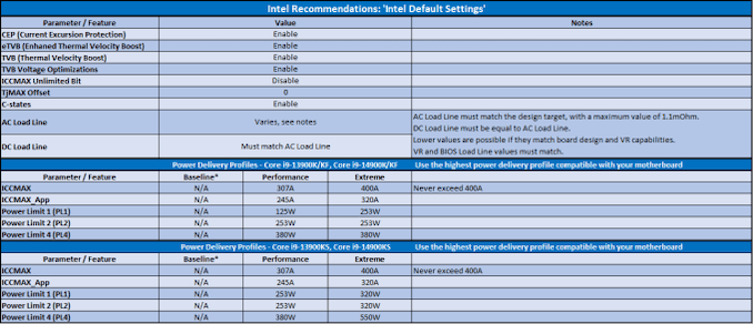
Further to our last piece which we detailed Intel's issue to motherboard vendors to follow with stock power settings for Intel's 14th and 13th Gen Core series processors, Intel has now issued a follow-up statement to this. Over the last week or so, motherboard vendors quickly released firmware updates with a new profile called 'Intel Baseline', which motherboard vendors assumed would address the instability issues.
As it turns out, Intel doesn't seem to accept this as technically, these Intel Baseline profiles are not to be confused with Intel's default specifications. This means that Intel's Baseline profiles seemingly give the impression that they are operating at default settings, hence the terminology 'baseline' used, but this still opens motherboard vendors to use their interpretations of MCE or Multi-Core Enhancement.
To clarify things for consumers, Intel has sent us the following statement:
Several motherboard manufacturers have released BIOS profiles labeled ‘Intel Baseline Profile’. However, these BIOS profiles are not the same as the 'Intel Default Settings' recommendations that Intel has recently shared with its partners regarding the instability issues reported on 13th and 14th gen K SKU processors.
These ‘Intel Baseline Profile’ BIOS settings appear to be based on power delivery guidance previously provided by Intel to manufacturers describing the various power delivery options for 13th and 14th Generation K SKU processors based on motherboard capabilities.
Intel is not recommending motherboard manufacturers to use ‘baseline’ power delivery settings on boards capable of higher values.
Intel’s recommended ‘Intel Default Settings’ are a combination of thermal and power delivery features along with a selection of possible power delivery profiles based on motherboard capabilities.
Intel recommends customers to implement the highest power delivery profile compatible with each individual motherboard design as noted in the table below:
Click to Enlarge Intel's Default Settings
What Intel's statement is effectively saying to consumers, is that users shouldn't be using the Baseline Power Delivery profiles which are offered by motherboard vendors through a plethora of firmware updates. Instead, Intel is recommending users opt for Intel Default Settings, which follows what the specific processor is rated for by Intel out of the box to achieve the clock speeds advertised, without users having to worry about firmware 'over' optimization which can cause instability as there have been many reports of happening.
Not only this, but the Intel Default settings offer a combination of thermal specifications and power capabilities, including voltage and frequency curve settings that apply to the capability of the motherboard used, and the power delivery equipped on the motherboard. At least for the most part, Intel is recommending users with 14th and 13th-Gen Core series K, KF, and KS SKUs that they do not recommend users opt in using the Baseline profiles offered by motherboard vendors.
Digesting the contrast between the two statements, the key differential is that Intel's priority is reducing the current going through the processor, which for both the 14th and 13th Gen Core series processors is a maximum of 400 A, even when using the Extreme profile. We know those motherboard vendors on their Z790 and Z690 motherboards opt for an unrestricted power profile, which is essentially 'unlimited' power and current to maximize performance at the cost of power consumption and heat, which does exacerbate problems and can lead to frequent bouts of instability, especially on high-intensity workloads.
Another variable Intel is recommending is that the AC Load Line must match the design target of the processor, with a maximum value of 1.1 mOhm, and that the DC Load Line must be ... CPUs
Kioxia's booth at FMS 2024 was a busy one with multiple technology demonstrations keeping visitors occupied. A walk-through of the BiCS 8 manufacturing process was the first to grab my attention. Kioxia and Western Digital announced the sampling of BiCS 8 in March 2023. We had touched briefly upon its CMOS Bonded Array (CBA) scheme in our coverage of Kioxial's 2Tb QLC NAND device and coverage of Western Digital's 128 TB QLC enterprise SSD proof-of-concept demonstration. At Kioxia's booth, we got more insights.
Traditionally, fabrication of flash chips involved placement of the associate logic circuitry (CMOS process) around the periphery of the flash array. The process then moved on to putting the CMOS under the cell array, but the wafer development process was serialized with the CMOS logic getting fabricated first followed by the cell array on top. However, this has some challenges because the cell array requires a high-temperature processing step to ensure higher reliability that can be detrimental to the health of the CMOS logic. Thanks to recent advancements in wafer bonding techniques, the new CBA process allows the CMOS wafer and cell array wafer to be processed independently in parallel and then pieced together, as shown in the models above.
The BiCS 8 3D NAND incorporates 218 layers, compared to 112 layers in BiCS 5 and 162 layers in BiCS 6. The company decided to skip over BiCS 7 (or, rather, it was probably a short-lived generation meant as an internal test vehicle). The generation retains the four-plane charge trap structure of BiCS 6. In its TLC avatar, it is available as a 1 Tbit device. The QLC version is available in two capacities - 1 Tbit and 2 Tbit.
Kioxia also noted that while the number of layers (218) doesn't compare favorably with the latest layer counts from the competition, its lateral scaling / cell shrinkage has enabled it to be competitive in terms of bit density as well as operating speeds (3200 MT/s). For reference, the latest shipping NAND from Micron - the G9 - has 276 layers with a bit density in TLC mode of 21 Gbit/mm2, and operates at up to 3600 MT/s. However, its 232L NAND operates only up to 2400 MT/s and has a bit density of 14.6 Gbit/mm2.
It must be noted that the CBA hybrid bonding process has advantages over the current processes used by other vendors - including Micron's CMOS under array (CuA) and SK hynix's 4D PUC (periphery-under-chip) developed in the late 2010s. It is expected that other NAND vendors will also move eventually to some variant of the hybrid bonding scheme used by Kioxia.
Storage
Lorem Ipsum is simply dummy text of the printing and typesetting industry. Lorem Ipsum has been the industry's.
Kioxia's booth at FMS 2024 was a busy one with multiple technology demonstrations keeping visitors occupied. A walk-through of the BiCS 8 manufacturing process was the first to grab my attention. Kioxia and Western Digital announced the sampling of BiCS 8 in March 2023. We had touched briefly upon its CMOS Bonded Array (CBA) scheme in our coverage of Kioxial's 2Tb QLC NAND device and coverage of Western Digital's 128 TB QLC enterprise SSD proof-of-concept demonstration. At Kioxia's booth, we got more insights.
Traditionally, fabrication of flash chips involved placement of the associate logic circuitry (CMOS process) around the periphery of the flash array. The process then moved on to putting the CMOS under the cell array, but the wafer development process was serialized with the CMOS logic getting fabricated first followed by the cell array on top. However, this has some challenges because the cell array requires a high-temperature processing step to ensure higher reliability that can be detrimental to the health of the CMOS logic. Thanks to recent advancements in wafer bonding techniques, the new CBA process allows the CMOS wafer and cell array wafer to be processed independently in parallel and then pieced together, as shown in the models above.
The BiCS 8 3D NAND incorporates 218 layers, compared to 112 layers in BiCS 5 and 162 layers in BiCS 6. The company decided to skip over BiCS 7 (or, rather, it was probably a short-lived generation meant as an internal test vehicle). The generation retains the four-plane charge trap structure of BiCS 6. In its TLC avatar, it is available as a 1 Tbit device. The QLC version is available in two capacities - 1 Tbit and 2 Tbit.
Kioxia also noted that while the number of layers (218) doesn't compare favorably with the latest layer counts from the competition, its lateral scaling / cell shrinkage has enabled it to be competitive in terms of bit density as well as operating speeds (3200 MT/s). For reference, the latest shipping NAND from Micron - the G9 - has 276 layers with a bit density in TLC mode of 21 Gbit/mm2, and operates at up to 3600 MT/s. However, its 232L NAND operates only up to 2400 MT/s and has a bit density of 14.6 Gbit/mm2.
It must be noted that the CBA hybrid bonding process has advantages over the current processes used by other vendors - including Micron's CMOS under array (CuA) and SK hynix's 4D PUC (periphery-under-chip) developed in the late 2010s. It is expected that other NAND vendors will also move eventually to some variant of the hybrid bonding scheme used by Kioxia.
Storage
While the market for high-end CPU coolers has decidedly shifted towards closed-loop all-in-one liquid coolers over the last several years, air cooling remains alive and well. Even at the high-end, there are still further improvements and innovations being made, such as DeepCool's vapor chamber-based tower cooler, which was demonstrated at Computex.
Named the Assassin IV VC Vision, DeepCool's design is an advanced concept vehicle that equips a tower cooled with both a vapor chamber in the base as well as has an LCD pad on top for extra flourish. The vapor chamber is said to increase the cooling capacity by 20W, adding a bit more of an edge to an already very powerful tower cooler design.
While we expect this one to come to market eventually, don't be surprised if both vapor chamber and the screen to land on other products together or separately. For example, the massive DeepCool Assassin IV VC Vision has a more compact brother that has a screen and a vapor chamber.
The unit builds on top of the already monstrous DeepCool Assassin IV that comes with seven 0.6-mm heat pipes and can mount up to three 120/140mm fans, depending on installation (one is magnetically attached). With a weight of 1.575 kilograms – almost entirely copper and aluminum – this one is already good enough to cool down even the highest-performing CPUs.
DeepCool is currently trying to figure out recommended pricing for its Assassin IV VC Vision cooler, but the original Assassin IV costs $99.99, so expect the unit with a vapor chamber and a screen to build on top of that.


 not available on other off-the-shelf controllers – or on any previous Western Digital controllers. </p>
<p>The Ultrastar DC SN861 SSD offers sequential read speeds up to 13.7 GB/s as well as sequential write speeds up to 7.5 GB/s. As for random performance, it boasts with an up to 3.3 million random 4K read IOPS and up to 0.8 million random 4K write IOPS. The drives are available in capacities between 1.6 TB and 7.68 TB with one or three drive writes per day (DWPD) over five years rating as well as in U.2 and E1.S form-factors. </p>
<p>While the two form factors of the SN861 share a similar technical design, Western Digital has tailored each version for distinct workloads: the E1.S supports FDP and performance enhancements specifically for cloud environments. By contrast, the U.2 model is geared towards high-performance enterprise tasks and emerging applications like AI.</p>
<p>Without any doubts, Western Digital's Ultrastar DC SN861 is a feature-rich high-performance enterprise-grade SSD. It has another distinctive feature: a 5W idle power consumption, which is rather low by the standards of enterprise-grade drives (e.g., it is 1W lower compared to the SN840). While the difference with predecessors may be just 1W, hyperscalers deploy thousands of drives and for their TCO every watt counts.</p>
<p>Western Digital's Ultrastar DC SN861 SSDs are now available for purchase to select customers (such as Meta) and to interested parties. Prices are unknown, but they will depend on such factors as volumes.</p>
<p>Sources: <a href="https://www.fadu.io/en/fc5161-gen5/">Fadu</a>, <a href="https://www.storagereview.com/review/western-digital-sn861-gen5-ssd-versatile-solutions-for-modern-hyperscale-and-enterprise-needs">Storage Review</a></p>
</p> Storage)
 not available on other off-the-shelf controllers – or on any previous Western Digital controllers. </p>
<p>The Ultrastar DC SN861 SSD offers sequential read speeds up to 13.7 GB/s as well as sequential write speeds up to 7.5 GB/s. As for random performance, it boasts with an up to 3.3 million random 4K read IOPS and up to 0.8 million random 4K write IOPS. The drives are available in capacities between 1.6 TB and 7.68 TB with one or three drive writes per day (DWPD) over five years rating as well as in U.2 and E1.S form-factors. </p>
<p>While the two form factors of the SN861 share a similar technical design, Western Digital has tailored each version for distinct workloads: the E1.S supports FDP and performance enhancements specifically for cloud environments. By contrast, the U.2 model is geared towards high-performance enterprise tasks and emerging applications like AI.</p>
<p>Without any doubts, Western Digital's Ultrastar DC SN861 is a feature-rich high-performance enterprise-grade SSD. It has another distinctive feature: a 5W idle power consumption, which is rather low by the standards of enterprise-grade drives (e.g., it is 1W lower compared to the SN840). While the difference with predecessors may be just 1W, hyperscalers deploy thousands of drives and for their TCO every watt counts.</p>
<p>Western Digital's Ultrastar DC SN861 SSDs are now available for purchase to select customers (such as Meta) and to interested parties. Prices are unknown, but they will depend on such factors as volumes.</p>
<p>Sources: <a href="https://www.fadu.io/en/fc5161-gen5/">Fadu</a>, <a href="https://www.storagereview.com/review/western-digital-sn861-gen5-ssd-versatile-solutions-for-modern-hyperscale-and-enterprise-needs">Storage Review</a></p>
</p> Storage | https://compbuddey.blogspot.com/2025/03/fadus-fc5161-ssd-controller-breaks_23.html)
 not available on other off-the-shelf controllers – or on any previous Western Digital controllers. </p>
<p>The Ultrastar DC SN861 SSD offers sequential read speeds up to 13.7 GB/s as well as sequential write speeds up to 7.5 GB/s. As for random performance, it boasts with an up to 3.3 million random 4K read IOPS and up to 0.8 million random 4K write IOPS. The drives are available in capacities between 1.6 TB and 7.68 TB with one or three drive writes per day (DWPD) over five years rating as well as in U.2 and E1.S form-factors. </p>
<p>While the two form factors of the SN861 share a similar technical design, Western Digital has tailored each version for distinct workloads: the E1.S supports FDP and performance enhancements specifically for cloud environments. By contrast, the U.2 model is geared towards high-performance enterprise tasks and emerging applications like AI.</p>
<p>Without any doubts, Western Digital's Ultrastar DC SN861 is a feature-rich high-performance enterprise-grade SSD. It has another distinctive feature: a 5W idle power consumption, which is rather low by the standards of enterprise-grade drives (e.g., it is 1W lower compared to the SN840). While the difference with predecessors may be just 1W, hyperscalers deploy thousands of drives and for their TCO every watt counts.</p>
<p>Western Digital's Ultrastar DC SN861 SSDs are now available for purchase to select customers (such as Meta) and to interested parties. Prices are unknown, but they will depend on such factors as volumes.</p>
<p>Sources: <a href="https://www.fadu.io/en/fc5161-gen5/">Fadu</a>, <a href="https://www.storagereview.com/review/western-digital-sn861-gen5-ssd-versatile-solutions-for-modern-hyperscale-and-enterprise-needs">Storage Review</a></p>
</p> Storage&body=https://compbuddey.blogspot.com/2025/03/fadus-fc5161-ssd-controller-breaks_23.html)
0 Comments