

Under the CHIPS & Science Act, the U.S. government provided tens of billions of dollars in grants and loans to the world's leading maker of chips, such as Intel, Samsung, and TSMC, which will significantly expand the country's semiconductor production industry in the coming years. However, most chips are typically tested, assembled, and packaged in Asia, which has left the American supply chain incomplete. Addressing this last gap in the government's domestic chip production plans, these past couple of weeks the U.S. government signed memorandums of understanding worth about $1.5 billion with Amkor and SK hynix to support their efforts to build chip packaging facilities in the U.S.
Amkor plans to build a $2 billion advanced packaging facility near Peoria, Arizona, to test and assemble chips produced by TSMC at its Fab 21 near Phoenix, Arizona. The company signed a MOU that offers $400 million in direct funding and access to $200 million in loans under the CHIPS & Science Act. In addition, the company plans to take advantage of a 25% investment tax credit on eligible capital expenditures.
Set to be strategically positioned near TSMC's upcoming Fab 21 complex in Arizona, Amkor's Peoria facility will occupy 55 acres and, when fully completed, will feature over 500,000 square feet (46,451 square meters) of cleanroom space, more than twice the size of Amkor's advanced packaging site in Vietnam. Although the company has not disclosed the exact capacity or the specific technologies the facility will support, it is expected to cater to a wide range of industries, including automotive, high-performance computing, and mobile technologies. This suggests the new plant will offer diverse packaging solutions, including traditional, 2.5D, and 3D technologies.
Amkor has collaborated extensively with Apple on the vision and initial setup of the Peoria facility, as Apple is slated to be the facility's first and largest customer, marking a significant commitment from the tech giant. This partnership highlights the importance of the new facility in reinforcing the U.S. semiconductor supply chain and positioning Amkor as a key partner for companies relying on TSMC's manufacturing capabilities. The project is expected to generate around 2,000 jobs and is scheduled to begin operations in 2027.
This week SK hynix also signed a preliminary agreement with the U.S. government to receive up to $450 million in direct funding and $500 million in loans to build an advanced memory packaging facility in West Lafayette, Indiana.
The proposed facility is scheduled to begin operations in 2028, which means that it will assemble HBM4 or HBM4E memory. Meanwhile, DRAM devices for high bandwidth memory (HBM) stacks will still be produced in South Korea. Nonetheless, packing finished HBM4/HBM4E in the U.S. and possibly integrating these memory modules with high-end processors is a big deal.
In addition to building its packaging plant, SK hynix plans to collaborate with Purdue University and other local research institutions to advance semiconductor technology and packaging innovations. This partnership is intended to bolster research and development in the region, positioning the facility as a hub for AI technology and skilled employment.
Semiconductors

Kioxia's booth at FMS 2024 was a busy one with multiple technology demonstrations keeping visitors occupied. A walk-through of the BiCS 8 manufacturing process was the first to grab my attention. Kioxia and Western Digital announced the sampling of BiCS 8 in March 2023. We had touched briefly upon its CMOS Bonded Array (CBA) scheme in our coverage of Kioxial's 2Tb QLC NAND device and coverage of Western Digital's 128 TB QLC enterprise SSD proof-of-concept demonstration. At Kioxia's booth, we got more insights.

Traditionally, fabrication of flash chips involved placement of the associate logic circuitry (CMOS process) around the periphery of the flash array. The process then moved on to putting the CMOS under the cell array, but the wafer development process was serialized with the CMOS logic getting fabricated first followed by the cell array on top. However, this has some challenges because the cell array requires a high-temperature processing step to ensure higher reliability that can be detrimental to the health of the CMOS logic. Thanks to recent advancements in wafer bonding techniques, the new CBA process allows the CMOS wafer and cell array wafer to be processed independently in parallel and then pieced together, as shown in the models above.

The BiCS 8 3D NAND incorporates 218 layers, compared to 112 layers in BiCS 5 and 162 layers in BiCS 6. The company decided to skip over BiCS 7 (or, rather, it was probably a short-lived generation meant as an internal test vehicle). The generation retains the four-plane charge trap structure of BiCS 6. In its TLC avatar, it is available as a 1 Tbit device. The QLC version is available in two capacities - 1 Tbit and 2 Tbit.
Kioxia also noted that while the number of layers (218) doesn't compare favorably with the latest layer counts from the competition, its lateral scaling / cell shrinkage has enabled it to be competitive in terms of bit density as well as operating speeds (3200 MT/s). For reference, the latest shipping NAND from Micron - the G9 - has 276 layers with a bit density in TLC mode of 21 Gbit/mm2, and operates at up to 3600 MT/s. However, its 232L NAND operates only up to 2400 MT/s and has a bit density of 14.6 Gbit/mm2.
It must be noted that the CBA hybrid bonding process has advantages over the current processes used by other vendors - including Micron's CMOS under array (CuA) and SK hynix's 4D PUC (periphery-under-chip) developed in the late 2010s. It is expected that other NAND vendors will also move eventually to some variant of the hybrid bonding scheme used by Kioxia.
Storage
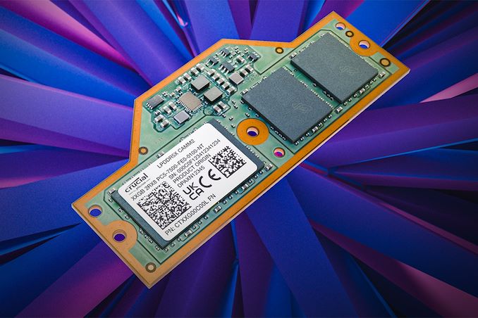
As LPCAMM2 adoption begins, the first retail memory modules are finally starting to hit the retail market, courtesy of Micron. The memory manufacturer has begun selling their LPDDR5X-based LPCAMM2 memory modules under their in-house Crucial brand, making them available on the latter's storefront. Timed to coincide with the release of Lenovo's ThinkPad P1 Gen 7 laptop – the first retail laptop designed to use the memory modules – this marks the de facto start of the eagerly-awaited modular LPDDR5X memory era.
Micron's Low Power Compression Attached Memory Module 2 (LPCAMM2) modules are available in capacities of 32 GB and 64 GB. These are dual-channel modules that feature a 128-bit wide interface, and are based around LPDDR5X memory running at data rates up to 7500 MT/s. This gives a single LPCAMM2 a peak bandwidth of 120 GB/s. Micron is not disclosing the latencies of its LPCAMM2 memory modules, but it says that high data transfer rates of LPDDR5X compensate for the extended timings.
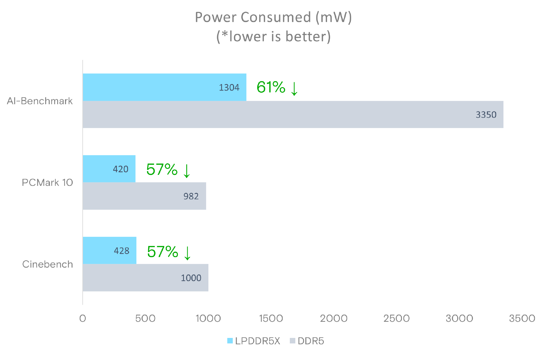
Micron says that LPDDR5X memory offers significantly lower power consumption, with active power per 64-bit bus being 43-58% lower than DDR5 at the same speed, and standby power up to 80% lower. Meanwhile, similar to DDR5 modules, LPCAMM2 modules include a power management IC and voltage regulating circuitry, which provides module manufacturers additional opportunities to reduce power consumption of their products.
Source: Micron LPDDR5X LPCAMM2 Technical Brief
It's worth noting, however, that at least for the first generation of LPCAMM2 modules, system vendors will need to pick between modularity and performance. While soldered-down LPDDR5X memory is available at speeds up to 8533 MT/sec – and with 9600 MT/sec on the horizon – the fastest LPCAMM2 modules planned for this year by both Micron and rival Samsung will be running at 7500 MT/sec. So vendors will have to choose between the flexibility of offering modular LPDDR5X, or the higher bandwidth (and space savings) offered by soldering down their memory.
Micron, for its part, is projecting that 9600 MT/sec LPCAMM2 modules will be available by 2026. Though it's all but certain that faster memory will also be avaialble in the same timeframe.
Micron's Crucial LPDDR5X 32 GB module costs $174.99, whereas a 64 GB module costs $329.99.
Memory
Kioxia's booth at FMS 2024 was a busy one with multiple technology demonstrations keeping visitors occupied. A walk-through of the BiCS 8 manufacturing process was the first to grab my attention. Kioxia and Western Digital announced the sampling of BiCS 8 in March 2023. We had touched briefly upon its CMOS Bonded Array (CBA) scheme in our coverage of Kioxial's 2Tb QLC NAND device and coverage of Western Digital's 128 TB QLC enterprise SSD proof-of-concept demonstration. At Kioxia's booth, we got more insights.
Traditionally, fabrication of flash chips involved placement of the associate logic circuitry (CMOS process) around the periphery of the flash array. The process then moved on to putting the CMOS under the cell array, but the wafer development process was serialized with the CMOS logic getting fabricated first followed by the cell array on top. However, this has some challenges because the cell array requires a high-temperature processing step to ensure higher reliability that can be detrimental to the health of the CMOS logic. Thanks to recent advancements in wafer bonding techniques, the new CBA process allows the CMOS wafer and cell array wafer to be processed independently in parallel and then pieced together, as shown in the models above.
The BiCS 8 3D NAND incorporates 218 layers, compared to 112 layers in BiCS 5 and 162 layers in BiCS 6. The company decided to skip over BiCS 7 (or, rather, it was probably a short-lived generation meant as an internal test vehicle). The generation retains the four-plane charge trap structure of BiCS 6. In its TLC avatar, it is available as a 1 Tbit device. The QLC version is available in two capacities - 1 Tbit and 2 Tbit.
Kioxia also noted that while the number of layers (218) doesn't compare favorably with the latest layer counts from the competition, its lateral scaling / cell shrinkage has enabled it to be competitive in terms of bit density as well as operating speeds (3200 MT/s). For reference, the latest shipping NAND from Micron - the G9 - has 276 layers with a bit density in TLC mode of 21 Gbit/mm2, and operates at up to 3600 MT/s. However, its 232L NAND operates only up to 2400 MT/s and has a bit density of 14.6 Gbit/mm2.
It must be noted that the CBA hybrid bonding process has advantages over the current processes used by other vendors - including Micron's CMOS under array (CuA) and SK hynix's 4D PUC (periphery-under-chip) developed in the late 2010s. It is expected that other NAND vendors will also move eventually to some variant of the hybrid bonding scheme used by Kioxia.
Storage
As LPCAMM2 adoption begins, the first retail memory modules are finally starting to hit the retail market, courtesy of Micron. The memory manufacturer has begun selling their LPDDR5X-based LPCAMM2 memory modules under their in-house Crucial brand, making them available on the latter's storefront. Timed to coincide with the release of Lenovo's ThinkPad P1 Gen 7 laptop – the first retail laptop designed to use the memory modules – this marks the de facto start of the eagerly-awaited modular LPDDR5X memory era.
Micron's Low Power Compression Attached Memory Module 2 (LPCAMM2) modules are available in capacities of 32 GB and 64 GB. These are dual-channel modules that feature a 128-bit wide interface, and are based around LPDDR5X memory running at data rates up to 7500 MT/s. This gives a single LPCAMM2 a peak bandwidth of 120 GB/s. Micron is not disclosing the latencies of its LPCAMM2 memory modules, but it says that high data transfer rates of LPDDR5X compensate for the extended timings.
Micron says that LPDDR5X memory offers significantly lower power consumption, with active power per 64-bit bus being 43-58% lower than DDR5 at the same speed, and standby power up to 80% lower. Meanwhile, similar to DDR5 modules, LPCAMM2 modules include a power management IC and voltage regulating circuitry, which provides module manufacturers additional opportunities to reduce power consumption of their products.
Source: Micron LPDDR5X LPCAMM2 Technical Brief
It's worth noting, however, that at least for the first generation of LPCAMM2 modules, system vendors will need to pick between modularity and performance. While soldered-down LPDDR5X memory is available at speeds up to 8533 MT/sec – and with 9600 MT/sec on the horizon – the fastest LPCAMM2 modules planned for this year by both Micron and rival Samsung will be running at 7500 MT/sec. So vendors will have to choose between the flexibility of offering modular LPDDR5X, or the higher bandwidth (and space savings) offered by soldering down their memory.
Micron, for its part, is projecting that 9600 MT/sec LPCAMM2 modules will be available by 2026. Though it's all but certain that faster memory will also be avaialble in the same timeframe.
Micron's Crucial LPDDR5X 32 GB module costs $174.99, whereas a 64 GB module costs $329.99.
Memory
In an unexpected move, Intel has announced plans to phase out the boxed versions of its enthusiasts-class 13th Generation Core 'Raptor Lake' processors. According to a product change notification (PCN) published by the company last month, Intel plans to stop shipping these desktop CPUs by late June. In its place will remain Intel's existing lineup of boxed 14th Generation Core processors, which are based on the same 'Raptor Lake' silicon and typically carry higher performance for similar prices.
Intel customers and distributors interested in getting boxed versions 13th Generation Core i5-13600K/KF, Core i7-13700K/KF, and Core i9-13900K/KF/KS 'Raptor Lake' processors with unlocked multiplier should place their orders by May 24, 2024. The company will ship these units by June 28, 2024. Meanwhile, the PCN does not mention any change to the availability of tray versions of these CPUs, which are sold to OEMs and wholesalers.
The impending discontinuation of Intel's boxed 13th Generation Core processors comes as the company's current 14th Generation product line, 'Raptor Lake Refresh' is largely a rehash of the same silicon at slightly higher clockspeeds. Case in point: all of the discontinued SKUs are based on Intel's B0 Raptor Lake silicon, which is still being used for their 14th Gen counterparts. So Intel has not discontinued producing any Raptor Lake silicon; only the number of retail SKUs is getting cut-down.
As outlined in our 14th Generation Core/Raptor Lake Refresh review, the 14th Gen chips largely make their 13th Gen counterparts redundant, offering better performance at every tier for the same list price. And with virtually all current generation motherboards supporting both generation of chips, apparently Intel feels there's little reason to keep around what's essentially older, slower SKUs of the same silicon.
Interestingly, the retirement of the enthusiast-class 13th Generation Core chips is coming before Intel discontinues their even older 12th Generation Core 'Alder Lake' processors. 12th Gen chips are still available to this day in both boxed and tray versions, and the Alder Lake silicon itself is still widely in use in multiple product families. So even though Alder Lake shares the same platform as Raptor Lake, the chips based on that silicon haven't been rendered redundant in the same way that 13th Gen Core chips have.
Ultimately, it would seem that Intel is intent on consolidating and simplifying its boxed retail chip offerings by retiring their near-duplicate SKUs. Which for PC buyers could present a minor opportunity for a deal, as retailers work to sell off their remaining 13th Gen enthusiast chips.
CPUs
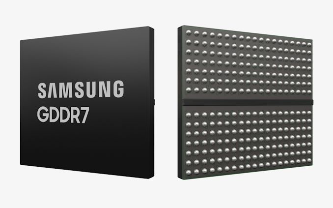
Now that JEDEC has published specification of GDDR7 memory, memory manufacturers are beginning to announce their initial products. The first out of the gate for this generation is Samsung, which has has quietly added its GDDR7 products to its official product catalog.
For now, Samsung lists two GDDR7 devices on its website: 16 Gbit chips rated for an up to 28 GT/s data transfer rate and a faster version running at up to 32 GT/s data transfer rate (which is in line with initial parts that Samsung announced in mid-2023). The chips feature a 512M x32 organization and come in a 266-pin FBGA packaging. The chips are already sampling, so Samsung's customers – GPU vendors, AI inference vendors, network product vendors, and the like – should already have GDDR7 chips in their labs.
The GDDR7 specification promises the maximum per-chip capacity of 64 Gbit (8 GB) and data transfer rates of 48 GT/s. Meanwhile, first generation GDDR7 chips (as announced so far) will feature a rather moderate capacity of 16 Gbit (2 GB) and a data transfer rate of up to 32 GT/s.
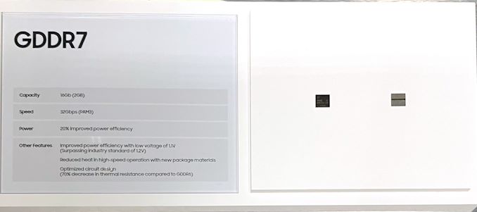
Performance-wise, the first generation of GDDR7 should provide a significant improvement in memory bandwidth over GDDR6 and GDDR6X. However capacity/density improvements will not come until memory manufacturers move to their next generation EUV-based process nodes. As a result, the first GDDR7-based graphics cards are unlikely to sport any memory capacity improvements. Though looking a bit farther down the road, Samsung and SK Hynix have previously told Tom's Hardware that they intend to reach mass production of 24 Gbit GDDR7 chips in 2025.
Otherwise, it is noteworthy that SK Hynix also demonstrated its GDDR7 chips at NVIDIA's GTC last week. So Samsung's competition should be close behind in delivering samples, and eventually mass production memory.
Source: Samsung (via @harukaze5719)
Memory
In an unexpected move, Intel has announced plans to phase out the boxed versions of its enthusiasts-class 13th Generation Core 'Raptor Lake' processors. According to a product change notification (PCN) published by the company last month, Intel plans to stop shipping these desktop CPUs by late June. In its place will remain Intel's existing lineup of boxed 14th Generation Core processors, which are based on the same 'Raptor Lake' silicon and typically carry higher performance for similar prices.
Intel customers and distributors interested in getting boxed versions 13th Generation Core i5-13600K/KF, Core i7-13700K/KF, and Core i9-13900K/KF/KS 'Raptor Lake' processors with unlocked multiplier should place their orders by May 24, 2024. The company will ship these units by June 28, 2024. Meanwhile, the PCN does not mention any change to the availability of tray versions of these CPUs, which are sold to OEMs and wholesalers.
The impending discontinuation of Intel's boxed 13th Generation Core processors comes as the company's current 14th Generation product line, 'Raptor Lake Refresh' is largely a rehash of the same silicon at slightly higher clockspeeds. Case in point: all of the discontinued SKUs are based on Intel's B0 Raptor Lake silicon, which is still being used for their 14th Gen counterparts. So Intel has not discontinued producing any Raptor Lake silicon; only the number of retail SKUs is getting cut-down.
As outlined in our 14th Generation Core/Raptor Lake Refresh review, the 14th Gen chips largely make their 13th Gen counterparts redundant, offering better performance at every tier for the same list price. And with virtually all current generation motherboards supporting both generation of chips, apparently Intel feels there's little reason to keep around what's essentially older, slower SKUs of the same silicon.
Interestingly, the retirement of the enthusiast-class 13th Generation Core chips is coming before Intel discontinues their even older 12th Generation Core 'Alder Lake' processors. 12th Gen chips are still available to this day in both boxed and tray versions, and the Alder Lake silicon itself is still widely in use in multiple product families. So even though Alder Lake shares the same platform as Raptor Lake, the chips based on that silicon haven't been rendered redundant in the same way that 13th Gen Core chips have.
Ultimately, it would seem that Intel is intent on consolidating and simplifying its boxed retail chip offerings by retiring their near-duplicate SKUs. Which for PC buyers could present a minor opportunity for a deal, as retailers work to sell off their remaining 13th Gen enthusiast chips.
CPUs
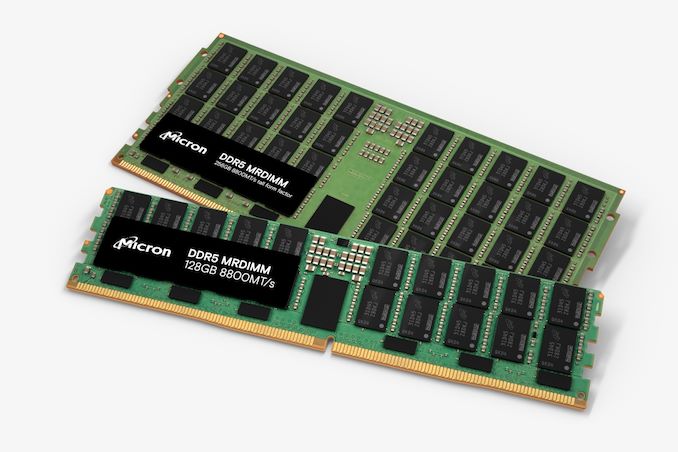
Following a relative lull in the desktop memory industry in the previous decade, the past few years have seen a flurry of new memory standards and form factors enter development. Joining the traditional DIMM/SO-DIMM form factors, we've seen the introduction of space-efficient DDR5 CAMM2s, their LPDDR5-based counterpart the LPCAMM2, and the high-clockspeed optimized CUDIMM. But JEDEC, the industry organization behind these efforts, is not done there. In a press release sent out at the start of the week, the group announced that it is working on standards for DDR5 Multiplexed Rank DIMMs (MRDIMM) for servers, as well as an updated LPCAMM standard to go with next-generation LPDDR6 memory.
Just last week Micron introduced the industry's first DDR5 MRDIMMs, which are timed to launch alongside Intel's Xeon 6 server platforms. But while Intel and its partners are moving full steam ahead on MRDIMMs, the MRDIMM specification has not been fully ratified by JEDEC itself. All told, it's not unusual to see Intel pushing the envelope here on new memory technologies (the company is big enough to bootstrap its own ecosystem). But as MRDIMMs are ultimately meant to be more than just a tool for Intel, a proper industry standard is still needed – even if that takes a bit longer.
Under the hood, MRDIMMs continue to use DDR5 components, form-factor, pinout, SPD, power management ICs (PMICs), and thermal sensors. The major change with the technology is the introduction of multiplexing, which combines multiple data signals over a single channel. The MRDIMM standard also adds RCD/DB logic in a bid to boost performance, increase capacity of memory modules up to 256 GB (for now), shrink latencies, and reduce power consumption of high-end memory subsystems. And, perhaps key to MRDIMM adoption, the standard is being implemented as a backwards-compatible extension to traditional DDR5 RDIMMs, meaning that MRDIMM-capable servers can use either RDIMMs or MRDIMMs, depending on how the operator opts to configure the system.
The MRDIMM standard aims to double the peak bandwidth to 12.8 Gbps, increasing pin speed and supporting more than two ranks. Additionally, a "Tall MRDIMM" form factor is in the works (and pictured above), which is designed to allow for higher capacity DIMMs by providing more area for laying down memory chips. Currently, ultra high capacity DIMMs require using expensive, multi-layer DRAM packages that use through-silicon vias (3DS packaging) to attach the individual DRAM dies; a Tall MRDIMM, on the other hand, can just use a larger number of commodity DRAM chips. Overall, the Tall MRDIMM form factor enables twice the number of DRAM single-die packages on the DIMM.
Meanwhile, this week's announcement from JEDEC offers the first significant insight into what to expect from LPDDR6 CAMMs. And despite LPDDR5 CAMMs having barely made it out the door, some significant shifts with LPDDR6 itself means that JEDEC will need to make some major changes to the CAMM standard to accommodate the newer memory type.
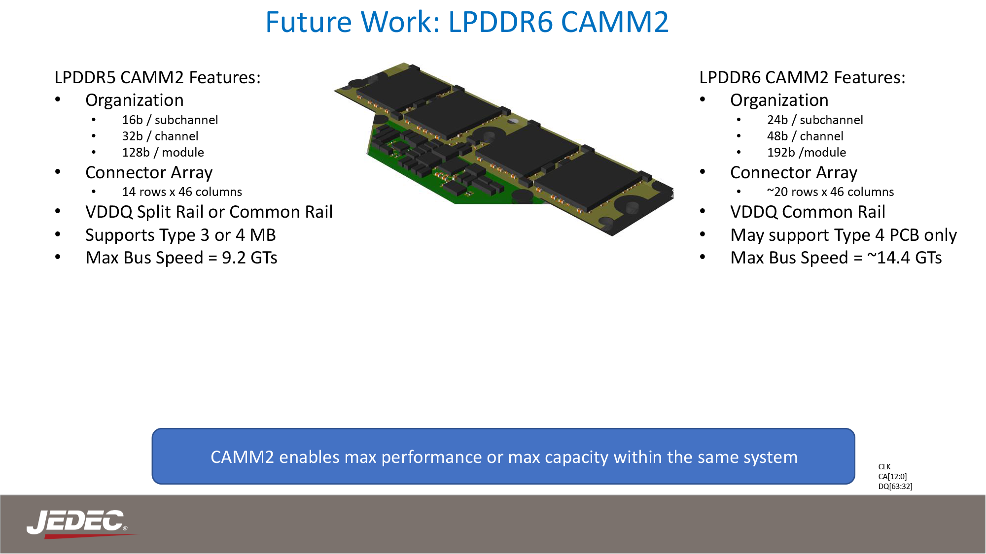
JEDEC Presentation: The CAMM2 Journey and Future Potential
Besides the higher memory clockspeeds allowed by LPDDR6 – JEDEC is targeting data transfer rates of 14.4 GT/s and higher – the new memory form-factor will also incorporate an altogether new connector array. This is to accommodate LPDDR6's wider memory bus, which sees the channel width of an individual memory chip grow from 16-bits wide to 24-bits wide. As a result, the current LPCAMM design, which is intended to match the PC standard of a cumulative 128-bit (16x8) design needs to be reconfigured to match LPDDR6's alterations.
Ultimately, JEDEC is targeting a 24-bit subhannel/48-bit channel design, which will result in a 192-bit wide LPCAMM. While the LPCAMM connector itself is set to grow from 14 rows of pins to possibly as high as 20. New memory technologies typically require new DIMMs to begin with, so it's important to clarify that this is not unexpected, but at th... Memory

![]()
In addition to revealing its roadmap and plans concerning its current leading-edge process technologies, TSMC also shared progress of its N2 node as part of its Symposiums 2024. The company's first 2nm-class fabrication node, and predominantly featuring gate-all-around transistors, according to TSMC N2 has almost achieved its target performance and yield goals, which places it on track to enter high-volume manufacturing in the second half of 2025.
TSMC states that 'N2 development is well on track and N2P is next.' In particular, gate-all-around nanosheet devices currently achieve over 90% of their expected performance, whereas yields of 256 Mb SRAM (32 MB) devices already exceeds 80%, depending on the batch. All of this for a node that is over a year away from mass production.
Meanwhile, average yield of a 256 Mb SRAM was around 70% as of March, 2024, up from around 35% in April, 2023. Device performance has also been improving with higher frequencies being achieved while keeping power consumption in check.
Chip designer interest towards TSMC's first 2nm-class gate-all-around nanosheet transistor-based technology is significant, too. The number of new tape-outs (NTOs) in the first year of N2 is over two-times higher than it was for N5. Though with that said, given TSMC's close working relationship with a handful of high-volume vendors – most notably Appe – NTOs can be a very misleading figure since the first year of a new node at TSMC is capacity constrained, and consequently the bulk of that capacity goes to TSMC's priority partners.
Meanwhile, there were considerably more N5 tapeouts in its second year (some where N5P, of course) and N2 promises to have 2.6X more NTOs in its second year. So the node indeed looks quite promising. In fact, based on TSMC's slides (which we're unfortunately not able to republish), N2 is more popular than N3 in terms of NTOs both in the first and the second years of existence.
When it comes to the second year of N2, in the second half of 2026 TSMC plans to roll out its N2P technology, which promises additional performance and power benefits. N2P is expected to improve frequency by 15% - 20%, reduce power consumption by 30% - 40%, and increase chip density by over 1.15 times compared to N3E, significant benefits to move to all-new GAA nanosheet transistors.
Finally, for those companies that need the best in performance, power, and density, TSMC is poised to offer their A16 process in 2026. That node will also bring in backside power delivery, which will add costs, but is expected to greatly improve performance efficiency and scaling.
Semiconductors

When Western Digital introduced its Ultrastar DC SN861 SSDs earlier this year, the company did not disclose which controller it used for these drives, which made many observers presume that WD was using an in-house controller. But a recent teardown of the drive shows that is not the case; instead, the company is using a controller from Fadu, a South Korean company founded in 2015 that specializes on enterprise-grade turnkey SSD solutions.
The Western Digital Ultrastar DC SN861 SSD is aimed at performance-hungry hyperscale datacenters and enterprise customers which are adopting PCIe Gen5 storage devices these days. And, as uncovered in photos from a recent Storage Review article, the drive is based on Fadu's FC5161 NVMe 2.0-compliant controller. The FC5161 utilizes 16 NAND channels supporting an ONFi 5.0 2400 MT/s interface, and features a combination of enterprise-grade capabilities (OCP Cloud Spec 2.0, SR-IOV, up to 512 name spaces for ZNS support, flexible data placement, NVMe-MI 1.2, advanced security, telemetry, power loss protection) not available on other off-the-shelf controllers – or on any previous Western Digital controllers.
The Ultrastar DC SN861 SSD offers sequential read speeds up to 13.7 GB/s as well as sequential write speeds up to 7.5 GB/s. As for random performance, it boasts with an up to 3.3 million random 4K read IOPS and up to 0.8 million random 4K write IOPS. The drives are available in capacities between 1.6 TB and 7.68 TB with one or three drive writes per day (DWPD) over five years rating as well as in U.2 and E1.S form-factors.
While the two form factors of the SN861 share a similar technical design, Western Digital has tailored each version for distinct workloads: the E1.S supports FDP and performance enhancements specifically for cloud environments. By contrast, the U.2 model is geared towards high-performance enterprise tasks and emerging applications like AI.
Without any doubts, Western Digital's Ultrastar DC SN861 is a feature-rich high-performance enterprise-grade SSD. It has another distinctive feature: a 5W idle power consumption, which is rather low by the standards of enterprise-grade drives (e.g., it is 1W lower compared to the SN840). While the difference with predecessors may be just 1W, hyperscalers deploy thousands of drives and for their TCO every watt counts.
Western Digital's Ultrastar DC SN861 SSDs are now available for purchase to select customers (such as Meta) and to interested parties. Prices are unknown, but they will depend on such factors as volumes.
Sources: Fadu, Storage Review
Storage
Lorem Ipsum is simply dummy text of the printing and typesetting industry. Lorem Ipsum has been the industry's.
Kioxia's booth at FMS 2024 was a busy one with multiple technology demonstrations keeping visitors occupied. A walk-through of the BiCS 8 manufacturing process was the first to grab my attention. Kioxia and Western Digital announced the sampling of BiCS 8 in March 2023. We had touched briefly upon its CMOS Bonded Array (CBA) scheme in our coverage of Kioxial's 2Tb QLC NAND device and coverage of Western Digital's 128 TB QLC enterprise SSD proof-of-concept demonstration. At Kioxia's booth, we got more insights.
Traditionally, fabrication of flash chips involved placement of the associate logic circuitry (CMOS process) around the periphery of the flash array. The process then moved on to putting the CMOS under the cell array, but the wafer development process was serialized with the CMOS logic getting fabricated first followed by the cell array on top. However, this has some challenges because the cell array requires a high-temperature processing step to ensure higher reliability that can be detrimental to the health of the CMOS logic. Thanks to recent advancements in wafer bonding techniques, the new CBA process allows the CMOS wafer and cell array wafer to be processed independently in parallel and then pieced together, as shown in the models above.
The BiCS 8 3D NAND incorporates 218 layers, compared to 112 layers in BiCS 5 and 162 layers in BiCS 6. The company decided to skip over BiCS 7 (or, rather, it was probably a short-lived generation meant as an internal test vehicle). The generation retains the four-plane charge trap structure of BiCS 6. In its TLC avatar, it is available as a 1 Tbit device. The QLC version is available in two capacities - 1 Tbit and 2 Tbit.
Kioxia also noted that while the number of layers (218) doesn't compare favorably with the latest layer counts from the competition, its lateral scaling / cell shrinkage has enabled it to be competitive in terms of bit density as well as operating speeds (3200 MT/s). For reference, the latest shipping NAND from Micron - the G9 - has 276 layers with a bit density in TLC mode of 21 Gbit/mm2, and operates at up to 3600 MT/s. However, its 232L NAND operates only up to 2400 MT/s and has a bit density of 14.6 Gbit/mm2.
It must be noted that the CBA hybrid bonding process has advantages over the current processes used by other vendors - including Micron's CMOS under array (CuA) and SK hynix's 4D PUC (periphery-under-chip) developed in the late 2010s. It is expected that other NAND vendors will also move eventually to some variant of the hybrid bonding scheme used by Kioxia.
Storage

 of cleanroom space, more than twice the size of Amkor's advanced packaging site in Vietnam. Although the company has not disclosed the exact capacity or the specific technologies the facility will support, it is expected to cater to a wide range of industries, including automotive, high-performance computing, and mobile technologies. This suggests the new plant will offer diverse packaging solutions, including traditional, 2.5D, and 3D technologies.</p>
<p>Amkor has collaborated extensively with Apple on the vision and initial setup of the Peoria facility, as Apple is slated to be the facility's first and largest customer, marking a significant commitment from the tech giant. This partnership highlights the importance of the new facility in reinforcing the U.S. semiconductor supply chain and positioning Amkor as a key partner for companies relying on TSMC's manufacturing capabilities. The project is expected to generate around 2,000 jobs and is scheduled to begin operations in 2027. </p>
<h3>SK hynix to Build HBM4 in the U.S.</h3>
<p>This week SK hynix also signed a preliminary agreement with the U.S. government to receive up to $450 million in direct funding and $500 million in loans to build an advanced memory packaging facility in West Lafayette, Indiana. </p>
<p>The proposed facility is scheduled to begin operations in 2028, which means that it will assemble HBM4 or HBM4E memory. Meanwhile, DRAM devices for high bandwidth memory (HBM) stacks will still be produced in South Korea. Nonetheless, packing finished HBM4/HBM4E in the U.S. and possibly integrating these memory modules with high-end processors is a big deal.</p>
<p>In addition to building its packaging plant, SK hynix plans to collaborate with Purdue University and other local research institutions to advance semiconductor technology and packaging innovations. This partnership is intended to bolster research and development in the region, positioning the facility as a hub for AI technology and skilled employment.</p>
<p>Sources: <a href="https://ir.amkor.com/news-releases/news-release-details/amkor-signs-preliminary-memorandum-terms-us-department-commerce">Amkor</a>, <a href="https://news.skhynix.com/preliminary-mou-terms-signed-with-us-doc-for-advanced-packaging-facility-in-indiana/">SK hynix</a></p>
</p> Semiconductors)
 of cleanroom space, more than twice the size of Amkor's advanced packaging site in Vietnam. Although the company has not disclosed the exact capacity or the specific technologies the facility will support, it is expected to cater to a wide range of industries, including automotive, high-performance computing, and mobile technologies. This suggests the new plant will offer diverse packaging solutions, including traditional, 2.5D, and 3D technologies.</p>
<p>Amkor has collaborated extensively with Apple on the vision and initial setup of the Peoria facility, as Apple is slated to be the facility's first and largest customer, marking a significant commitment from the tech giant. This partnership highlights the importance of the new facility in reinforcing the U.S. semiconductor supply chain and positioning Amkor as a key partner for companies relying on TSMC's manufacturing capabilities. The project is expected to generate around 2,000 jobs and is scheduled to begin operations in 2027. </p>
<h3>SK hynix to Build HBM4 in the U.S.</h3>
<p>This week SK hynix also signed a preliminary agreement with the U.S. government to receive up to $450 million in direct funding and $500 million in loans to build an advanced memory packaging facility in West Lafayette, Indiana. </p>
<p>The proposed facility is scheduled to begin operations in 2028, which means that it will assemble HBM4 or HBM4E memory. Meanwhile, DRAM devices for high bandwidth memory (HBM) stacks will still be produced in South Korea. Nonetheless, packing finished HBM4/HBM4E in the U.S. and possibly integrating these memory modules with high-end processors is a big deal.</p>
<p>In addition to building its packaging plant, SK hynix plans to collaborate with Purdue University and other local research institutions to advance semiconductor technology and packaging innovations. This partnership is intended to bolster research and development in the region, positioning the facility as a hub for AI technology and skilled employment.</p>
<p>Sources: <a href="https://ir.amkor.com/news-releases/news-release-details/amkor-signs-preliminary-memorandum-terms-us-department-commerce">Amkor</a>, <a href="https://news.skhynix.com/preliminary-mou-terms-signed-with-us-doc-for-advanced-packaging-facility-in-indiana/">SK hynix</a></p>
</p> Semiconductors | https://compbuddey.blogspot.com/2025/02/us-signs-15b-in-chips-act-agreements_21.html)
 of cleanroom space, more than twice the size of Amkor's advanced packaging site in Vietnam. Although the company has not disclosed the exact capacity or the specific technologies the facility will support, it is expected to cater to a wide range of industries, including automotive, high-performance computing, and mobile technologies. This suggests the new plant will offer diverse packaging solutions, including traditional, 2.5D, and 3D technologies.</p>
<p>Amkor has collaborated extensively with Apple on the vision and initial setup of the Peoria facility, as Apple is slated to be the facility's first and largest customer, marking a significant commitment from the tech giant. This partnership highlights the importance of the new facility in reinforcing the U.S. semiconductor supply chain and positioning Amkor as a key partner for companies relying on TSMC's manufacturing capabilities. The project is expected to generate around 2,000 jobs and is scheduled to begin operations in 2027. </p>
<h3>SK hynix to Build HBM4 in the U.S.</h3>
<p>This week SK hynix also signed a preliminary agreement with the U.S. government to receive up to $450 million in direct funding and $500 million in loans to build an advanced memory packaging facility in West Lafayette, Indiana. </p>
<p>The proposed facility is scheduled to begin operations in 2028, which means that it will assemble HBM4 or HBM4E memory. Meanwhile, DRAM devices for high bandwidth memory (HBM) stacks will still be produced in South Korea. Nonetheless, packing finished HBM4/HBM4E in the U.S. and possibly integrating these memory modules with high-end processors is a big deal.</p>
<p>In addition to building its packaging plant, SK hynix plans to collaborate with Purdue University and other local research institutions to advance semiconductor technology and packaging innovations. This partnership is intended to bolster research and development in the region, positioning the facility as a hub for AI technology and skilled employment.</p>
<p>Sources: <a href="https://ir.amkor.com/news-releases/news-release-details/amkor-signs-preliminary-memorandum-terms-us-department-commerce">Amkor</a>, <a href="https://news.skhynix.com/preliminary-mou-terms-signed-with-us-doc-for-advanced-packaging-facility-in-indiana/">SK hynix</a></p>
</p> Semiconductors&body=https://compbuddey.blogspot.com/2025/02/us-signs-15b-in-chips-act-agreements_21.html)
0 Comments