
It is with great sadness that I find myself penning the hardest news post I’ve ever needed to write here at AnandTech. After over 27 years of covering the wide – and wild – world of computing hardware, today is AnandTech’s final day of publication.
For better or worse, we’ve reached the end of a long journey – one that started with a review of an AMD processor, and has ended with the review of an AMD processor. It’s fittingly poetic, but it is also a testament to the fact that we’ve spent the last 27 years doing what we love, covering the chips that are the lifeblood of the computing industry.
A lot of things have changed in the last quarter-century – in 1997 NVIDIA had yet to even coin the term “GPU” – and we’ve been fortunate to watch the world of hardware continue to evolve over the time period. We’ve gone from boxy desktop computers and laptops that today we’d charitably classify as portable desktops, to pocket computers where even the cheapest budget device puts the fastest PC of 1997 to shame.
The years have also brought some monumental changes to the world of publishing. AnandTech was hardly the first hardware enthusiast website, nor will we be the last. But we were fortunate to thrive in the past couple of decades, when so many of our peers did not, thanks to a combination of hard work, strategic investments in people and products, even more hard work, and the support of our many friends, colleagues, and readers.
Still, few things last forever, and the market for written tech journalism is not what it once was – nor will it ever be again. So, the time has come for AnandTech to wrap up its work, and let the next generation of tech journalists take their place within the zeitgeist.
It has been my immense privilege to write for AnandTech for the past 19 years – and to manage it as its editor-in-chief for the past decade. And while I carry more than a bit of remorse in being AnandTech’s final boss, I can at least take pride in everything we’ve accomplished over the years, whether it’s lauding some legendary products, writing technology primers that still remain relevant today, or watching new stars rise in expected places. There is still more that I had wanted AnandTech to do, but after 21,500 articles, this was a good start.
And while the AnandTech staff is riding off into the sunset, I am happy to report that the site itself won’t be going anywhere for a while. Our publisher, Future PLC, will be keeping the AnandTech website and its many articles live indefinitely. So that all of the content we’ve created over the years remains accessible and citable. Even without new articles to add to the collection, I expect that many of the things we’ve written over the past couple of decades will remain relevant for years to come – and remain accessible just as long.
The AnandTech Forums will also continue to be operated by Future’s community team and our dedicated troop of moderators. With forum threads going back to 1999 (and some active members just as long), the forums have a history almost as long and as storied as AnandTech itself (wounded monitor children, anyone?). So even when AnandTech is no longer publishing articles, we’ll still have a place for everyone to talk about the latest in technology – and have those discussions last longer than 48 hours.
Finally, for everyone who still needs their technical writing fix, our formidable opposition of the last 27 years and fellow Future brand, Tom’s Hardware, is continuing to cover the world of technology. There are a couple of familiar AnandTech faces already over there providing their accumulated expertise, and the site will continue doing its best to provide a written take on technology news.
As I look back on everything AnandTech has accomplished over the past 27 years, there are more than a few people, groups, and companies that I would like to thank on behalf of both myself and AnandTech as a whole.
First and foremost, I cannot thank enough all the editors who have worked for AnandTech over the years. T... Site Updates

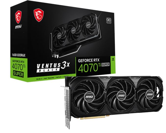
As GPU families enter the later part of their lifecycles, we often see chip manufacturers start to offload stockpiles of salvaged chips that, for one reason or another, didn't make the grade for the tier of cards they normally are used in. These recovered chips are fairly unremarkable overall, but they are unsold silicon that still works and has economic value, leading to them being used in lower-tier cards so that they can be sold. And, judging by the appearance of a new video card design from MSI, it looks like NVIDIA's Ada Lovelace generation of chips has reached that stage, as the Taiwanese video card maker has put out a new GeForce RTX 4070 Ti Super card based on a salvaged AD102 GPU.
Typically based on NVIDIA's AD103 GPU, NVIDIA's GeForce RTX 4070 Ti Super series sits a step below the company's flagship RTX 4080/4090 cards, both of which are based on the bigger and badder AD102 chip. But with some number of AD102 chips inevitably failing to live up to RTX 4080 specifications, rather than being thrown out, these chips can instead be used to make RTX 4070 cards. Which is exactly what MSI has done with their new GeForce RTX 4070 Ti Super Ventus 3X Black OC graphics card.
The card itself is relatively unremarkable – using a binned AD102 chip doesn't come with any advantages, and it should perform just like regular AD103 cards – and for that reason, video card vendors rarely publicly note when they're doing a run of cards with a binned-down version of a bigger chip. However, these larger chips have a tell-tale PCB footprint that usually makes it obvious what's going on. Which, as first noticed by @wxnod, is exactly what's going on with MSI's card.

Ada Lovelace Lineup: MSI GeForce RTX 4070 TiS (AD103), RTX 4070 TiS (AD102), & RTX 4090 (AD102)
The tell, in this case, is the rear board shot provided by MSI. The larger AD102 GPU uses an equally larger mounting bracket, and is paired with a slightly more complex array of filtering capacitors on the back side of the board PCB. Ultimately, since these are visible in MSI's photos of their GeForce RTX 4070 Ti Super Ventus 3X Black OC, it's easy to compare it to other video cards and see that it has exactly the same capacitor layout as MSI's GeForce RTX 4090, thus confirming the use of an AD102 GPU.
Chip curiosities aside, all of NVIDIA GeForce RTX 4070 Ti Super graphics cards – no matter whether they are based on the AD102 or AD103 GPU – come with a GPU with 8,448 active CUDA cores and 16 GB of GDDR6X memory, so it doesn't (typically) matter which chip they carry. Otherwise, compared to a fully-enabled AD102 chip, the RTX 4070 Ti Super specifications are relatively modest, with fewer than half as many CUDA cores, underscoring how the AD102 chip being used in MSI's card is a pretty heavy salvage bin.
As for the rest of the card, MSI GeForce RTX 4070 Ti Super Ventus 3X Black OC is a relatively hefty card overall, with a cooling system to match. Being overclocked, the Ventus also has a slightly higher TDP than normal GeForce RTX 4070 Ti Super cards, weighing in at 295 Watts, or 10 Watts above baseline cards.
Meanwhile, MSI is apparently not the only video card manufacturer using salvaged AD102 chips for GeForce RTX 4070 Ti Super, either. @wxnod has also posted a screenshot obtained on an Inno3D GeForce RTX 4070 Ti Super based on an AD102 GPU.
GPUs
As GPU families enter the later part of their lifecycles, we often see chip manufacturers start to offload stockpiles of salvaged chips that, for one reason or another, didn't make the grade for the tier of cards they normally are used in. These recovered chips are fairly unremarkable overall, but they are unsold silicon that still works and has economic value, leading to them being used in lower-tier cards so that they can be sold. And, judging by the appearance of a new video card design from MSI, it looks like NVIDIA's Ada Lovelace generation of chips has reached that stage, as the Taiwanese video card maker has put out a new GeForce RTX 4070 Ti Super card based on a salvaged AD102 GPU.
Typically based on NVIDIA's AD103 GPU, NVIDIA's GeForce RTX 4070 Ti Super series sits a step below the company's flagship RTX 4080/4090 cards, both of which are based on the bigger and badder AD102 chip. But with some number of AD102 chips inevitably failing to live up to RTX 4080 specifications, rather than being thrown out, these chips can instead be used to make RTX 4070 cards. Which is exactly what MSI has done with their new GeForce RTX 4070 Ti Super Ventus 3X Black OC graphics card.
The card itself is relatively unremarkable – using a binned AD102 chip doesn't come with any advantages, and it should perform just like regular AD103 cards – and for that reason, video card vendors rarely publicly note when they're doing a run of cards with a binned-down version of a bigger chip. However, these larger chips have a tell-tale PCB footprint that usually makes it obvious what's going on. Which, as first noticed by @wxnod, is exactly what's going on with MSI's card.
Ada Lovelace Lineup: MSI GeForce RTX 4070 TiS (AD103), RTX 4070 TiS (AD102), & RTX 4090 (AD102)
The tell, in this case, is the rear board shot provided by MSI. The larger AD102 GPU uses an equally larger mounting bracket, and is paired with a slightly more complex array of filtering capacitors on the back side of the board PCB. Ultimately, since these are visible in MSI's photos of their GeForce RTX 4070 Ti Super Ventus 3X Black OC, it's easy to compare it to other video cards and see that it has exactly the same capacitor layout as MSI's GeForce RTX 4090, thus confirming the use of an AD102 GPU.
Chip curiosities aside, all of NVIDIA GeForce RTX 4070 Ti Super graphics cards – no matter whether they are based on the AD102 or AD103 GPU – come with a GPU with 8,448 active CUDA cores and 16 GB of GDDR6X memory, so it doesn't (typically) matter which chip they carry. Otherwise, compared to a fully-enabled AD102 chip, the RTX 4070 Ti Super specifications are relatively modest, with fewer than half as many CUDA cores, underscoring how the AD102 chip being used in MSI's card is a pretty heavy salvage bin.
As for the rest of the card, MSI GeForce RTX 4070 Ti Super Ventus 3X Black OC is a relatively hefty card overall, with a cooling system to match. Being overclocked, the Ventus also has a slightly higher TDP than normal GeForce RTX 4070 Ti Super cards, weighing in at 295 Watts, or 10 Watts above baseline cards.
Meanwhile, MSI is apparently not the only video card manufacturer using salvaged AD102 chips for GeForce RTX 4070 Ti Super, either. @wxnod has also posted a screenshot obtained on an Inno3D GeForce RTX 4070 Ti Super based on an AD102 GPU.
GPUs
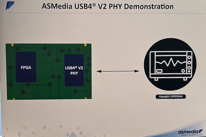
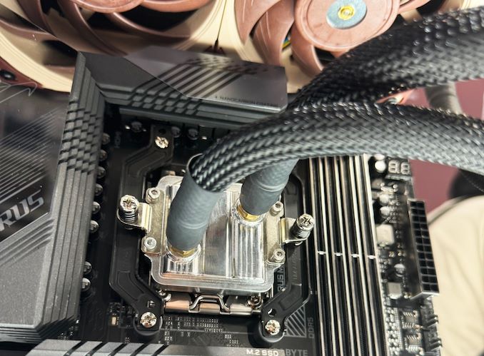
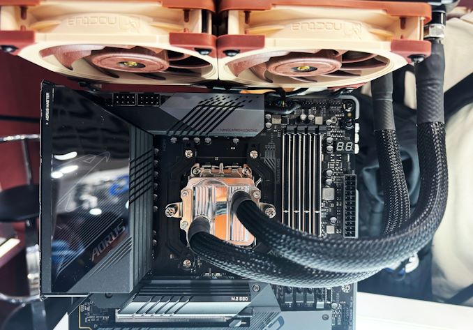
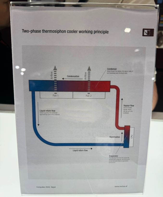
The USB Implementers Forum (USB-IF) introduced USB4 version 2.0 in fall 2022, and it expects systems and devices with the tech to emerge later this year and into next year. These upcoming products will largely rely on Intel's Barlow Ridge controller, a full-featured Thunderbolt 5 controller that goes above and beond the baseline USB4 v2 spec. And though extremely capable, Intel's Thunderbolt controllers are also quite expensive, and Barlow Ridge isn't expected to be any different. Fortunately, for system and device vendors that just need a basic USB4 v2 solution, ASMedia is also working on its own USB4 v2 controller.
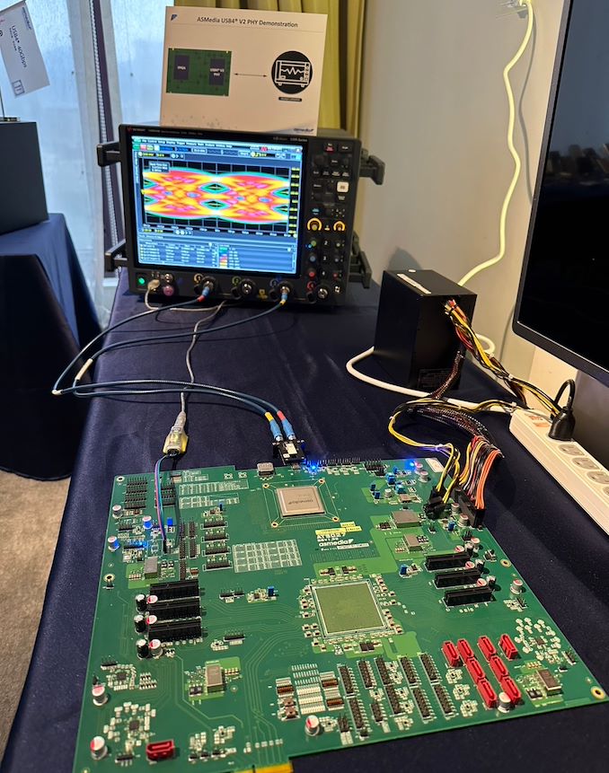
At Computex 2024, ASMedia demonstrated a prototype of its upcoming USB4 v2 physical interface (PHY), which will support USB4 v2's new Gen 4 (160Gbps) data rates and the associated PAM-3 signal encoding. The prototype was implemented using an FPGA, as the company yet has to tape out the completed controller.
Ultimately, the purpose of showing off a FPGA-based PHY at Computex was to allow ASMedia to demonstrate their current PHY design. With the shift to PAM-3 encoding for USB4 v2, ASMedia (and the rest of the USB ecosystem) must develop significantly more complex controllers – and there's no part of that more critical than a solid and reliable PHY design.
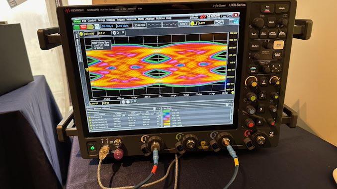
As part of their demonstration, ASMedia had a classic eye diagram display. The eye diagram demoed has a clear opening in the center, which is indicative of good signal integrity, as the larger the eye opening, the less distortion and noise in the signal. The horizontal width of the eye opening represents the time window in which the signal can be sampled correctly, so the relatively narrow horizontal spread of the eye opening suggests that there is minimal jitter, meaning the signal transitions are consistent and predictable. Finally, the vertical height of the eye opening indicates the signal amplitude and the rather tall eye opening suggests a higher signal-to-noise ratio (SNR), meaning that the signal is strong compared to any noise present.
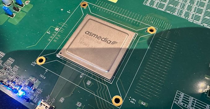
ASMedia itself is one of the major suppliers for discrete USB controllers, so the availability of ASMedia's USB4 v2 chip is crucial for adoption of the standard in general. While Intel will spearhead the industry with their Barlow Ridge Thunderbolt 5/USB4 v2 controller, ASMedia's controller is poised to end up in a far larger range of devices. So the importance of the company's USB4 v2 PHY demo is hard to overstate.
Demos aside, ASMedia is hoping to tape the chip out soon. If all goes well, the company expects their first USB4 v2 controllers to hit the market some time in the second half of 2025.

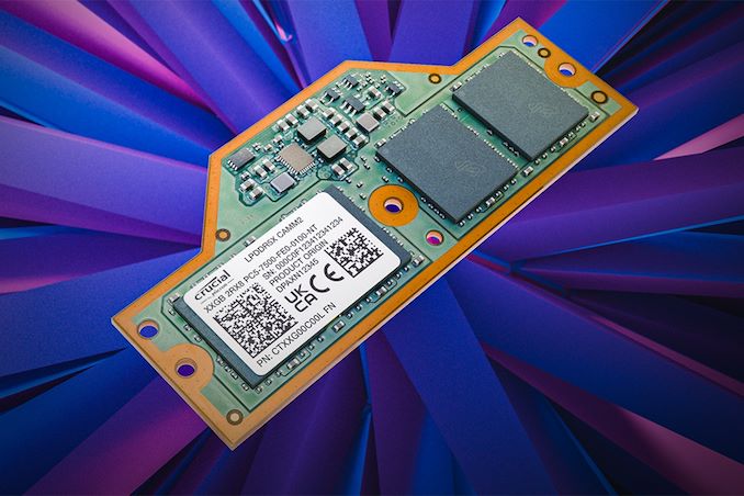
As LPCAMM2 adoption begins, the first retail memory modules are finally starting to hit the retail market, courtesy of Micron. The memory manufacturer has begun selling their LPDDR5X-based LPCAMM2 memory modules under their in-house Crucial brand, making them available on the latter's storefront. Timed to coincide with the release of Lenovo's ThinkPad P1 Gen 7 laptop – the first retail laptop designed to use the memory modules – this marks the de facto start of the eagerly-awaited modular LPDDR5X memory era.
Micron's Low Power Compression Attached Memory Module 2 (LPCAMM2) modules are available in capacities of 32 GB and 64 GB. These are dual-channel modules that feature a 128-bit wide interface, and are based around LPDDR5X memory running at data rates up to 7500 MT/s. This gives a single LPCAMM2 a peak bandwidth of 120 GB/s. Micron is not disclosing the latencies of its LPCAMM2 memory modules, but it says that high data transfer rates of LPDDR5X compensate for the extended timings.
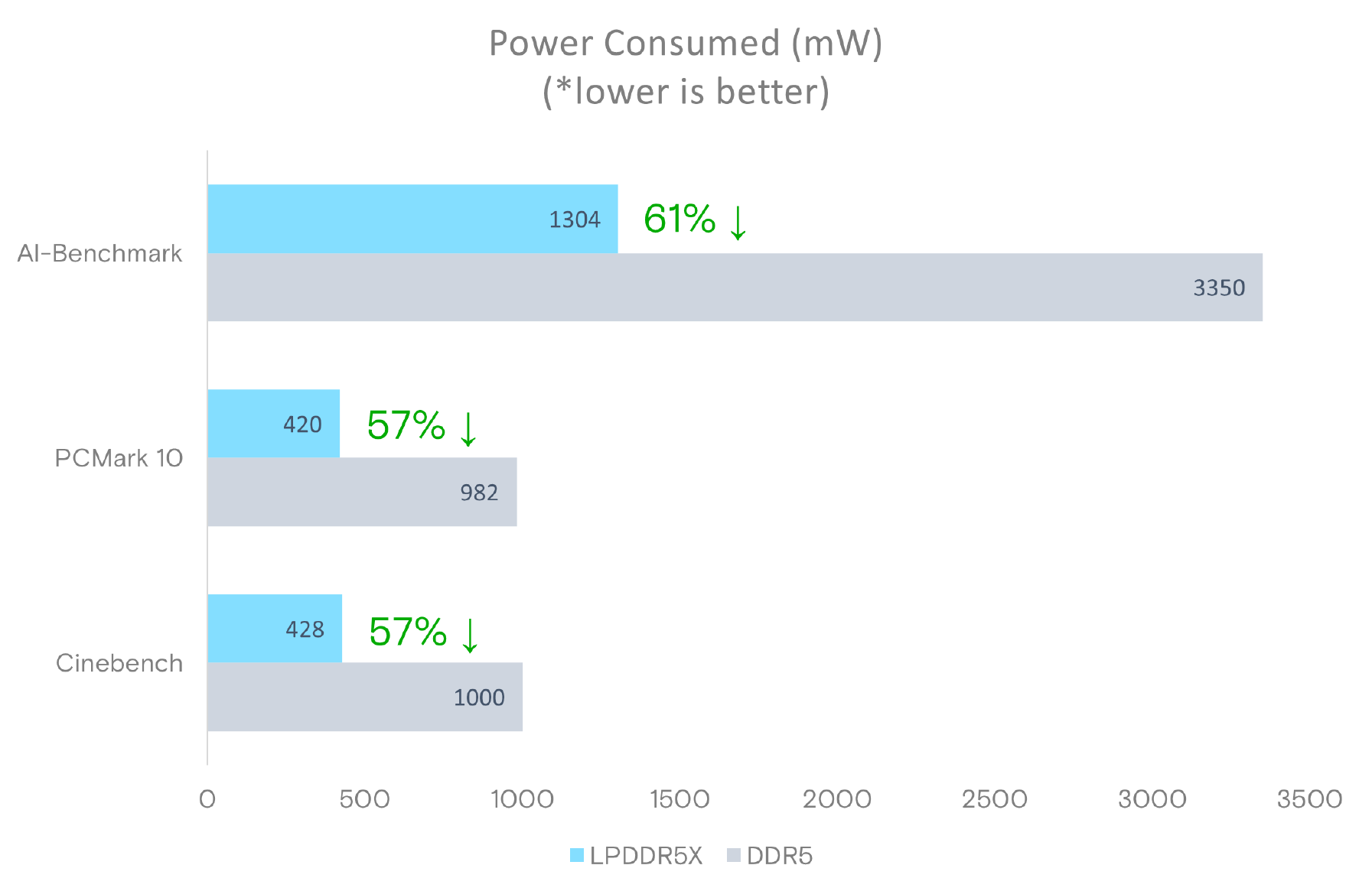
Micron says that LPDDR5X memory offers significantly lower power consumption, with active power per 64-bit bus being 43-58% lower than DDR5 at the same speed, and standby power up to 80% lower. Meanwhile, similar to DDR5 modules, LPCAMM2 modules include a power management IC and voltage regulating circuitry, which provides module manufacturers additional opportunities to reduce power consumption of their products.
Source: Micron LPDDR5X LPCAMM2 Technical Brief
It's worth noting, however, that at least for the first generation of LPCAMM2 modules, system vendors will need to pick between modularity and performance. While soldered-down LPDDR5X memory is available at speeds up to 8533 MT/sec – and with 9600 MT/sec on the horizon – the fastest LPCAMM2 modules planned for this year by both Micron and rival Samsung will be running at 7500 MT/sec. So vendors will have to choose between the flexibility of offering modular LPDDR5X, or the higher bandwidth (and space savings) offered by soldering down their memory.
Micron, for its part, is projecting that 9600 MT/sec LPCAMM2 modules will be available by 2026. Though it's all but certain that faster memory will also be avaialble in the same timeframe.
Micron's Crucial LPDDR5X 32 GB module costs $174.99, whereas a 64 GB module costs $329.99.
Memory
Lorem Ipsum is simply dummy text of the printing and typesetting industry. Lorem Ipsum has been the industry's.


, the forums have a history almost as long and as storied as AnandTech itself (wounded monitor children, anyone?). So even when AnandTech is no longer publishing articles, we’ll still have a place for everyone to talk about the latest in technology – and have those discussions last longer than 48 hours.</p>
<p align="center"><a href="https://www.anandtech.com/show/21542/end-of-the-road-an-anandtech-farewell"><img alt="" src="https://images.anandtech.com/doci/21542/AT_Forums.png" style="width: 100%;" /></a></p>
<p>Finally, for everyone who still needs their technical writing fix, our formidable opposition of the last 27 years and fellow Future brand, <a href="https://www.tomshardware.com/">Tom’s Hardware</a>, is continuing to cover the world of technology. There are a couple of familiar AnandTech faces already over there providing their accumulated expertise, and the site will continue doing its best to provide a written take on technology news.</p>
<h3>So Many Thank Yous</h3>
<p>As I look back on everything AnandTech has accomplished over the past 27 years, there are more than a few people, groups, and companies that I would like to thank on behalf of both myself and AnandTech as a whole.</p>
<p>First and foremost, I cannot thank enough all the editors who have worked for AnandTech over the years. T... Site Updates)
, the forums have a history almost as long and as storied as AnandTech itself (wounded monitor children, anyone?). So even when AnandTech is no longer publishing articles, we’ll still have a place for everyone to talk about the latest in technology – and have those discussions last longer than 48 hours.</p>
<p align="center"><a href="https://www.anandtech.com/show/21542/end-of-the-road-an-anandtech-farewell"><img alt="" src="https://images.anandtech.com/doci/21542/AT_Forums.png" style="width: 100%;" /></a></p>
<p>Finally, for everyone who still needs their technical writing fix, our formidable opposition of the last 27 years and fellow Future brand, <a href="https://www.tomshardware.com/">Tom’s Hardware</a>, is continuing to cover the world of technology. There are a couple of familiar AnandTech faces already over there providing their accumulated expertise, and the site will continue doing its best to provide a written take on technology news.</p>
<h3>So Many Thank Yous</h3>
<p>As I look back on everything AnandTech has accomplished over the past 27 years, there are more than a few people, groups, and companies that I would like to thank on behalf of both myself and AnandTech as a whole.</p>
<p>First and foremost, I cannot thank enough all the editors who have worked for AnandTech over the years. T... Site Updates | https://compbuddey.blogspot.com/2025/02/end-of-road-anandtech-farewell-it-is_17.html)
, the forums have a history almost as long and as storied as AnandTech itself (wounded monitor children, anyone?). So even when AnandTech is no longer publishing articles, we’ll still have a place for everyone to talk about the latest in technology – and have those discussions last longer than 48 hours.</p>
<p align="center"><a href="https://www.anandtech.com/show/21542/end-of-the-road-an-anandtech-farewell"><img alt="" src="https://images.anandtech.com/doci/21542/AT_Forums.png" style="width: 100%;" /></a></p>
<p>Finally, for everyone who still needs their technical writing fix, our formidable opposition of the last 27 years and fellow Future brand, <a href="https://www.tomshardware.com/">Tom’s Hardware</a>, is continuing to cover the world of technology. There are a couple of familiar AnandTech faces already over there providing their accumulated expertise, and the site will continue doing its best to provide a written take on technology news.</p>
<h3>So Many Thank Yous</h3>
<p>As I look back on everything AnandTech has accomplished over the past 27 years, there are more than a few people, groups, and companies that I would like to thank on behalf of both myself and AnandTech as a whole.</p>
<p>First and foremost, I cannot thank enough all the editors who have worked for AnandTech over the years. T... Site Updates&body=https://compbuddey.blogspot.com/2025/02/end-of-road-anandtech-farewell-it-is_17.html)
0 Comments