
The CXL consortium has had a regular presence at FMS (which rechristened itself from 'Flash Memory Summit' to the 'Future of Memory and Storage' this year). Back at FMS 2022, the company had announced v3.0 of the CXL specifications. This was followed by CXL 3.1's introduction at Supercomputing 2023. Having started off as a host to device interconnect standard, it had slowly subsumed other competing standards such as OpenCAPI and Gen-Z. As a result, the specifications started to encompass a wide variety of use-cases by building a protocol on top of the the ubiquitous PCIe expansion bus. The CXL consortium comprises of heavyweights such as AMD and Intel, as well as a large number of startup companies attempting to play in different segments on the device side. At FMS 2024, CXL had a prime position in the booth demos of many vendors.
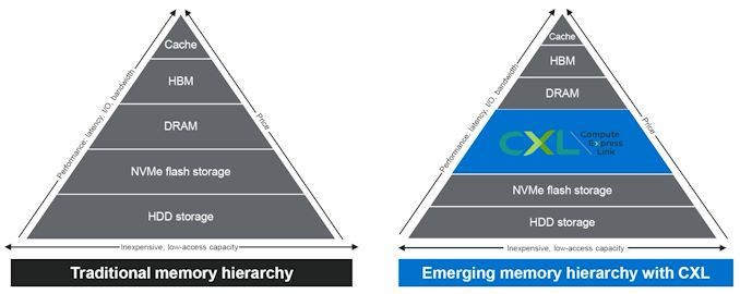
The migration of server platforms from DDR4 to DDR5, along with the rise of workloads demanding large RAM capacity (but not particularly sensitive to either memory bandwidth or latency), has opened up memory expansion modules as one of the first set of widely available CXL devices. Over the last couple of years, we have had product announcements from Samsung and Micron in this area.
At FMS 2024, SK hynix was showing off their DDR5-based CMM-DDR5 CXL memory module with a 128 GB capacity. The company was also detailing their associated Heterogeneous Memory Software Development Kit (HMSDK) - a set of libraries and tools at both the kernel and user levels aimed at increasing the ease of use of CXL memory. This is achieved in part by considering the memory pyramid / hierarchy and relocating the data between the server's main memory (DRAM) and the CXL device based on usage frequency.
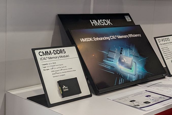
The CMM-DDR5 CXL memory module comes in the SDFF form-factor (E3.S 2T) with a PCIe 3.0 x8 host interface. The internal memory is based on 1α technology DRAM, and the device promises DDR5-class bandwidth and latency within a single NUMA hop. As these memory modules are meant to be used in datacenters and enterprises, the firmware includes features for RAS (reliability, availability, and serviceability) along with secure boot and other management features.
SK hynix was also demonstrating Niagara 2.0 - a hardware solution (currently based on FPGAs) to enable memory pooling and sharing - i.e, connecting multiple CXL memories to allow different hosts (CPUs and GPUs) to optimally share their capacity. The previous version only allowed capacity sharing, but the latest version enables sharing of data also. SK hynix had presented these solutions at the CXL DevCon 2024 earlier this year, but some progress seems to have been made in finalizing the specifications of the CMM-DDR5 at FMS 2024.
Micron had unveiled the CZ120 CXL Memory Expansion Module last year based on the Microchip SMC 2000 series CXL memory controller. At FMS 2024, Micron and Microchip had a demonstration of the module on a Granite Rapids server.
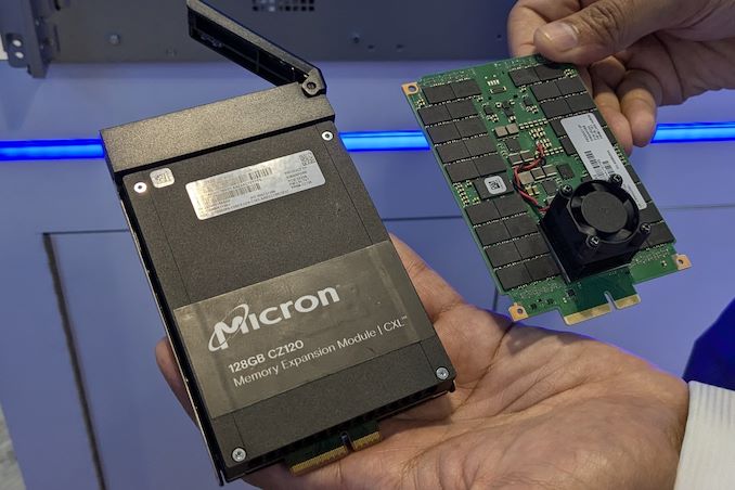
Additional insights into the SMC 2000 controller were also provided.
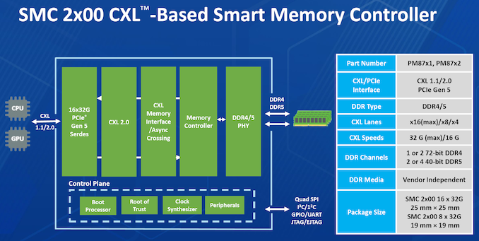
The CXL memory controller also incorporates DRAM die failure handling, and Microchip also provides diagnostics and debug tools to analyze failed modules. The memory controller also supports ECC, which forms part of the enterprise... Storage


G.Skill on Tuesday introduced its ultra-low-latency DDR5-6400 memory modules that feature a CAS latency of 30 clocks, which appears to be the industry's most aggressive timings yet for DDR5-6400 sticks. The modules will be available for both AMD and Intel CPU-based systems.
With every new generation of DDR memory comes an increase in data transfer rates and an extension of relative latencies. While for the vast majority of applications, the increased bandwidth offsets the performance impact of higher timings, there are applications that favor low latencies. However, shrinking latencies is sometimes harder than increasing data transfer rates, which is why low-latency modules are rare.
Nonetheless, G.Skill has apparently managed to cherry-pick enough DDR5 memory chips and build appropriate printed circuit boards to produce DDR5-6400 modules with CL30 timings, which are substantially lower than the CL46 timings recommended by JEDEC for this speed bin. This means that while JEDEC-standard modules have an absolute latency of 14.375 ns, G.Skill's modules can boast a latency of just 9.375 ns – an approximately 35% decrease.
G.Skill's DDR5-6400 CL30 39-39-102 modules have a capacity of 16 GB and will be available in 32 GB dual-channel kits, though the company does not disclose voltages, which are likely considerably higher than those standardized by JEDEC.
The company plans to make its DDR5-6400 modules available both for AMD systems with EXPO profiles (Trident Z5 Neo RGB and Trident Z5 Royal Neo) and for Intel-powered PCs with XMP 3.0 profiles (Trident Z5 RGB and Trident Z5 Royal). For AMD AM5 systems that have a practical limitation of 6000 MT/s – 6400 MT/s for DDR5 memory (as this is roughly as fast as AMD's Infinity Fabric can operate at with a 1:1 ratio), the new modules will be particularly beneficial for AMD's Ryzen 7000 and Ryzen 9000-series processors.
G.Skill notes that since its modules are non-standard, they will not work with all systems but will operate on high-end motherboards with properly cooled CPUs.
The new ultra-low-latency memory kits will be available worldwide from G.Skill's partners starting in late August 2024. The company did not disclose the pricing of these modules, but since we are talking about premium products that boast unique specifications, they are likely to be priced accordingly.
Memory
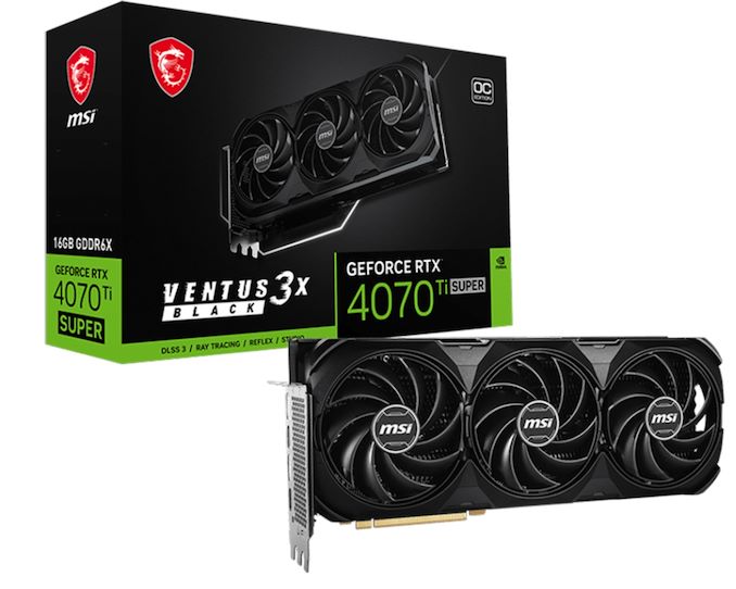
As GPU families enter the later part of their lifecycles, we often see chip manufacturers start to offload stockpiles of salvaged chips that, for one reason or another, didn't make the grade for the tier of cards they normally are used in. These recovered chips are fairly unremarkable overall, but they are unsold silicon that still works and has economic value, leading to them being used in lower-tier cards so that they can be sold. And, judging by the appearance of a new video card design from MSI, it looks like NVIDIA's Ada Lovelace generation of chips has reached that stage, as the Taiwanese video card maker has put out a new GeForce RTX 4070 Ti Super card based on a salvaged AD102 GPU.
Typically based on NVIDIA's AD103 GPU, NVIDIA's GeForce RTX 4070 Ti Super series sits a step below the company's flagship RTX 4080/4090 cards, both of which are based on the bigger and badder AD102 chip. But with some number of AD102 chips inevitably failing to live up to RTX 4080 specifications, rather than being thrown out, these chips can instead be used to make RTX 4070 cards. Which is exactly what MSI has done with their new GeForce RTX 4070 Ti Super Ventus 3X Black OC graphics card.
The card itself is relatively unremarkable – using a binned AD102 chip doesn't come with any advantages, and it should perform just like regular AD103 cards – and for that reason, video card vendors rarely publicly note when they're doing a run of cards with a binned-down version of a bigger chip. However, these larger chips have a tell-tale PCB footprint that usually makes it obvious what's going on. Which, as first noticed by @wxnod, is exactly what's going on with MSI's card.
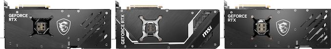
Ada Lovelace Lineup: MSI GeForce RTX 4070 TiS (AD103), RTX 4070 TiS (AD102), & RTX 4090 (AD102)
The tell, in this case, is the rear board shot provided by MSI. The larger AD102 GPU uses an equally larger mounting bracket, and is paired with a slightly more complex array of filtering capacitors on the back side of the board PCB. Ultimately, since these are visible in MSI's photos of their GeForce RTX 4070 Ti Super Ventus 3X Black OC, it's easy to compare it to other video cards and see that it has exactly the same capacitor layout as MSI's GeForce RTX 4090, thus confirming the use of an AD102 GPU.
Chip curiosities aside, all of NVIDIA GeForce RTX 4070 Ti Super graphics cards – no matter whether they are based on the AD102 or AD103 GPU – come with a GPU with 8,448 active CUDA cores and 16 GB of GDDR6X memory, so it doesn't (typically) matter which chip they carry. Otherwise, compared to a fully-enabled AD102 chip, the RTX 4070 Ti Super specifications are relatively modest, with fewer than half as many CUDA cores, underscoring how the AD102 chip being used in MSI's card is a pretty heavy salvage bin.
As for the rest of the card, MSI GeForce RTX 4070 Ti Super Ventus 3X Black OC is a relatively hefty card overall, with a cooling system to match. Being overclocked, the Ventus also has a slightly higher TDP than normal GeForce RTX 4070 Ti Super cards, weighing in at 295 Watts, or 10 Watts above baseline cards.
Meanwhile, MSI is apparently not the only video card manufacturer using salvaged AD102 chips for GeForce RTX 4070 Ti Super, either. @wxnod has also posted a screenshot obtained on an Inno3D GeForce RTX 4070 Ti Super based on an AD102 GPU.
GPUs
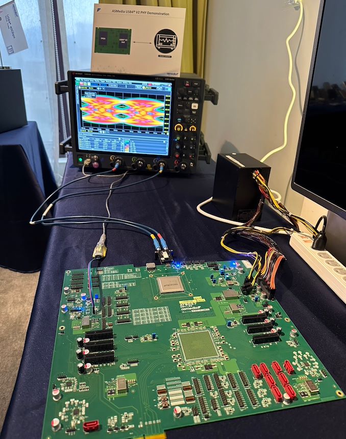
The USB Implementers Forum (USB-IF) introduced USB4 version 2.0 in fall 2022, and it expects systems and devices with the tech to emerge later this year and into next year. These upcoming products will largely rely on Intel's Barlow Ridge controller, a full-featured Thunderbolt 5 controller that goes above and beond the baseline USB4 v2 spec. And though extremely capable, Intel's Thunderbolt controllers are also quite expensive, and Barlow Ridge isn't expected to be any different. Fortunately, for system and device vendors that just need a basic USB4 v2 solution, ASMedia is also working on its own USB4 v2 controller.
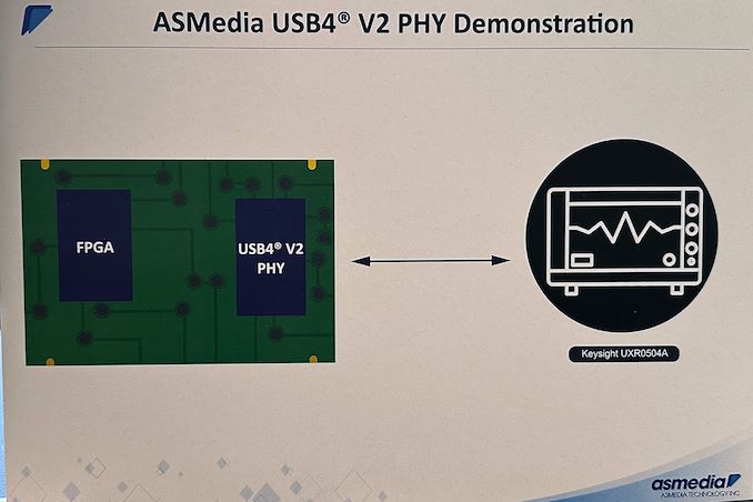
At Computex 2024, ASMedia demonstrated a prototype of its upcoming USB4 v2 physical interface (PHY), which will support USB4 v2's new Gen 4 (160Gbps) data rates and the associated PAM-3 signal encoding. The prototype was implemented using an FPGA, as the company yet has to tape out the completed controller.
Ultimately, the purpose of showing off a FPGA-based PHY at Computex was to allow ASMedia to demonstrate their current PHY design. With the shift to PAM-3 encoding for USB4 v2, ASMedia (and the rest of the USB ecosystem) must develop significantly more complex controllers – and there's no part of that more critical than a solid and reliable PHY design.
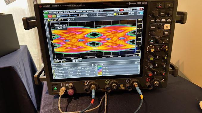
As part of their demonstration, ASMedia had a classic eye diagram display. The eye diagram demoed has a clear opening in the center, which is indicative of good signal integrity, as the larger the eye opening, the less distortion and noise in the signal. The horizontal width of the eye opening represents the time window in which the signal can be sampled correctly, so the relatively narrow horizontal spread of the eye opening suggests that there is minimal jitter, meaning the signal transitions are consistent and predictable. Finally, the vertical height of the eye opening indicates the signal amplitude and the rather tall eye opening suggests a higher signal-to-noise ratio (SNR), meaning that the signal is strong compared to any noise present.
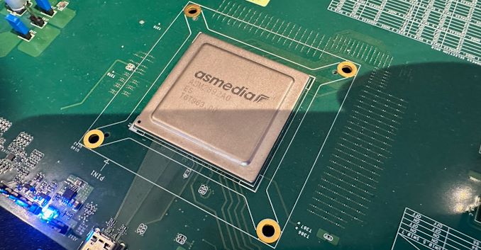
ASMedia itself is one of the major suppliers for discrete USB controllers, so the availability of ASMedia's USB4 v2 chip is crucial for adoption of the standard in general. While Intel will spearhead the industry with their Barlow Ridge Thunderbolt 5/USB4 v2 controller, ASMedia's controller is poised to end up in a far larger range of devices. So the importance of the company's USB4 v2 PHY demo is hard to overstate.
Demos aside, ASMedia is hoping to tape the chip out soon. If all goes well, the company expects their first USB4 v2 controllers to hit the market some time in the second half of 2025.

Lorem Ipsum is simply dummy text of the printing and typesetting industry. Lorem Ipsum has been the industry's.
G.Skill on Tuesday introduced its ultra-low-latency DDR5-6400 memory modules that feature a CAS latency of 30 clocks, which appears to be the industry's most aggressive timings yet for DDR5-6400 sticks. The modules will be available for both AMD and Intel CPU-based systems.
With every new generation of DDR memory comes an increase in data transfer rates and an extension of relative latencies. While for the vast majority of applications, the increased bandwidth offsets the performance impact of higher timings, there are applications that favor low latencies. However, shrinking latencies is sometimes harder than increasing data transfer rates, which is why low-latency modules are rare.
Nonetheless, G.Skill has apparently managed to cherry-pick enough DDR5 memory chips and build appropriate printed circuit boards to produce DDR5-6400 modules with CL30 timings, which are substantially lower than the CL46 timings recommended by JEDEC for this speed bin. This means that while JEDEC-standard modules have an absolute latency of 14.375 ns, G.Skill's modules can boast a latency of just 9.375 ns – an approximately 35% decrease.
G.Skill's DDR5-6400 CL30 39-39-102 modules have a capacity of 16 GB and will be available in 32 GB dual-channel kits, though the company does not disclose voltages, which are likely considerably higher than those standardized by JEDEC.
The company plans to make its DDR5-6400 modules available both for AMD systems with EXPO profiles (Trident Z5 Neo RGB and Trident Z5 Royal Neo) and for Intel-powered PCs with XMP 3.0 profiles (Trident Z5 RGB and Trident Z5 Royal). For AMD AM5 systems that have a practical limitation of 6000 MT/s – 6400 MT/s for DDR5 memory (as this is roughly as fast as AMD's Infinity Fabric can operate at with a 1:1 ratio), the new modules will be particularly beneficial for AMD's Ryzen 7000 and Ryzen 9000-series processors.
G.Skill notes that since its modules are non-standard, they will not work with all systems but will operate on high-end motherboards with properly cooled CPUs.
The new ultra-low-latency memory kits will be available worldwide from G.Skill's partners starting in late August 2024. The company did not disclose the pricing of these modules, but since we are talking about premium products that boast unique specifications, they are likely to be priced accordingly.
Memory


. Back at FMS 2022, the company had <a href="https://www.anandtech.com/show/17520/compute-express-link-cxl-30-announced-doubled-speeds-and-flexible-fabrics">announced</a> v3.0 of the CXL specifications. This was followed by CXL 3.1's <a href="https://www.businesswire.com/news/home/20231114332690/en/CXL-Consortium-Announces-Compute-Express-Link-3.1-Specification-Release">introduction</a> at Supercomputing 2023. Having started off as a host to device interconnect standard, it had slowly <a href="https://www.anandtech.com/show/17519/">subsumed other competing standards</a> such as OpenCAPI and Gen-Z. As a result, the specifications started to encompass a wide variety of use-cases by building a protocol on top of the the ubiquitous PCIe expansion bus. The CXL consortium comprises of heavyweights such as AMD and Intel, as well as a large number of startup companies attempting to play in different segments on the device side. At FMS 2024, CXL had a prime position in the booth demos of many vendors.</p>
<p align="center"><a href="https://www.anandtech.com/show/21533/cxl-gathers-momentum-at-fms-2024"><img alt="" src="https://images.anandtech.com/doci/21533/cxl-mem-hier_575px.jpg" /></a></p>
<p>The migration of server platforms from DDR4 to DDR5, along with the rise of workloads demanding large RAM capacity (but not particularly sensitive to either memory bandwidth or latency), has opened up memory expansion modules as one of the first set of widely available CXL devices. Over the last couple of years, we have had product announcements from <a href="https://www.anandtech.com/show/21333">Samsung</a> and <a href="https://www.anandtech.com/show/20003">Micron</a> in this area.</p>
<h3>SK hynix CMM-DDR5 CXL Memory Module and HMSDK</h3>
<p>At FMS 2024, SK hynix was showing off their DDR5-based CMM-DDR5 CXL memory module with a 128 GB capacity. The company was also detailing their associated Heterogeneous Memory Software Development Kit (HMSDK) - a set of libraries and tools at both the kernel and user levels aimed at increasing the ease of use of CXL memory. This is achieved in part by considering the memory pyramid / hierarchy and relocating the data between the server's main memory (DRAM) and the CXL device based on usage frequency.</p>
<p align="center"><a href="https://www.anandtech.com/show/21533/cxl-gathers-momentum-at-fms-2024"><img alt="" src="https://images.anandtech.com/doci/21533/skh-cmm-ddr5_575px.jpg" /></a></p>
<p>The CMM-DDR5 CXL memory module comes in the SDFF form-factor (E3.S 2T) with a PCIe 3.0 x8 host interface. The internal memory is based on 1α technology DRAM, and the device promises DDR5-class bandwidth and latency within a single NUMA hop. As these memory modules are meant to be used in datacenters and enterprises, the firmware includes features for RAS (reliability, availability, and serviceability) along with secure boot and other management features.</p>
<p>SK hynix was also demonstrating Niagara 2.0 - a hardware solution (currently based on FPGAs) to enable memory pooling and sharing - i.e, connecting multiple CXL memories to allow different hosts (CPUs and GPUs) to optimally share their capacity. The previous version only allowed capacity sharing, but the latest version enables sharing of data also. SK hynix had <a href="https://news.skhynix.com/sk-hynix-presents-ai-memory-solutions-at-cxl-devcon-2024/">presented</a> these solutions at the CXL DevCon 2024 earlier this year, but some progress seems to have been made in finalizing the specifications of the CMM-DDR5 at FMS 2024.</p>
<h3>Microchip and Micron Demonstrate CZ120 CXL Memory Expansion Module</h3>
<p>Micron had <a href="https://www.anandtech.com/show/20003/">unveiled</a> the CZ120 CXL Memory Expansion Module last year based on the Microchip SMC 2000 series CXL memory controller. At FMS 2024, Micron and Microchip had a demonstration of the module on a Granite Rapids server.</p>
<p align="center"><a href="https://www.anandtech.com/show/21533/cxl-gathers-momentum-at-fms-2024"><img alt="" src="https://images.anandtech.com/doci/21533/mchip-micron_575px.jpg" /></a></p>
<p>Additional insights into the SMC 2000 controller were also provided.</p>
<p align="center"><a href="https://www.anandtech.com/show/21533/cxl-gathers-momentum-at-fms-2024"><img alt="" src="https://images.anandtech.com/doci/21533/mchip-sm2000_575px.png" /></a></p>
<p>The CXL memory controller also incorporates DRAM die failure handling, and Microchip also provides diagnostics and debug tools to analyze failed modules. The memory controller also supports ECC, which forms part of the enterprise... Storage)
. Back at FMS 2022, the company had <a href="https://www.anandtech.com/show/17520/compute-express-link-cxl-30-announced-doubled-speeds-and-flexible-fabrics">announced</a> v3.0 of the CXL specifications. This was followed by CXL 3.1's <a href="https://www.businesswire.com/news/home/20231114332690/en/CXL-Consortium-Announces-Compute-Express-Link-3.1-Specification-Release">introduction</a> at Supercomputing 2023. Having started off as a host to device interconnect standard, it had slowly <a href="https://www.anandtech.com/show/17519/">subsumed other competing standards</a> such as OpenCAPI and Gen-Z. As a result, the specifications started to encompass a wide variety of use-cases by building a protocol on top of the the ubiquitous PCIe expansion bus. The CXL consortium comprises of heavyweights such as AMD and Intel, as well as a large number of startup companies attempting to play in different segments on the device side. At FMS 2024, CXL had a prime position in the booth demos of many vendors.</p>
<p align="center"><a href="https://www.anandtech.com/show/21533/cxl-gathers-momentum-at-fms-2024"><img alt="" src="https://images.anandtech.com/doci/21533/cxl-mem-hier_575px.jpg" /></a></p>
<p>The migration of server platforms from DDR4 to DDR5, along with the rise of workloads demanding large RAM capacity (but not particularly sensitive to either memory bandwidth or latency), has opened up memory expansion modules as one of the first set of widely available CXL devices. Over the last couple of years, we have had product announcements from <a href="https://www.anandtech.com/show/21333">Samsung</a> and <a href="https://www.anandtech.com/show/20003">Micron</a> in this area.</p>
<h3>SK hynix CMM-DDR5 CXL Memory Module and HMSDK</h3>
<p>At FMS 2024, SK hynix was showing off their DDR5-based CMM-DDR5 CXL memory module with a 128 GB capacity. The company was also detailing their associated Heterogeneous Memory Software Development Kit (HMSDK) - a set of libraries and tools at both the kernel and user levels aimed at increasing the ease of use of CXL memory. This is achieved in part by considering the memory pyramid / hierarchy and relocating the data between the server's main memory (DRAM) and the CXL device based on usage frequency.</p>
<p align="center"><a href="https://www.anandtech.com/show/21533/cxl-gathers-momentum-at-fms-2024"><img alt="" src="https://images.anandtech.com/doci/21533/skh-cmm-ddr5_575px.jpg" /></a></p>
<p>The CMM-DDR5 CXL memory module comes in the SDFF form-factor (E3.S 2T) with a PCIe 3.0 x8 host interface. The internal memory is based on 1α technology DRAM, and the device promises DDR5-class bandwidth and latency within a single NUMA hop. As these memory modules are meant to be used in datacenters and enterprises, the firmware includes features for RAS (reliability, availability, and serviceability) along with secure boot and other management features.</p>
<p>SK hynix was also demonstrating Niagara 2.0 - a hardware solution (currently based on FPGAs) to enable memory pooling and sharing - i.e, connecting multiple CXL memories to allow different hosts (CPUs and GPUs) to optimally share their capacity. The previous version only allowed capacity sharing, but the latest version enables sharing of data also. SK hynix had <a href="https://news.skhynix.com/sk-hynix-presents-ai-memory-solutions-at-cxl-devcon-2024/">presented</a> these solutions at the CXL DevCon 2024 earlier this year, but some progress seems to have been made in finalizing the specifications of the CMM-DDR5 at FMS 2024.</p>
<h3>Microchip and Micron Demonstrate CZ120 CXL Memory Expansion Module</h3>
<p>Micron had <a href="https://www.anandtech.com/show/20003/">unveiled</a> the CZ120 CXL Memory Expansion Module last year based on the Microchip SMC 2000 series CXL memory controller. At FMS 2024, Micron and Microchip had a demonstration of the module on a Granite Rapids server.</p>
<p align="center"><a href="https://www.anandtech.com/show/21533/cxl-gathers-momentum-at-fms-2024"><img alt="" src="https://images.anandtech.com/doci/21533/mchip-micron_575px.jpg" /></a></p>
<p>Additional insights into the SMC 2000 controller were also provided.</p>
<p align="center"><a href="https://www.anandtech.com/show/21533/cxl-gathers-momentum-at-fms-2024"><img alt="" src="https://images.anandtech.com/doci/21533/mchip-sm2000_575px.png" /></a></p>
<p>The CXL memory controller also incorporates DRAM die failure handling, and Microchip also provides diagnostics and debug tools to analyze failed modules. The memory controller also supports ECC, which forms part of the enterprise... Storage | https://compbuddey.blogspot.com/2025/02/cxl-gathers-momentum-at-fms-2024-cxl_17.html)
. Back at FMS 2022, the company had <a href="https://www.anandtech.com/show/17520/compute-express-link-cxl-30-announced-doubled-speeds-and-flexible-fabrics">announced</a> v3.0 of the CXL specifications. This was followed by CXL 3.1's <a href="https://www.businesswire.com/news/home/20231114332690/en/CXL-Consortium-Announces-Compute-Express-Link-3.1-Specification-Release">introduction</a> at Supercomputing 2023. Having started off as a host to device interconnect standard, it had slowly <a href="https://www.anandtech.com/show/17519/">subsumed other competing standards</a> such as OpenCAPI and Gen-Z. As a result, the specifications started to encompass a wide variety of use-cases by building a protocol on top of the the ubiquitous PCIe expansion bus. The CXL consortium comprises of heavyweights such as AMD and Intel, as well as a large number of startup companies attempting to play in different segments on the device side. At FMS 2024, CXL had a prime position in the booth demos of many vendors.</p>
<p align="center"><a href="https://www.anandtech.com/show/21533/cxl-gathers-momentum-at-fms-2024"><img alt="" src="https://images.anandtech.com/doci/21533/cxl-mem-hier_575px.jpg" /></a></p>
<p>The migration of server platforms from DDR4 to DDR5, along with the rise of workloads demanding large RAM capacity (but not particularly sensitive to either memory bandwidth or latency), has opened up memory expansion modules as one of the first set of widely available CXL devices. Over the last couple of years, we have had product announcements from <a href="https://www.anandtech.com/show/21333">Samsung</a> and <a href="https://www.anandtech.com/show/20003">Micron</a> in this area.</p>
<h3>SK hynix CMM-DDR5 CXL Memory Module and HMSDK</h3>
<p>At FMS 2024, SK hynix was showing off their DDR5-based CMM-DDR5 CXL memory module with a 128 GB capacity. The company was also detailing their associated Heterogeneous Memory Software Development Kit (HMSDK) - a set of libraries and tools at both the kernel and user levels aimed at increasing the ease of use of CXL memory. This is achieved in part by considering the memory pyramid / hierarchy and relocating the data between the server's main memory (DRAM) and the CXL device based on usage frequency.</p>
<p align="center"><a href="https://www.anandtech.com/show/21533/cxl-gathers-momentum-at-fms-2024"><img alt="" src="https://images.anandtech.com/doci/21533/skh-cmm-ddr5_575px.jpg" /></a></p>
<p>The CMM-DDR5 CXL memory module comes in the SDFF form-factor (E3.S 2T) with a PCIe 3.0 x8 host interface. The internal memory is based on 1α technology DRAM, and the device promises DDR5-class bandwidth and latency within a single NUMA hop. As these memory modules are meant to be used in datacenters and enterprises, the firmware includes features for RAS (reliability, availability, and serviceability) along with secure boot and other management features.</p>
<p>SK hynix was also demonstrating Niagara 2.0 - a hardware solution (currently based on FPGAs) to enable memory pooling and sharing - i.e, connecting multiple CXL memories to allow different hosts (CPUs and GPUs) to optimally share their capacity. The previous version only allowed capacity sharing, but the latest version enables sharing of data also. SK hynix had <a href="https://news.skhynix.com/sk-hynix-presents-ai-memory-solutions-at-cxl-devcon-2024/">presented</a> these solutions at the CXL DevCon 2024 earlier this year, but some progress seems to have been made in finalizing the specifications of the CMM-DDR5 at FMS 2024.</p>
<h3>Microchip and Micron Demonstrate CZ120 CXL Memory Expansion Module</h3>
<p>Micron had <a href="https://www.anandtech.com/show/20003/">unveiled</a> the CZ120 CXL Memory Expansion Module last year based on the Microchip SMC 2000 series CXL memory controller. At FMS 2024, Micron and Microchip had a demonstration of the module on a Granite Rapids server.</p>
<p align="center"><a href="https://www.anandtech.com/show/21533/cxl-gathers-momentum-at-fms-2024"><img alt="" src="https://images.anandtech.com/doci/21533/mchip-micron_575px.jpg" /></a></p>
<p>Additional insights into the SMC 2000 controller were also provided.</p>
<p align="center"><a href="https://www.anandtech.com/show/21533/cxl-gathers-momentum-at-fms-2024"><img alt="" src="https://images.anandtech.com/doci/21533/mchip-sm2000_575px.png" /></a></p>
<p>The CXL memory controller also incorporates DRAM die failure handling, and Microchip also provides diagnostics and debug tools to analyze failed modules. The memory controller also supports ECC, which forms part of the enterprise... Storage&body=https://compbuddey.blogspot.com/2025/02/cxl-gathers-momentum-at-fms-2024-cxl_17.html)
0 Comments