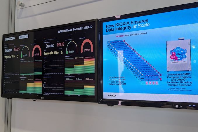

At FMS 2024, Kioxia had a proof-of-concept demonstration of their proposed a new RAID offload methodology for enterprise SSDs. The impetus for this is quite clear: as SSDs get faster in each generation, RAID arrays have a major problem of maintaining (and scaling up) performance. Even in cases where the RAID operations are handled by a dedicated RAID card, a simple write request in, say, a RAID 5 array would involve two reads and two writes to different drives. In cases where there is no hardware acceleration, the data from the reads needs to travel all the way back to the CPU and main memory for further processing before the writes can be done.
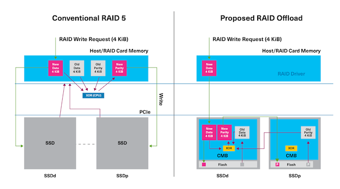
Kioxia has proposed the use of the PCIe direct memory access feature along with the SSD controller's controller memory buffer (CMB) to avoid the movement of data up to the CPU and back. The required parity computation is done by an accelerator block resident within the SSD controller.
In Kioxia's PoC implementation, the DMA engine can access the entire host address space (including the peer SSD's BAR-mapped CMB), allowing it to receive and transfer data as required from neighboring SSDs on the bus. Kioxia noted that their offload PoC saw close to 50% reduction in CPU utilization and upwards of 90% reduction in system DRAM utilization compared to software RAID done on the CPU. The proposed offload scheme can also handle scrubbing operations without taking up the host CPU cycles for the parity computation task.
Kioxia has already taken steps to contribute these features to the NVM Express working group. If accepted, the proposed offload scheme will be part of a standard that could become widely available across multiple SSD vendors.
Storage

Demand for high-performance processors for AI training is skyrocketing, and consequently so is the demand for the components that go into these processors. So much so that SK hynix this week is very publicly announcing that the company's high-bandwidth memory (HBM) production capacity has already sold out for the rest of 2024, and even most of 2025 has already sold out as well.
SK hynix currently produces various types of HBM memory for customers like Amazon, AMD, Facebook, Google (Broadcom), Intel, Microsoft, and, of course, NVIDIA. The latter is an especially prolific consumer of HBM3 and HBM3E memory for its H100/H200/GH200 accelerators, as NVIDIA is also working to fill what remains an insatiable (and unmet) demand for its accelerators.
As a result, HBM memory orders, which are already placed months in advance, are now backlogging well into 2025 as chip vendors look to secure supplies of the memory stacks critical to their success.
This has made SK hynix the secnd HBM memory vendor in recent months to announce that they've sold out into 2025, following an earlier announcement from Micron regarding its HBM3E production. But of the two announcements, SK hynix's is arguably the most significant yet, as the South Korean firm's HBM production capacity is far greater than Micron's. So while things were merely "interesting" with the smallest of the Big Three memory manufacturers being sold out into 2025, things are taking a more concerning (and constrained) outlook now that SK hynix is as well.
SK hynix currently controls roughly 46% - 49% of HBM market, and its share is not expected to drop significantly in 2025, according to market tracking firm TrendForce. By contrast, Micron's share on HBM memory market is between 4% and 6%. Since HBM supply of both companies is sold out through the most of 2025, we're likely looking at a scenario where over 50% of the industry's total HBM3/HBM3E supply for the coming quarters is already sold out.
This leaves Samsung as the only member of the group not to comment on HBM demand so far. Though with memory being a highly fungible commodity product, it would be surprising if Samsung wasn't facing similar demand. And, ultimately, all of this is pointing towards the indusry entering an HBM3 memory shortage.
Separately, SK hynix said that it is sampling 12-Hi 36GB HBM3E stacks with customers and will begin volume shipments in the third quarter.
Memory
Lorem Ipsum is simply dummy text of the printing and typesetting industry. Lorem Ipsum has been the industry's.
Demand for high-performance processors for AI training is skyrocketing, and consequently so is the demand for the components that go into these processors. So much so that SK hynix this week is very publicly announcing that the company's high-bandwidth memory (HBM) production capacity has already sold out for the rest of 2024, and even most of 2025 has already sold out as well.
SK hynix currently produces various types of HBM memory for customers like Amazon, AMD, Facebook, Google (Broadcom), Intel, Microsoft, and, of course, NVIDIA. The latter is an especially prolific consumer of HBM3 and HBM3E memory for its H100/H200/GH200 accelerators, as NVIDIA is also working to fill what remains an insatiable (and unmet) demand for its accelerators.
As a result, HBM memory orders, which are already placed months in advance, are now backlogging well into 2025 as chip vendors look to secure supplies of the memory stacks critical to their success.
This has made SK hynix the secnd HBM memory vendor in recent months to announce that they've sold out into 2025, following an earlier announcement from Micron regarding its HBM3E production. But of the two announcements, SK hynix's is arguably the most significant yet, as the South Korean firm's HBM production capacity is far greater than Micron's. So while things were merely "interesting" with the smallest of the Big Three memory manufacturers being sold out into 2025, things are taking a more concerning (and constrained) outlook now that SK hynix is as well.
SK hynix currently controls roughly 46% - 49% of HBM market, and its share is not expected to drop significantly in 2025, according to market tracking firm TrendForce. By contrast, Micron's share on HBM memory market is between 4% and 6%. Since HBM supply of both companies is sold out through the most of 2025, we're likely looking at a scenario where over 50% of the industry's total HBM3/HBM3E supply for the coming quarters is already sold out.
This leaves Samsung as the only member of the group not to comment on HBM demand so far. Though with memory being a highly fungible commodity product, it would be surprising if Samsung wasn't facing similar demand. And, ultimately, all of this is pointing towards the indusry entering an HBM3 memory shortage.
Separately, SK hynix said that it is sampling 12-Hi 36GB HBM3E stacks with customers and will begin volume shipments in the third quarter.
Memory


 performance. Even in cases where the RAID operations are handled by a dedicated RAID card, a simple write request in, say, a RAID 5 array would involve two reads and two writes to different drives. In cases where there is no hardware acceleration, the data from the reads needs to travel all the way back to the CPU and main memory for further processing before the writes can be done.</p>
<p align="center"><a href="https://www.anandtech.com/show/21523/kioxia-demonstrates-raid-offload-scheme-for-nvme-drives"><img alt="" src="https://images.anandtech.com/doci/21523/raidoff-mid_575px.png" /></a></p>
<p>Kioxia has proposed the use of the PCIe direct memory access feature along with the SSD controller's controller memory buffer (CMB) to avoid the movement of data up to the CPU and back. The required parity computation is done by an accelerator block resident within the SSD controller.</p>
<p>In Kioxia's PoC implementation, the DMA engine can access the entire host address space (including the peer SSD's BAR-mapped CMB), allowing it to receive and transfer data as required from neighboring SSDs on the bus. Kioxia noted that their offload PoC saw close to 50% reduction in CPU utilization and upwards of 90% reduction in system DRAM utilization compared to software RAID done on the CPU. The proposed offload scheme can also handle scrubbing operations without taking up the host CPU cycles for the parity computation task.</p>
<p>Kioxia has already taken steps to contribute these features to the NVM Express working group. If accepted, the proposed offload scheme will be part of a standard that could become widely available across multiple SSD vendors.</p>
</p> Storage)
 performance. Even in cases where the RAID operations are handled by a dedicated RAID card, a simple write request in, say, a RAID 5 array would involve two reads and two writes to different drives. In cases where there is no hardware acceleration, the data from the reads needs to travel all the way back to the CPU and main memory for further processing before the writes can be done.</p>
<p align="center"><a href="https://www.anandtech.com/show/21523/kioxia-demonstrates-raid-offload-scheme-for-nvme-drives"><img alt="" src="https://images.anandtech.com/doci/21523/raidoff-mid_575px.png" /></a></p>
<p>Kioxia has proposed the use of the PCIe direct memory access feature along with the SSD controller's controller memory buffer (CMB) to avoid the movement of data up to the CPU and back. The required parity computation is done by an accelerator block resident within the SSD controller.</p>
<p>In Kioxia's PoC implementation, the DMA engine can access the entire host address space (including the peer SSD's BAR-mapped CMB), allowing it to receive and transfer data as required from neighboring SSDs on the bus. Kioxia noted that their offload PoC saw close to 50% reduction in CPU utilization and upwards of 90% reduction in system DRAM utilization compared to software RAID done on the CPU. The proposed offload scheme can also handle scrubbing operations without taking up the host CPU cycles for the parity computation task.</p>
<p>Kioxia has already taken steps to contribute these features to the NVM Express working group. If accepted, the proposed offload scheme will be part of a standard that could become widely available across multiple SSD vendors.</p>
</p> Storage | https://compbuddey.blogspot.com/2025/01/kioxia-demonstrates-raid-offload-scheme_26.html)
 performance. Even in cases where the RAID operations are handled by a dedicated RAID card, a simple write request in, say, a RAID 5 array would involve two reads and two writes to different drives. In cases where there is no hardware acceleration, the data from the reads needs to travel all the way back to the CPU and main memory for further processing before the writes can be done.</p>
<p align="center"><a href="https://www.anandtech.com/show/21523/kioxia-demonstrates-raid-offload-scheme-for-nvme-drives"><img alt="" src="https://images.anandtech.com/doci/21523/raidoff-mid_575px.png" /></a></p>
<p>Kioxia has proposed the use of the PCIe direct memory access feature along with the SSD controller's controller memory buffer (CMB) to avoid the movement of data up to the CPU and back. The required parity computation is done by an accelerator block resident within the SSD controller.</p>
<p>In Kioxia's PoC implementation, the DMA engine can access the entire host address space (including the peer SSD's BAR-mapped CMB), allowing it to receive and transfer data as required from neighboring SSDs on the bus. Kioxia noted that their offload PoC saw close to 50% reduction in CPU utilization and upwards of 90% reduction in system DRAM utilization compared to software RAID done on the CPU. The proposed offload scheme can also handle scrubbing operations without taking up the host CPU cycles for the parity computation task.</p>
<p>Kioxia has already taken steps to contribute these features to the NVM Express working group. If accepted, the proposed offload scheme will be part of a standard that could become widely available across multiple SSD vendors.</p>
</p> Storage&body=https://compbuddey.blogspot.com/2025/01/kioxia-demonstrates-raid-offload-scheme_26.html)
0 Comments