
The CXL consortium has had a regular presence at FMS (which rechristened itself from 'Flash Memory Summit' to the 'Future of Memory and Storage' this year). Back at FMS 2022, the company had announced v3.0 of the CXL specifications. This was followed by CXL 3.1's introduction at Supercomputing 2023. Having started off as a host to device interconnect standard, it had slowly subsumed other competing standards such as OpenCAPI and Gen-Z. As a result, the specifications started to encompass a wide variety of use-cases by building a protocol on top of the the ubiquitous PCIe expansion bus. The CXL consortium comprises of heavyweights such as AMD and Intel, as well as a large number of startup companies attempting to play in different segments on the device side. At FMS 2024, CXL had a prime position in the booth demos of many vendors.
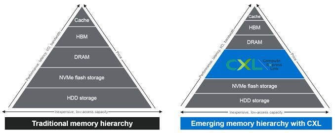
The migration of server platforms from DDR4 to DDR5, along with the rise of workloads demanding large RAM capacity (but not particularly sensitive to either memory bandwidth or latency), has opened up memory expansion modules as one of the first set of widely available CXL devices. Over the last couple of years, we have had product announcements from Samsung and Micron in this area.
At FMS 2024, SK hynix was showing off their DDR5-based CMM-DDR5 CXL memory module with a 128 GB capacity. The company was also detailing their associated Heterogeneous Memory Software Development Kit (HMSDK) - a set of libraries and tools at both the kernel and user levels aimed at increasing the ease of use of CXL memory. This is achieved in part by considering the memory pyramid / hierarchy and relocating the data between the server's main memory (DRAM) and the CXL device based on usage frequency.
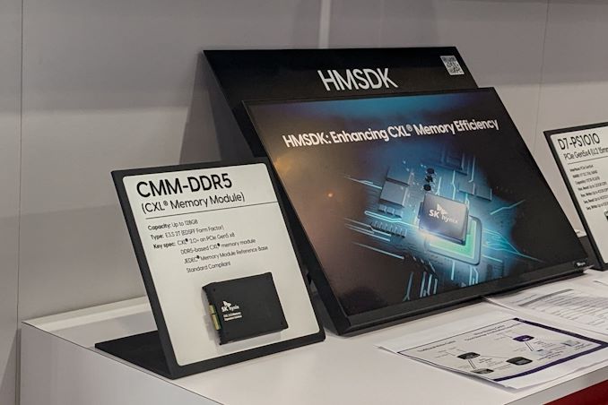
The CMM-DDR5 CXL memory module comes in the SDFF form-factor (E3.S 2T) with a PCIe 3.0 x8 host interface. The internal memory is based on 1α technology DRAM, and the device promises DDR5-class bandwidth and latency within a single NUMA hop. As these memory modules are meant to be used in datacenters and enterprises, the firmware includes features for RAS (reliability, availability, and serviceability) along with secure boot and other management features.
SK hynix was also demonstrating Niagara 2.0 - a hardware solution (currently based on FPGAs) to enable memory pooling and sharing - i.e, connecting multiple CXL memories to allow different hosts (CPUs and GPUs) to optimally share their capacity. The previous version only allowed capacity sharing, but the latest version enables sharing of data also. SK hynix had presented these solutions at the CXL DevCon 2024 earlier this year, but some progress seems to have been made in finalizing the specifications of the CMM-DDR5 at FMS 2024.
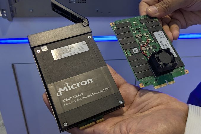
Micron had unveiled the CZ120 CXL Memory Expansion Module last year based on the Microchip SMC 2000 series CXL memory controller. At FMS 2024, Micron and Microchip had a demonstration of the module on a Granite Rapids server.
Additional insights into the SMC 2000 controller were also provided.
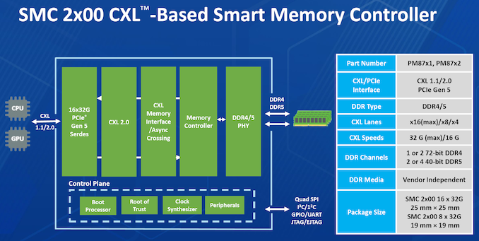
The CXL memory controller also incorporates DRAM die failure handling, and Microchip also provides diagnostics and debug tools to analyze failed modules. The memory controller also supports ECC, which forms part of the enterprise... Storage


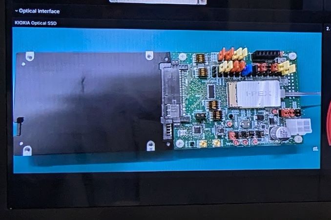
A few years back, the Japanese government's New Energy and Industrial Technology Development Organization (NEDO ) allocated funding for the development of green datacenter technologies. With the aim to obtain up to 40% savings in overall power consumption, several Japanese companies have been developing an optical interface for their enterprise SSDs. And at this year's FMS, Kioxia had their optical interface on display.
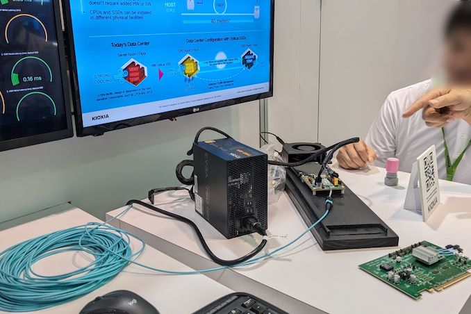
For this demonstration, Kioxia took its existing CM7 enterprise SSD and created an optical interface for it. A PCIe card with on-board optics developed by Kyocera is installed in the server slot. An optical interface allows data transfer over long distances (it was 40m in the demo, but Kioxia promises lengths of up to 100m for the cable in the future). This allows the storage to be kept in a separate room with minimal cooling requirements compared to the rack with the CPUs and GPUs. Disaggregation of different server components will become an option as very high throughput interfaces such as PCIe 7.0 (with 128 GT/s rates) become available.
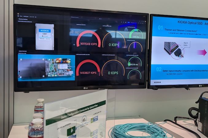
The demonstration of the optical SSD showed a slight loss in IOPS performance, but a significant advantage in the latency metric over the shipping enterprise SSD behind a copper network link. Obviously, there are advantages in wiring requirements and signal integrity maintenance with optical links.
Being a proof-of-concept demonstration, we do see the requirement for an industry-standard approach if this were to gain adoption among different datacenter vendors. The PCI-SIG optical workgroup will need to get its act together soon to create a standards-based approach to this problem.
Storage
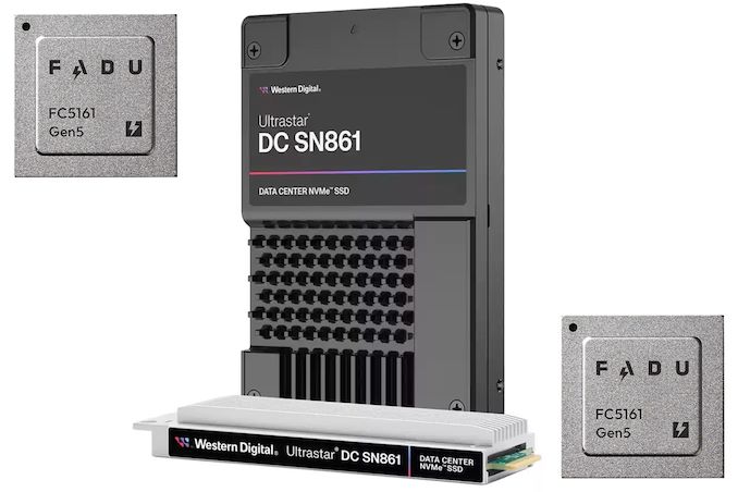
When Western Digital introduced its Ultrastar DC SN861 SSDs earlier this year, the company did not disclose which controller it used for these drives, which made many observers presume that WD was using an in-house controller. But a recent teardown of the drive shows that is not the case; instead, the company is using a controller from Fadu, a South Korean company founded in 2015 that specializes on enterprise-grade turnkey SSD solutions.
The Western Digital Ultrastar DC SN861 SSD is aimed at performance-hungry hyperscale datacenters and enterprise customers which are adopting PCIe Gen5 storage devices these days. And, as uncovered in photos from a recent Storage Review article, the drive is based on Fadu's FC5161 NVMe 2.0-compliant controller. The FC5161 utilizes 16 NAND channels supporting an ONFi 5.0 2400 MT/s interface, and features a combination of enterprise-grade capabilities (OCP Cloud Spec 2.0, SR-IOV, up to 512 name spaces for ZNS support, flexible data placement, NVMe-MI 1.2, advanced security, telemetry, power loss protection) not available on other off-the-shelf controllers – or on any previous Western Digital controllers.
The Ultrastar DC SN861 SSD offers sequential read speeds up to 13.7 GB/s as well as sequential write speeds up to 7.5 GB/s. As for random performance, it boasts with an up to 3.3 million random 4K read IOPS and up to 0.8 million random 4K write IOPS. The drives are available in capacities between 1.6 TB and 7.68 TB with one or three drive writes per day (DWPD) over five years rating as well as in U.2 and E1.S form-factors.
While the two form factors of the SN861 share a similar technical design, Western Digital has tailored each version for distinct workloads: the E1.S supports FDP and performance enhancements specifically for cloud environments. By contrast, the U.2 model is geared towards high-performance enterprise tasks and emerging applications like AI.
Without any doubts, Western Digital's Ultrastar DC SN861 is a feature-rich high-performance enterprise-grade SSD. It has another distinctive feature: a 5W idle power consumption, which is rather low by the standards of enterprise-grade drives (e.g., it is 1W lower compared to the SN840). While the difference with predecessors may be just 1W, hyperscalers deploy thousands of drives and for their TCO every watt counts.
Western Digital's Ultrastar DC SN861 SSDs are now available for purchase to select customers (such as Meta) and to interested parties. Prices are unknown, but they will depend on such factors as volumes.
Sources: Fadu, Storage Review
Storage
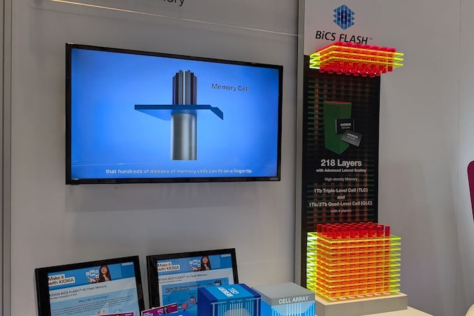
Kioxia's booth at FMS 2024 was a busy one with multiple technology demonstrations keeping visitors occupied. A walk-through of the BiCS 8 manufacturing process was the first to grab my attention. Kioxia and Western Digital announced the sampling of BiCS 8 in March 2023. We had touched briefly upon its CMOS Bonded Array (CBA) scheme in our coverage of Kioxial's 2Tb QLC NAND device and coverage of Western Digital's 128 TB QLC enterprise SSD proof-of-concept demonstration. At Kioxia's booth, we got more insights.
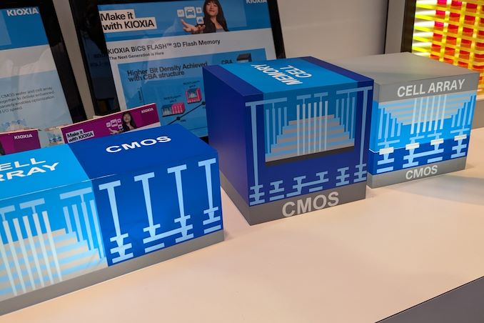
Traditionally, fabrication of flash chips involved placement of the associate logic circuitry (CMOS process) around the periphery of the flash array. The process then moved on to putting the CMOS under the cell array, but the wafer development process was serialized with the CMOS logic getting fabricated first followed by the cell array on top. However, this has some challenges because the cell array requires a high-temperature processing step to ensure higher reliability that can be detrimental to the health of the CMOS logic. Thanks to recent advancements in wafer bonding techniques, the new CBA process allows the CMOS wafer and cell array wafer to be processed independently in parallel and then pieced together, as shown in the models above.
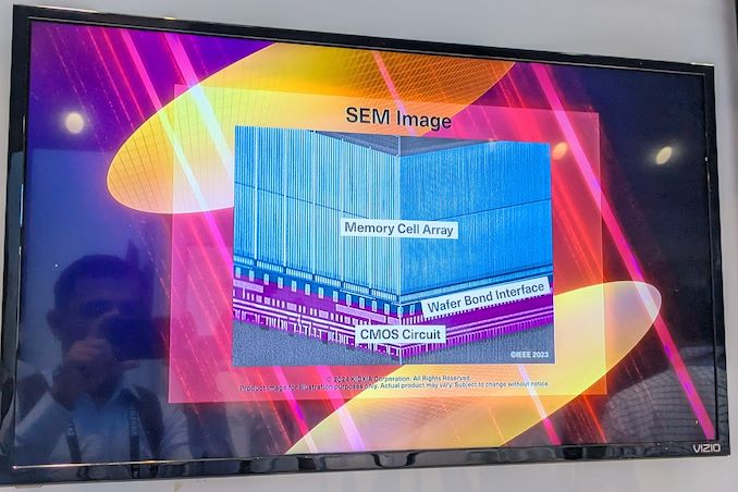
The BiCS 8 3D NAND incorporates 218 layers, compared to 112 layers in BiCS 5 and 162 layers in BiCS 6. The company decided to skip over BiCS 7 (or, rather, it was probably a short-lived generation meant as an internal test vehicle). The generation retains the four-plane charge trap structure of BiCS 6. In its TLC avatar, it is available as a 1 Tbit device. The QLC version is available in two capacities - 1 Tbit and 2 Tbit.
Kioxia also noted that while the number of layers (218) doesn't compare favorably with the latest layer counts from the competition, its lateral scaling / cell shrinkage has enabled it to be competitive in terms of bit density as well as operating speeds (3200 MT/s). For reference, the latest shipping NAND from Micron - the G9 - has 276 layers with a bit density in TLC mode of 21 Gbit/mm2, and operates at up to 3600 MT/s. However, its 232L NAND operates only up to 2400 MT/s and has a bit density of 14.6 Gbit/mm2.
It must be noted that the CBA hybrid bonding process has advantages over the current processes used by other vendors - including Micron's CMOS under array (CuA) and SK hynix's 4D PUC (periphery-under-chip) developed in the late 2010s. It is expected that other NAND vendors will also move eventually to some variant of the hybrid bonding scheme used by Kioxia.
Storage
A few years back, the Japanese government's New Energy and Industrial Technology Development Organization (NEDO ) allocated funding for the development of green datacenter technologies. With the aim to obtain up to 40% savings in overall power consumption, several Japanese companies have been developing an optical interface for their enterprise SSDs. And at this year's FMS, Kioxia had their optical interface on display.
For this demonstration, Kioxia took its existing CM7 enterprise SSD and created an optical interface for it. A PCIe card with on-board optics developed by Kyocera is installed in the server slot. An optical interface allows data transfer over long distances (it was 40m in the demo, but Kioxia promises lengths of up to 100m for the cable in the future). This allows the storage to be kept in a separate room with minimal cooling requirements compared to the rack with the CPUs and GPUs. Disaggregation of different server components will become an option as very high throughput interfaces such as PCIe 7.0 (with 128 GT/s rates) become available.
The demonstration of the optical SSD showed a slight loss in IOPS performance, but a significant advantage in the latency metric over the shipping enterprise SSD behind a copper network link. Obviously, there are advantages in wiring requirements and signal integrity maintenance with optical links.
Being a proof-of-concept demonstration, we do see the requirement for an industry-standard approach if this were to gain adoption among different datacenter vendors. The PCI-SIG optical workgroup will need to get its act together soon to create a standards-based approach to this problem.
Storage
When Western Digital introduced its Ultrastar DC SN861 SSDs earlier this year, the company did not disclose which controller it used for these drives, which made many observers presume that WD was using an in-house controller. But a recent teardown of the drive shows that is not the case; instead, the company is using a controller from Fadu, a South Korean company founded in 2015 that specializes on enterprise-grade turnkey SSD solutions.
The Western Digital Ultrastar DC SN861 SSD is aimed at performance-hungry hyperscale datacenters and enterprise customers which are adopting PCIe Gen5 storage devices these days. And, as uncovered in photos from a recent Storage Review article, the drive is based on Fadu's FC5161 NVMe 2.0-compliant controller. The FC5161 utilizes 16 NAND channels supporting an ONFi 5.0 2400 MT/s interface, and features a combination of enterprise-grade capabilities (OCP Cloud Spec 2.0, SR-IOV, up to 512 name spaces for ZNS support, flexible data placement, NVMe-MI 1.2, advanced security, telemetry, power loss protection) not available on other off-the-shelf controllers – or on any previous Western Digital controllers.
The Ultrastar DC SN861 SSD offers sequential read speeds up to 13.7 GB/s as well as sequential write speeds up to 7.5 GB/s. As for random performance, it boasts with an up to 3.3 million random 4K read IOPS and up to 0.8 million random 4K write IOPS. The drives are available in capacities between 1.6 TB and 7.68 TB with one or three drive writes per day (DWPD) over five years rating as well as in U.2 and E1.S form-factors.
While the two form factors of the SN861 share a similar technical design, Western Digital has tailored each version for distinct workloads: the E1.S supports FDP and performance enhancements specifically for cloud environments. By contrast, the U.2 model is geared towards high-performance enterprise tasks and emerging applications like AI.
Without any doubts, Western Digital's Ultrastar DC SN861 is a feature-rich high-performance enterprise-grade SSD. It has another distinctive feature: a 5W idle power consumption, which is rather low by the standards of enterprise-grade drives (e.g., it is 1W lower compared to the SN840). While the difference with predecessors may be just 1W, hyperscalers deploy thousands of drives and for their TCO every watt counts.
Western Digital's Ultrastar DC SN861 SSDs are now available for purchase to select customers (such as Meta) and to interested parties. Prices are unknown, but they will depend on such factors as volumes.
Sources: Fadu, Storage Review
Storage
Kioxia's booth at FMS 2024 was a busy one with multiple technology demonstrations keeping visitors occupied. A walk-through of the BiCS 8 manufacturing process was the first to grab my attention. Kioxia and Western Digital announced the sampling of BiCS 8 in March 2023. We had touched briefly upon its CMOS Bonded Array (CBA) scheme in our coverage of Kioxial's 2Tb QLC NAND device and coverage of Western Digital's 128 TB QLC enterprise SSD proof-of-concept demonstration. At Kioxia's booth, we got more insights.
Traditionally, fabrication of flash chips involved placement of the associate logic circuitry (CMOS process) around the periphery of the flash array. The process then moved on to putting the CMOS under the cell array, but the wafer development process was serialized with the CMOS logic getting fabricated first followed by the cell array on top. However, this has some challenges because the cell array requires a high-temperature processing step to ensure higher reliability that can be detrimental to the health of the CMOS logic. Thanks to recent advancements in wafer bonding techniques, the new CBA process allows the CMOS wafer and cell array wafer to be processed independently in parallel and then pieced together, as shown in the models above.
The BiCS 8 3D NAND incorporates 218 layers, compared to 112 layers in BiCS 5 and 162 layers in BiCS 6. The company decided to skip over BiCS 7 (or, rather, it was probably a short-lived generation meant as an internal test vehicle). The generation retains the four-plane charge trap structure of BiCS 6. In its TLC avatar, it is available as a 1 Tbit device. The QLC version is available in two capacities - 1 Tbit and 2 Tbit.
Kioxia also noted that while the number of layers (218) doesn't compare favorably with the latest layer counts from the competition, its lateral scaling / cell shrinkage has enabled it to be competitive in terms of bit density as well as operating speeds (3200 MT/s). For reference, the latest shipping NAND from Micron - the G9 - has 276 layers with a bit density in TLC mode of 21 Gbit/mm2, and operates at up to 3600 MT/s. However, its 232L NAND operates only up to 2400 MT/s and has a bit density of 14.6 Gbit/mm2.
It must be noted that the CBA hybrid bonding process has advantages over the current processes used by other vendors - including Micron's CMOS under array (CuA) and SK hynix's 4D PUC (periphery-under-chip) developed in the late 2010s. It is expected that other NAND vendors will also move eventually to some variant of the hybrid bonding scheme used by Kioxia.
Storage
It is with great sadness that I find myself penning the hardest news post I’ve ever needed to write here at AnandTech. After over 27 years of covering the wide – and wild – world of computing hardware, today is AnandTech’s final day of publication.
For better or worse, we’ve reached the end of a long journey – one that started with a review of an AMD processor, and has ended with the review of an AMD processor. It’s fittingly poetic, but it is also a testament to the fact that we’ve spent the last 27 years doing what we love, covering the chips that are the lifeblood of the computing industry.
A lot of things have changed in the last quarter-century – in 1997 NVIDIA had yet to even coin the term “GPU” – and we’ve been fortunate to watch the world of hardware continue to evolve over the time period. We’ve gone from boxy desktop computers and laptops that today we’d charitably classify as portable desktops, to pocket computers where even the cheapest budget device puts the fastest PC of 1997 to shame.
The years have also brought some monumental changes to the world of publishing. AnandTech was hardly the first hardware enthusiast website, nor will we be the last. But we were fortunate to thrive in the past couple of decades, when so many of our peers did not, thanks to a combination of hard work, strategic investments in people and products, even more hard work, and the support of our many friends, colleagues, and readers.
Still, few things last forever, and the market for written tech journalism is not what it once was – nor will it ever be again. So, the time has come for AnandTech to wrap up its work, and let the next generation of tech journalists take their place within the zeitgeist.
It has been my immense privilege to write for AnandTech for the past 19 years – and to manage it as its editor-in-chief for the past decade. And while I carry more than a bit of remorse in being AnandTech’s final boss, I can at least take pride in everything we’ve accomplished over the years, whether it’s lauding some legendary products, writing technology primers that still remain relevant today, or watching new stars rise in expected places. There is still more that I had wanted AnandTech to do, but after 21,500 articles, this was a good start.
And while the AnandTech staff is riding off into the sunset, I am happy to report that the site itself won’t be going anywhere for a while. Our publisher, Future PLC, will be keeping the AnandTech website and its many articles live indefinitely. So that all of the content we’ve created over the years remains accessible and citable. Even without new articles to add to the collection, I expect that many of the things we’ve written over the past couple of decades will remain relevant for years to come – and remain accessible just as long.
The AnandTech Forums will also continue to be operated by Future’s community team and our dedicated troop of moderators. With forum threads going back to 1999 (and some active members just as long), the forums have a history almost as long and as storied as AnandTech itself (wounded monitor children, anyone?). So even when AnandTech is no longer publishing articles, we’ll still have a place for everyone to talk about the latest in technology – and have those discussions last longer than 48 hours.
Finally, for everyone who still needs their technical writing fix, our formidable opposition of the last 27 years and fellow Future brand, Tom’s Hardware, is continuing to cover the world of technology. There are a couple of familiar AnandTech faces already over there providing their accumulated expertise, and the site will continue doing its best to provide a written take on technology news.
As I look back on everything AnandTech has accomplished over the past 27 years, there are more than a few people, groups, and companies that I would like to thank on behalf of both myself and AnandTech as a whole.
First and foremost, I cannot thank enough all the editors who have worked for AnandTech over the years. T... Site Updates
A few years back, the Japanese government's New Energy and Industrial Technology Development Organization (NEDO ) allocated funding for the development of green datacenter technologies. With the aim to obtain up to 40% savings in overall power consumption, several Japanese companies have been developing an optical interface for their enterprise SSDs. And at this year's FMS, Kioxia had their optical interface on display.
For this demonstration, Kioxia took its existing CM7 enterprise SSD and created an optical interface for it. A PCIe card with on-board optics developed by Kyocera is installed in the server slot. An optical interface allows data transfer over long distances (it was 40m in the demo, but Kioxia promises lengths of up to 100m for the cable in the future). This allows the storage to be kept in a separate room with minimal cooling requirements compared to the rack with the CPUs and GPUs. Disaggregation of different server components will become an option as very high throughput interfaces such as PCIe 7.0 (with 128 GT/s rates) become available.
The demonstration of the optical SSD showed a slight loss in IOPS performance, but a significant advantage in the latency metric over the shipping enterprise SSD behind a copper network link. Obviously, there are advantages in wiring requirements and signal integrity maintenance with optical links.
Being a proof-of-concept demonstration, we do see the requirement for an industry-standard approach if this were to gain adoption among different datacenter vendors. The PCI-SIG optical workgroup will need to get its act together soon to create a standards-based approach to this problem.
Storage
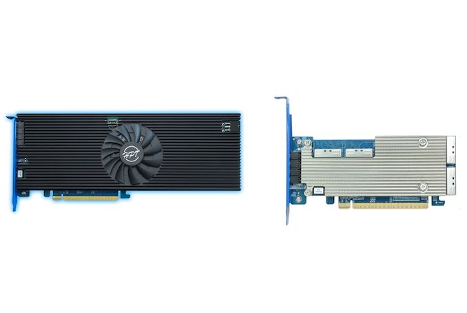
HighPoint Technologies has updated their NVMe switch and RAID solutions with PCIe 5.0, and supporting up to eight NVMe drives. The new HighPoint Rocket 1600 (switch add-in card) and 7600 series (RAID adapters) are the successors to the SSD SSD7500 series adapter cards introduced in 2020. Similar to its predecessors, the new Rocket series cards are also based on a Broadcom PCIe switch (PEX 89048). The Rocket 7600 series runs the RAID stack on the integrated ARM processor (dual-core Cortex A15)
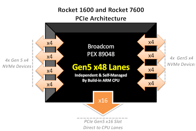
The PEX 89048 supports up to 48 PCIe 5.0 lanes, out of which 16 are dedicated to the host connection in the Rocket adapters. The use of a true PCIe switch means that the product doesn't rely on PCIe lane bifurcation support in the host platform.
HighPoint's Gen 5 stack currently has two products each in the switch and RAID lineups - an add-in card with support for M.2 drives, and a RAID adapter with four 5.0 x8 SFF-TA-1016 (Mini Cool Edge IO or MCIO) connectors for use with backplanes / setups involving U.2 / U.3 / EDSFF drives.
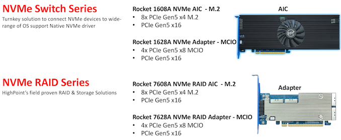
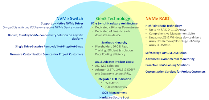
The RAID adapters require HighPoint's drivers (available for Linux, macOS, and Windows), and supports RAID 0, RAID 1, and RAID 10 arrays. On the other hand, the AIC requires no custom drivers. RAID configurations with the AIC will need to be handled by software running on the host OS. On the hardware side, all members of the Rocket series come with an external power connector (as the solution can consume upwards of 75W) and integrate a heatsink. The M.2 version is actively cooled, as the drives are housed within the full-height / full-length cards.
The solution can theoretically support up to 64 GBps of throughput, but real-world performance is limited to around 56 GBps using Gen 5 drives. It must be noted that even Gen 4 drives can take advantage of the new platform and deliver better performance with the new Rocket series compared to the older SSD7500 series.
The cards are shipping now, with pricing ranging from $1500 (add-in card) to $2000 (RAID adapters). HighPoint is not alone in targeting this HEDT / workstation market. Sabrent has been teasing their Apex Gen 5.0 x16 solution involving eight M.2 SSDs for a few months now (involving a Microchip PCIe switch. Until that solution comes to the market, HighPoint appears to be the only game in town for workstation users requiring access to direct-attached storage capable of delivering 50 GBps+ speeds.
SSDs
Lorem Ipsum is simply dummy text of the printing and typesetting industry. Lorem Ipsum has been the industry's.
A few years back, the Japanese government's New Energy and Industrial Technology Development Organization (NEDO ) allocated funding for the development of green datacenter technologies. With the aim to obtain up to 40% savings in overall power consumption, several Japanese companies have been developing an optical interface for their enterprise SSDs. And at this year's FMS, Kioxia had their optical interface on display.
For this demonstration, Kioxia took its existing CM7 enterprise SSD and created an optical interface for it. A PCIe card with on-board optics developed by Kyocera is installed in the server slot. An optical interface allows data transfer over long distances (it was 40m in the demo, but Kioxia promises lengths of up to 100m for the cable in the future). This allows the storage to be kept in a separate room with minimal cooling requirements compared to the rack with the CPUs and GPUs. Disaggregation of different server components will become an option as very high throughput interfaces such as PCIe 7.0 (with 128 GT/s rates) become available.
The demonstration of the optical SSD showed a slight loss in IOPS performance, but a significant advantage in the latency metric over the shipping enterprise SSD behind a copper network link. Obviously, there are advantages in wiring requirements and signal integrity maintenance with optical links.
Being a proof-of-concept demonstration, we do see the requirement for an industry-standard approach if this were to gain adoption among different datacenter vendors. The PCI-SIG optical workgroup will need to get its act together soon to create a standards-based approach to this problem.
Storage
When Western Digital introduced its Ultrastar DC SN861 SSDs earlier this year, the company did not disclose which controller it used for these drives, which made many observers presume that WD was using an in-house controller. But a recent teardown of the drive shows that is not the case; instead, the company is using a controller from Fadu, a South Korean company founded in 2015 that specializes on enterprise-grade turnkey SSD solutions.
The Western Digital Ultrastar DC SN861 SSD is aimed at performance-hungry hyperscale datacenters and enterprise customers which are adopting PCIe Gen5 storage devices these days. And, as uncovered in photos from a recent Storage Review article, the drive is based on Fadu's FC5161 NVMe 2.0-compliant controller. The FC5161 utilizes 16 NAND channels supporting an ONFi 5.0 2400 MT/s interface, and features a combination of enterprise-grade capabilities (OCP Cloud Spec 2.0, SR-IOV, up to 512 name spaces for ZNS support, flexible data placement, NVMe-MI 1.2, advanced security, telemetry, power loss protection) not available on other off-the-shelf controllers – or on any previous Western Digital controllers.
The Ultrastar DC SN861 SSD offers sequential read speeds up to 13.7 GB/s as well as sequential write speeds up to 7.5 GB/s. As for random performance, it boasts with an up to 3.3 million random 4K read IOPS and up to 0.8 million random 4K write IOPS. The drives are available in capacities between 1.6 TB and 7.68 TB with one or three drive writes per day (DWPD) over five years rating as well as in U.2 and E1.S form-factors.
While the two form factors of the SN861 share a similar technical design, Western Digital has tailored each version for distinct workloads: the E1.S supports FDP and performance enhancements specifically for cloud environments. By contrast, the U.2 model is geared towards high-performance enterprise tasks and emerging applications like AI.
Without any doubts, Western Digital's Ultrastar DC SN861 is a feature-rich high-performance enterprise-grade SSD. It has another distinctive feature: a 5W idle power consumption, which is rather low by the standards of enterprise-grade drives (e.g., it is 1W lower compared to the SN840). While the difference with predecessors may be just 1W, hyperscalers deploy thousands of drives and for their TCO every watt counts.
Western Digital's Ultrastar DC SN861 SSDs are now available for purchase to select customers (such as Meta) and to interested parties. Prices are unknown, but they will depend on such factors as volumes.
Sources: Fadu, Storage Review
Storage
. Back at FMS 2022, the company had <a href="https://www.anandtech.com/show/17520/compute-express-link-cxl-30-announced-doubled-speeds-and-flexible-fabrics">announced</a> v3.0 of the CXL specifications. This was followed by CXL 3.1's <a href="https://www.businesswire.com/news/home/20231114332690/en/CXL-Consortium-Announces-Compute-Express-Link-3.1-Specification-Release">introduction</a> at Supercomputing 2023. Having started off as a host to device interconnect standard, it had slowly <a href="https://www.anandtech.com/show/17519/">subsumed other competing standards</a> such as OpenCAPI and Gen-Z. As a result, the specifications started to encompass a wide variety of use-cases by building a protocol on top of the the ubiquitous PCIe expansion bus. The CXL consortium comprises of heavyweights such as AMD and Intel, as well as a large number of startup companies attempting to play in different segments on the device side. At FMS 2024, CXL had a prime position in the booth demos of many vendors.</p>
<p align="center"><a href="https://www.anandtech.com/show/21533/cxl-gathers-momentum-at-fms-2024"><img alt="" src="https://images.anandtech.com/doci/21533/cxl-mem-hier_575px.jpg" /></a></p>
<p>The migration of server platforms from DDR4 to DDR5, along with the rise of workloads demanding large RAM capacity (but not particularly sensitive to either memory bandwidth or latency), has opened up memory expansion modules as one of the first set of widely available CXL devices. Over the last couple of years, we have had product announcements from <a href="https://www.anandtech.com/show/21333">Samsung</a> and <a href="https://www.anandtech.com/show/20003">Micron</a> in this area.</p>
<h3>SK hynix CMM-DDR5 CXL Memory Module and HMSDK</h3>
<p>At FMS 2024, SK hynix was showing off their DDR5-based CMM-DDR5 CXL memory module with a 128 GB capacity. The company was also detailing their associated Heterogeneous Memory Software Development Kit (HMSDK) - a set of libraries and tools at both the kernel and user levels aimed at increasing the ease of use of CXL memory. This is achieved in part by considering the memory pyramid / hierarchy and relocating the data between the server's main memory (DRAM) and the CXL device based on usage frequency.</p>
<p align="center"><a href="https://www.anandtech.com/show/21533/cxl-gathers-momentum-at-fms-2024"><img alt="" src="https://images.anandtech.com/doci/21533/skh-cmm-ddr5_575px.jpg" /></a></p>
<p>The CMM-DDR5 CXL memory module comes in the SDFF form-factor (E3.S 2T) with a PCIe 3.0 x8 host interface. The internal memory is based on 1α technology DRAM, and the device promises DDR5-class bandwidth and latency within a single NUMA hop. As these memory modules are meant to be used in datacenters and enterprises, the firmware includes features for RAS (reliability, availability, and serviceability) along with secure boot and other management features.</p>
<p>SK hynix was also demonstrating Niagara 2.0 - a hardware solution (currently based on FPGAs) to enable memory pooling and sharing - i.e, connecting multiple CXL memories to allow different hosts (CPUs and GPUs) to optimally share their capacity. The previous version only allowed capacity sharing, but the latest version enables sharing of data also. SK hynix had <a href="https://news.skhynix.com/sk-hynix-presents-ai-memory-solutions-at-cxl-devcon-2024/">presented</a> these solutions at the CXL DevCon 2024 earlier this year, but some progress seems to have been made in finalizing the specifications of the CMM-DDR5 at FMS 2024.</p>
<h3>Microchip and Micron Demonstrate CZ120 CXL Memory Expansion Module</h3>
<p>Micron had <a href="https://www.anandtech.com/show/20003/">unveiled</a> the CZ120 CXL Memory Expansion Module last year based on the Microchip SMC 2000 series CXL memory controller. At FMS 2024, Micron and Microchip had a demonstration of the module on a Granite Rapids server.</p>
<p align="center"><a href="https://www.anandtech.com/show/21533/cxl-gathers-momentum-at-fms-2024"><img alt="" src="https://images.anandtech.com/doci/21533/mchip-micron_575px.jpg" /></a></p>
<p>Additional insights into the SMC 2000 controller were also provided.</p>
<p align="center"><a href="https://www.anandtech.com/show/21533/cxl-gathers-momentum-at-fms-2024"><img alt="" src="https://images.anandtech.com/doci/21533/mchip-sm2000_575px.png" /></a></p>
<p>The CXL memory controller also incorporates DRAM die failure handling, and Microchip also provides diagnostics and debug tools to analyze failed modules. The memory controller also supports ECC, which forms part of the enterprise... Storage)
. Back at FMS 2022, the company had <a href="https://www.anandtech.com/show/17520/compute-express-link-cxl-30-announced-doubled-speeds-and-flexible-fabrics">announced</a> v3.0 of the CXL specifications. This was followed by CXL 3.1's <a href="https://www.businesswire.com/news/home/20231114332690/en/CXL-Consortium-Announces-Compute-Express-Link-3.1-Specification-Release">introduction</a> at Supercomputing 2023. Having started off as a host to device interconnect standard, it had slowly <a href="https://www.anandtech.com/show/17519/">subsumed other competing standards</a> such as OpenCAPI and Gen-Z. As a result, the specifications started to encompass a wide variety of use-cases by building a protocol on top of the the ubiquitous PCIe expansion bus. The CXL consortium comprises of heavyweights such as AMD and Intel, as well as a large number of startup companies attempting to play in different segments on the device side. At FMS 2024, CXL had a prime position in the booth demos of many vendors.</p>
<p align="center"><a href="https://www.anandtech.com/show/21533/cxl-gathers-momentum-at-fms-2024"><img alt="" src="https://images.anandtech.com/doci/21533/cxl-mem-hier_575px.jpg" /></a></p>
<p>The migration of server platforms from DDR4 to DDR5, along with the rise of workloads demanding large RAM capacity (but not particularly sensitive to either memory bandwidth or latency), has opened up memory expansion modules as one of the first set of widely available CXL devices. Over the last couple of years, we have had product announcements from <a href="https://www.anandtech.com/show/21333">Samsung</a> and <a href="https://www.anandtech.com/show/20003">Micron</a> in this area.</p>
<h3>SK hynix CMM-DDR5 CXL Memory Module and HMSDK</h3>
<p>At FMS 2024, SK hynix was showing off their DDR5-based CMM-DDR5 CXL memory module with a 128 GB capacity. The company was also detailing their associated Heterogeneous Memory Software Development Kit (HMSDK) - a set of libraries and tools at both the kernel and user levels aimed at increasing the ease of use of CXL memory. This is achieved in part by considering the memory pyramid / hierarchy and relocating the data between the server's main memory (DRAM) and the CXL device based on usage frequency.</p>
<p align="center"><a href="https://www.anandtech.com/show/21533/cxl-gathers-momentum-at-fms-2024"><img alt="" src="https://images.anandtech.com/doci/21533/skh-cmm-ddr5_575px.jpg" /></a></p>
<p>The CMM-DDR5 CXL memory module comes in the SDFF form-factor (E3.S 2T) with a PCIe 3.0 x8 host interface. The internal memory is based on 1α technology DRAM, and the device promises DDR5-class bandwidth and latency within a single NUMA hop. As these memory modules are meant to be used in datacenters and enterprises, the firmware includes features for RAS (reliability, availability, and serviceability) along with secure boot and other management features.</p>
<p>SK hynix was also demonstrating Niagara 2.0 - a hardware solution (currently based on FPGAs) to enable memory pooling and sharing - i.e, connecting multiple CXL memories to allow different hosts (CPUs and GPUs) to optimally share their capacity. The previous version only allowed capacity sharing, but the latest version enables sharing of data also. SK hynix had <a href="https://news.skhynix.com/sk-hynix-presents-ai-memory-solutions-at-cxl-devcon-2024/">presented</a> these solutions at the CXL DevCon 2024 earlier this year, but some progress seems to have been made in finalizing the specifications of the CMM-DDR5 at FMS 2024.</p>
<h3>Microchip and Micron Demonstrate CZ120 CXL Memory Expansion Module</h3>
<p>Micron had <a href="https://www.anandtech.com/show/20003/">unveiled</a> the CZ120 CXL Memory Expansion Module last year based on the Microchip SMC 2000 series CXL memory controller. At FMS 2024, Micron and Microchip had a demonstration of the module on a Granite Rapids server.</p>
<p align="center"><a href="https://www.anandtech.com/show/21533/cxl-gathers-momentum-at-fms-2024"><img alt="" src="https://images.anandtech.com/doci/21533/mchip-micron_575px.jpg" /></a></p>
<p>Additional insights into the SMC 2000 controller were also provided.</p>
<p align="center"><a href="https://www.anandtech.com/show/21533/cxl-gathers-momentum-at-fms-2024"><img alt="" src="https://images.anandtech.com/doci/21533/mchip-sm2000_575px.png" /></a></p>
<p>The CXL memory controller also incorporates DRAM die failure handling, and Microchip also provides diagnostics and debug tools to analyze failed modules. The memory controller also supports ECC, which forms part of the enterprise... Storage)
. Back at FMS 2022, the company had <a href="https://www.anandtech.com/show/17520/compute-express-link-cxl-30-announced-doubled-speeds-and-flexible-fabrics">announced</a> v3.0 of the CXL specifications. This was followed by CXL 3.1's <a href="https://www.businesswire.com/news/home/20231114332690/en/CXL-Consortium-Announces-Compute-Express-Link-3.1-Specification-Release">introduction</a> at Supercomputing 2023. Having started off as a host to device interconnect standard, it had slowly <a href="https://www.anandtech.com/show/17519/">subsumed other competing standards</a> such as OpenCAPI and Gen-Z. As a result, the specifications started to encompass a wide variety of use-cases by building a protocol on top of the the ubiquitous PCIe expansion bus. The CXL consortium comprises of heavyweights such as AMD and Intel, as well as a large number of startup companies attempting to play in different segments on the device side. At FMS 2024, CXL had a prime position in the booth demos of many vendors.</p>
<p align="center"><a href="https://www.anandtech.com/show/21533/cxl-gathers-momentum-at-fms-2024"><img alt="" src="https://images.anandtech.com/doci/21533/cxl-mem-hier_575px.jpg" /></a></p>
<p>The migration of server platforms from DDR4 to DDR5, along with the rise of workloads demanding large RAM capacity (but not particularly sensitive to either memory bandwidth or latency), has opened up memory expansion modules as one of the first set of widely available CXL devices. Over the last couple of years, we have had product announcements from <a href="https://www.anandtech.com/show/21333">Samsung</a> and <a href="https://www.anandtech.com/show/20003">Micron</a> in this area.</p>
<h3>SK hynix CMM-DDR5 CXL Memory Module and HMSDK</h3>
<p>At FMS 2024, SK hynix was showing off their DDR5-based CMM-DDR5 CXL memory module with a 128 GB capacity. The company was also detailing their associated Heterogeneous Memory Software Development Kit (HMSDK) - a set of libraries and tools at both the kernel and user levels aimed at increasing the ease of use of CXL memory. This is achieved in part by considering the memory pyramid / hierarchy and relocating the data between the server's main memory (DRAM) and the CXL device based on usage frequency.</p>
<p align="center"><a href="https://www.anandtech.com/show/21533/cxl-gathers-momentum-at-fms-2024"><img alt="" src="https://images.anandtech.com/doci/21533/skh-cmm-ddr5_575px.jpg" /></a></p>
<p>The CMM-DDR5 CXL memory module comes in the SDFF form-factor (E3.S 2T) with a PCIe 3.0 x8 host interface. The internal memory is based on 1α technology DRAM, and the device promises DDR5-class bandwidth and latency within a single NUMA hop. As these memory modules are meant to be used in datacenters and enterprises, the firmware includes features for RAS (reliability, availability, and serviceability) along with secure boot and other management features.</p>
<p>SK hynix was also demonstrating Niagara 2.0 - a hardware solution (currently based on FPGAs) to enable memory pooling and sharing - i.e, connecting multiple CXL memories to allow different hosts (CPUs and GPUs) to optimally share their capacity. The previous version only allowed capacity sharing, but the latest version enables sharing of data also. SK hynix had <a href="https://news.skhynix.com/sk-hynix-presents-ai-memory-solutions-at-cxl-devcon-2024/">presented</a> these solutions at the CXL DevCon 2024 earlier this year, but some progress seems to have been made in finalizing the specifications of the CMM-DDR5 at FMS 2024.</p>
<h3>Microchip and Micron Demonstrate CZ120 CXL Memory Expansion Module</h3>
<p>Micron had <a href="https://www.anandtech.com/show/20003/">unveiled</a> the CZ120 CXL Memory Expansion Module last year based on the Microchip SMC 2000 series CXL memory controller. At FMS 2024, Micron and Microchip had a demonstration of the module on a Granite Rapids server.</p>
<p align="center"><a href="https://www.anandtech.com/show/21533/cxl-gathers-momentum-at-fms-2024"><img alt="" src="https://images.anandtech.com/doci/21533/mchip-micron_575px.jpg" /></a></p>
<p>Additional insights into the SMC 2000 controller were also provided.</p>
<p align="center"><a href="https://www.anandtech.com/show/21533/cxl-gathers-momentum-at-fms-2024"><img alt="" src="https://images.anandtech.com/doci/21533/mchip-sm2000_575px.png" /></a></p>
<p>The CXL memory controller also incorporates DRAM die failure handling, and Microchip also provides diagnostics and debug tools to analyze failed modules. The memory controller also supports ECC, which forms part of the enterprise... Storage | https://compbuddey.blogspot.com/2025/01/cxl-gathers-momentum-at-fms-2024-cxl_13.html)
. Back at FMS 2022, the company had <a href="https://www.anandtech.com/show/17520/compute-express-link-cxl-30-announced-doubled-speeds-and-flexible-fabrics">announced</a> v3.0 of the CXL specifications. This was followed by CXL 3.1's <a href="https://www.businesswire.com/news/home/20231114332690/en/CXL-Consortium-Announces-Compute-Express-Link-3.1-Specification-Release">introduction</a> at Supercomputing 2023. Having started off as a host to device interconnect standard, it had slowly <a href="https://www.anandtech.com/show/17519/">subsumed other competing standards</a> such as OpenCAPI and Gen-Z. As a result, the specifications started to encompass a wide variety of use-cases by building a protocol on top of the the ubiquitous PCIe expansion bus. The CXL consortium comprises of heavyweights such as AMD and Intel, as well as a large number of startup companies attempting to play in different segments on the device side. At FMS 2024, CXL had a prime position in the booth demos of many vendors.</p>
<p align="center"><a href="https://www.anandtech.com/show/21533/cxl-gathers-momentum-at-fms-2024"><img alt="" src="https://images.anandtech.com/doci/21533/cxl-mem-hier_575px.jpg" /></a></p>
<p>The migration of server platforms from DDR4 to DDR5, along with the rise of workloads demanding large RAM capacity (but not particularly sensitive to either memory bandwidth or latency), has opened up memory expansion modules as one of the first set of widely available CXL devices. Over the last couple of years, we have had product announcements from <a href="https://www.anandtech.com/show/21333">Samsung</a> and <a href="https://www.anandtech.com/show/20003">Micron</a> in this area.</p>
<h3>SK hynix CMM-DDR5 CXL Memory Module and HMSDK</h3>
<p>At FMS 2024, SK hynix was showing off their DDR5-based CMM-DDR5 CXL memory module with a 128 GB capacity. The company was also detailing their associated Heterogeneous Memory Software Development Kit (HMSDK) - a set of libraries and tools at both the kernel and user levels aimed at increasing the ease of use of CXL memory. This is achieved in part by considering the memory pyramid / hierarchy and relocating the data between the server's main memory (DRAM) and the CXL device based on usage frequency.</p>
<p align="center"><a href="https://www.anandtech.com/show/21533/cxl-gathers-momentum-at-fms-2024"><img alt="" src="https://images.anandtech.com/doci/21533/skh-cmm-ddr5_575px.jpg" /></a></p>
<p>The CMM-DDR5 CXL memory module comes in the SDFF form-factor (E3.S 2T) with a PCIe 3.0 x8 host interface. The internal memory is based on 1α technology DRAM, and the device promises DDR5-class bandwidth and latency within a single NUMA hop. As these memory modules are meant to be used in datacenters and enterprises, the firmware includes features for RAS (reliability, availability, and serviceability) along with secure boot and other management features.</p>
<p>SK hynix was also demonstrating Niagara 2.0 - a hardware solution (currently based on FPGAs) to enable memory pooling and sharing - i.e, connecting multiple CXL memories to allow different hosts (CPUs and GPUs) to optimally share their capacity. The previous version only allowed capacity sharing, but the latest version enables sharing of data also. SK hynix had <a href="https://news.skhynix.com/sk-hynix-presents-ai-memory-solutions-at-cxl-devcon-2024/">presented</a> these solutions at the CXL DevCon 2024 earlier this year, but some progress seems to have been made in finalizing the specifications of the CMM-DDR5 at FMS 2024.</p>
<h3>Microchip and Micron Demonstrate CZ120 CXL Memory Expansion Module</h3>
<p>Micron had <a href="https://www.anandtech.com/show/20003/">unveiled</a> the CZ120 CXL Memory Expansion Module last year based on the Microchip SMC 2000 series CXL memory controller. At FMS 2024, Micron and Microchip had a demonstration of the module on a Granite Rapids server.</p>
<p align="center"><a href="https://www.anandtech.com/show/21533/cxl-gathers-momentum-at-fms-2024"><img alt="" src="https://images.anandtech.com/doci/21533/mchip-micron_575px.jpg" /></a></p>
<p>Additional insights into the SMC 2000 controller were also provided.</p>
<p align="center"><a href="https://www.anandtech.com/show/21533/cxl-gathers-momentum-at-fms-2024"><img alt="" src="https://images.anandtech.com/doci/21533/mchip-sm2000_575px.png" /></a></p>
<p>The CXL memory controller also incorporates DRAM die failure handling, and Microchip also provides diagnostics and debug tools to analyze failed modules. The memory controller also supports ECC, which forms part of the enterprise... Storage&body=https://compbuddey.blogspot.com/2025/01/cxl-gathers-momentum-at-fms-2024-cxl_13.html)


0 Comments