

Under the CHIPS & Science Act, the U.S. government provided tens of billions of dollars in grants and loans to the world's leading maker of chips, such as Intel, Samsung, and TSMC, which will significantly expand the country's semiconductor production industry in the coming years. However, most chips are typically tested, assembled, and packaged in Asia, which has left the American supply chain incomplete. Addressing this last gap in the government's domestic chip production plans, these past couple of weeks the U.S. government signed memorandums of understanding worth about $1.5 billion with Amkor and SK hynix to support their efforts to build chip packaging facilities in the U.S.
Amkor plans to build a $2 billion advanced packaging facility near Peoria, Arizona, to test and assemble chips produced by TSMC at its Fab 21 near Phoenix, Arizona. The company signed a MOU that offers $400 million in direct funding and access to $200 million in loans under the CHIPS & Science Act. In addition, the company plans to take advantage of a 25% investment tax credit on eligible capital expenditures.
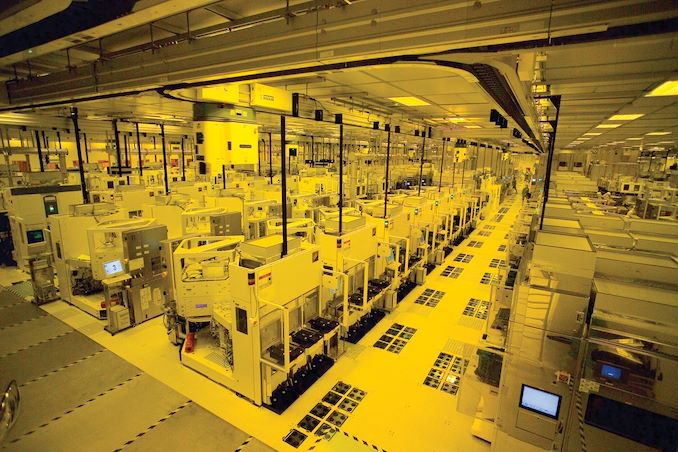
Set to be strategically positioned near TSMC's upcoming Fab 21 complex in Arizona, Amkor's Peoria facility will occupy 55 acres and, when fully completed, will feature over 500,000 square feet (46,451 square meters) of cleanroom space, more than twice the size of Amkor's advanced packaging site in Vietnam. Although the company has not disclosed the exact capacity or the specific technologies the facility will support, it is expected to cater to a wide range of industries, including automotive, high-performance computing, and mobile technologies. This suggests the new plant will offer diverse packaging solutions, including traditional, 2.5D, and 3D technologies.
Amkor has collaborated extensively with Apple on the vision and initial setup of the Peoria facility, as Apple is slated to be the facility's first and largest customer, marking a significant commitment from the tech giant. This partnership highlights the importance of the new facility in reinforcing the U.S. semiconductor supply chain and positioning Amkor as a key partner for companies relying on TSMC's manufacturing capabilities. The project is expected to generate around 2,000 jobs and is scheduled to begin operations in 2027.
This week SK hynix also signed a preliminary agreement with the U.S. government to receive up to $450 million in direct funding and $500 million in loans to build an advanced memory packaging facility in West Lafayette, Indiana.
The proposed facility is scheduled to begin operations in 2028, which means that it will assemble HBM4 or HBM4E memory. Meanwhile, DRAM devices for high bandwidth memory (HBM) stacks will still be produced in South Korea. Nonetheless, packing finished HBM4/HBM4E in the U.S. and possibly integrating these memory modules with high-end processors is a big deal.
In addition to building its packaging plant, SK hynix plans to collaborate with Purdue University and other local research institutions to advance semiconductor technology and packaging innovations. This partnership is intended to bolster research and development in the region, positioning the facility as a hub for AI technology and skilled employment.
Semiconductors

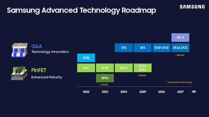
Samsung this week has unveiled its latest process technologies roadmap at the company's Samsung Foundry Forum (SFF) U.S. The new plan covers the evolution of Samsung's 2nm-class production nodes through 2027, including a process technology with a backside power delivery, re-emphasizing plans to bring out a 1.4nm-class node in 2027, and the introduction of a 'high value' 4nm-class manufacturing tech.
Samsung Foundry's key announcements for today are clearly focused on the its 2nm-class process technologies, which are set to enter production in 2025 and will span to 2027, when the company's 1.4-nm class production node is set to enter the scene. Samsung is also adding (or rather, renaming) another 2nm-class node to their roadmap with SF2, which was previously disclosed by Samsung as SF3P and aimed at high-performance devices.
"We have refined and improved the SF3P, resulting in what we now refer to as SF2," a Samsung spokesperson told AnandTech. "This enhanced node incorporates various process design improvements, delivering notable power, performance, and area (PPA) benefits."
| Samsung Foundry for Leading-Edge Nodes Announced on June 12, 2024 Compiled by AnandTech |
||||||||
| HVM Start | 2023 | 2024 | 2025 | 2026 | 2027 | 2027 | ||
| Process | SF3E | SF3 | SF2 (aka SF3P) |
SF2P/SF2X | SF2Z | SF1.4 | ||
| FET | GAAFET | |||||||
| Power Delivery | Frontside | Backside (BSPDN) | ? | |||||
| EUV | 0.33 NA EUV | ? | ? | ? | ? | |||
This is another example of a rebranding of leading-edge fabrication nodes in the recent years by a major chipmaker. Samsung Foundry is not disclosing any specific PPA improvements SF3P has over SF2, and for now is only stating in high-level terms that it will be a better-performing node than the planned SF3P.
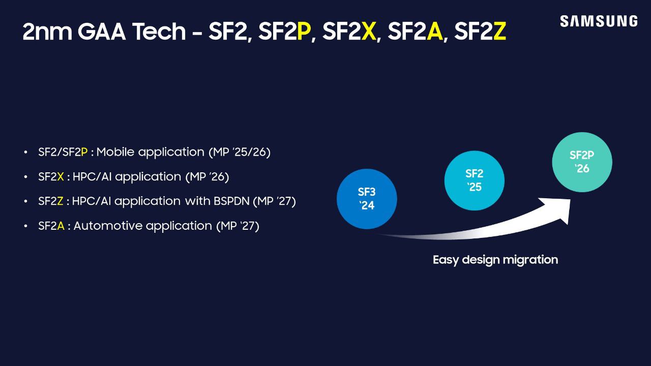
Meanwhile, this week's announcement also includes new information on Samsung's next batch of process nodes, which are planned for 2026 and 2027. In 2026 Samsung will have SF2P, a further refinement of SF2 which incorporates 'faster' yet less dense transistors. That will be followed up in 2027 with SF2Z, which adds backside power delivery to the mix for better and higher quality power delivery. In particular, Samsung is targetting voltate drop (aka IR drop) here, which is an ongoing concern in chip design.
Finally, SF1.4, a 1.4nm-class node, is on track for 2027 as well. Interestingly, however, it looks like it does not feature a backside power delivery. Which, per current roadmaps, would have Samsung as the only foundry not using BSPDN for their first 1.4nm/14Å-class node.
"We have optimized BSPDN and incorporated it for the first time in the SF2Z node we announced today," the spokesperso... Semiconductors

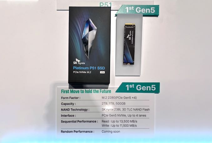
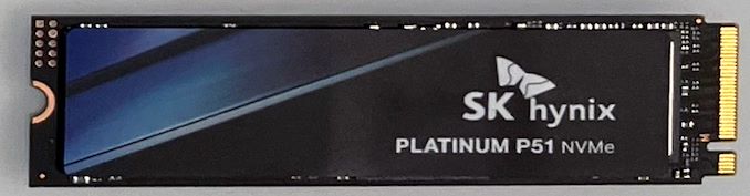
SK hynix is set to unveil their first Gen5 consumer NVMe SSD lineup shortly, based on the products at display in their GTC 2024 booth. The Platinum P51 M.2 2280 NVMe SSD will take over flagship duties from the Platinum P41 that has been serving the market for more than a year.
Similar to the Gold P31 and the Platinum P41, the Platinum P51 also uses an in-house SSD controller. The key updates are the move to PCIe Gen5 and the use of SK hynix's 238L TLC NAND. Other details are scarce, and we have reached out for additional information.
| SK hynix Platinum P51 Gen5 NVMe SSD Specifications | ||||
| Capacity | 500 GB | 1 TB | 2 TB | |
| Controller | SK hynix In-House (Alistar) | |||
| NAND Flash | SK hynix 238L 3D TLC NAND at ?? MT/s ('4D' with CMOS circuitry under the NAND as per SK hynix marketing) | |||
| Form-Factor, Interface | M.2-2280, PCIe 5.0 x4, NVMe 2.0 | |||
| Sequential Read | 13500 MB/s | |||
| Sequential Write | 11500 MB/s | |||
| Random Read IOPS | TBD | |||
| Random Write IOPS | TBD | |||
| SLC Caching | Yes | |||
| TCG Opal Encryption | TBD | |||
| Warranty | TBD | |||
| Write Endurance | TBD | TBD | TBD | |
Only the peak sequential access numbers were available at the GTC booth, indicating that the drive's firmware is still undergoing tweaks. It is also unclear how these numbers are going to vary based on capacity. Availability and pricing are also not public yet.
This is a significant launch for the Gen5 consumer SSD market, where the number of available options are quite limited. The Phison E26 controller and Micron's B58R NAND combination is already in its second generation (with the NAND operating at 2400 MT/s in the newest avatar), but other vertically integrated vendors such as Samsung, Western Digital / Kioxia, and SK hynix (till now) are focusing more on the Gen4 market which has much higher adoption.
We will update the piece with additional information once the specifications are officially available.
Storage
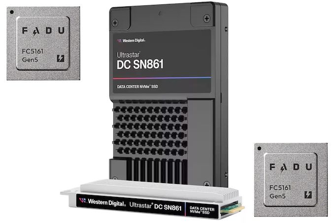
When Western Digital introduced its Ultrastar DC SN861 SSDs earlier this year, the company did not disclose which controller it used for these drives, which made many observers presume that WD was using an in-house controller. But a recent teardown of the drive shows that is not the case; instead, the company is using a controller from Fadu, a South Korean company founded in 2015 that specializes on enterprise-grade turnkey SSD solutions.
The Western Digital Ultrastar DC SN861 SSD is aimed at performance-hungry hyperscale datacenters and enterprise customers which are adopting PCIe Gen5 storage devices these days. And, as uncovered in photos from a recent Storage Review article, the drive is based on Fadu's FC5161 NVMe 2.0-compliant controller. The FC5161 utilizes 16 NAND channels supporting an ONFi 5.0 2400 MT/s interface, and features a combination of enterprise-grade capabilities (OCP Cloud Spec 2.0, SR-IOV, up to 512 name spaces for ZNS support, flexible data placement, NVMe-MI 1.2, advanced security, telemetry, power loss protection) not available on other off-the-shelf controllers – or on any previous Western Digital controllers.
The Ultrastar DC SN861 SSD offers sequential read speeds up to 13.7 GB/s as well as sequential write speeds up to 7.5 GB/s. As for random performance, it boasts with an up to 3.3 million random 4K read IOPS and up to 0.8 million random 4K write IOPS. The drives are available in capacities between 1.6 TB and 7.68 TB with one or three drive writes per day (DWPD) over five years rating as well as in U.2 and E1.S form-factors.
While the two form factors of the SN861 share a similar technical design, Western Digital has tailored each version for distinct workloads: the E1.S supports FDP and performance enhancements specifically for cloud environments. By contrast, the U.2 model is geared towards high-performance enterprise tasks and emerging applications like AI.
Without any doubts, Western Digital's Ultrastar DC SN861 is a feature-rich high-performance enterprise-grade SSD. It has another distinctive feature: a 5W idle power consumption, which is rather low by the standards of enterprise-grade drives (e.g., it is 1W lower compared to the SN840). While the difference with predecessors may be just 1W, hyperscalers deploy thousands of drives and for their TCO every watt counts.
Western Digital's Ultrastar DC SN861 SSDs are now available for purchase to select customers (such as Meta) and to interested parties. Prices are unknown, but they will depend on such factors as volumes.
Sources: Fadu, Storage Review
Storage
Samsung this week has unveiled its latest process technologies roadmap at the company's Samsung Foundry Forum (SFF) U.S. The new plan covers the evolution of Samsung's 2nm-class production nodes through 2027, including a process technology with a backside power delivery, re-emphasizing plans to bring out a 1.4nm-class node in 2027, and the introduction of a 'high value' 4nm-class manufacturing tech.
Samsung Foundry's key announcements for today are clearly focused on the its 2nm-class process technologies, which are set to enter production in 2025 and will span to 2027, when the company's 1.4-nm class production node is set to enter the scene. Samsung is also adding (or rather, renaming) another 2nm-class node to their roadmap with SF2, which was previously disclosed by Samsung as SF3P and aimed at high-performance devices.
"We have refined and improved the SF3P, resulting in what we now refer to as SF2," a Samsung spokesperson told AnandTech. "This enhanced node incorporates various process design improvements, delivering notable power, performance, and area (PPA) benefits."
| Samsung Foundry for Leading-Edge Nodes Announced on June 12, 2024 Compiled by AnandTech |
||||||||
| HVM Start | 2023 | 2024 | 2025 | 2026 | 2027 | 2027 | ||
| Process | SF3E | SF3 | SF2 (aka SF3P) |
SF2P/SF2X | SF2Z | SF1.4 | ||
| FET | GAAFET | |||||||
| Power Delivery | Frontside | Backside (BSPDN) | ? | |||||
| EUV | 0.33 NA EUV | ? | ? | ? | ? | |||
This is another example of a rebranding of leading-edge fabrication nodes in the recent years by a major chipmaker. Samsung Foundry is not disclosing any specific PPA improvements SF3P has over SF2, and for now is only stating in high-level terms that it will be a better-performing node than the planned SF3P.
Meanwhile, this week's announcement also includes new information on Samsung's next batch of process nodes, which are planned for 2026 and 2027. In 2026 Samsung will have SF2P, a further refinement of SF2 which incorporates 'faster' yet less dense transistors. That will be followed up in 2027 with SF2Z, which adds backside power delivery to the mix for better and higher quality power delivery. In particular, Samsung is targetting voltate drop (aka IR drop) here, which is an ongoing concern in chip design.
Finally, SF1.4, a 1.4nm-class node, is on track for 2027 as well. Interestingly, however, it looks like it does not feature a backside power delivery. Which, per current roadmaps, would have Samsung as the only foundry not using BSPDN for their first 1.4nm/14Å-class node.
"We have optimized BSPDN and incorporated it for the first time in the SF2Z node we announced today," the spokesperso... Semiconductors
SK hynix is set to unveil their first Gen5 consumer NVMe SSD lineup shortly, based on the products at display in their GTC 2024 booth. The Platinum P51 M.2 2280 NVMe SSD will take over flagship duties from the Platinum P41 that has been serving the market for more than a year.
Similar to the Gold P31 and the Platinum P41, the Platinum P51 also uses an in-house SSD controller. The key updates are the move to PCIe Gen5 and the use of SK hynix's 238L TLC NAND. Other details are scarce, and we have reached out for additional information.
| SK hynix Platinum P51 Gen5 NVMe SSD Specifications | ||||
| Capacity | 500 GB | 1 TB | 2 TB | |
| Controller | SK hynix In-House (Alistar) | |||
| NAND Flash | SK hynix 238L 3D TLC NAND at ?? MT/s ('4D' with CMOS circuitry under the NAND as per SK hynix marketing) | |||
| Form-Factor, Interface | M.2-2280, PCIe 5.0 x4, NVMe 2.0 | |||
| Sequential Read | 13500 MB/s | |||
| Sequential Write | 11500 MB/s | |||
| Random Read IOPS | TBD | |||
| Random Write IOPS | TBD | |||
| SLC Caching | Yes | |||
| TCG Opal Encryption | TBD | |||
| Warranty | TBD | |||
| Write Endurance | TBD | TBD | TBD | |
Only the peak sequential access numbers were available at the GTC booth, indicating that the drive's firmware is still undergoing tweaks. It is also unclear how these numbers are going to vary based on capacity. Availability and pricing are also not public yet.
This is a significant launch for the Gen5 consumer SSD market, where the number of available options are quite limited. The Phison E26 controller and Micron's B58R NAND combination is already in its second generation (with the NAND operating at 2400 MT/s in the newest avatar), but other vertically integrated vendors such as Samsung, Western Digital / Kioxia, and SK hynix (till now) are focusing more on the Gen4 market which has much higher adoption.
We will update the piece with additional information once the specifications are officially available.
Storage
When Western Digital introduced its Ultrastar DC SN861 SSDs earlier this year, the company did not disclose which controller it used for these drives, which made many observers presume that WD was using an in-house controller. But a recent teardown of the drive shows that is not the case; instead, the company is using a controller from Fadu, a South Korean company founded in 2015 that specializes on enterprise-grade turnkey SSD solutions.
The Western Digital Ultrastar DC SN861 SSD is aimed at performance-hungry hyperscale datacenters and enterprise customers which are adopting PCIe Gen5 storage devices these days. And, as uncovered in photos from a recent Storage Review article, the drive is based on Fadu's FC5161 NVMe 2.0-compliant controller. The FC5161 utilizes 16 NAND channels supporting an ONFi 5.0 2400 MT/s interface, and features a combination of enterprise-grade capabilities (OCP Cloud Spec 2.0, SR-IOV, up to 512 name spaces for ZNS support, flexible data placement, NVMe-MI 1.2, advanced security, telemetry, power loss protection) not available on other off-the-shelf controllers – or on any previous Western Digital controllers.
The Ultrastar DC SN861 SSD offers sequential read speeds up to 13.7 GB/s as well as sequential write speeds up to 7.5 GB/s. As for random performance, it boasts with an up to 3.3 million random 4K read IOPS and up to 0.8 million random 4K write IOPS. The drives are available in capacities between 1.6 TB and 7.68 TB with one or three drive writes per day (DWPD) over five years rating as well as in U.2 and E1.S form-factors.
While the two form factors of the SN861 share a similar technical design, Western Digital has tailored each version for distinct workloads: the E1.S supports FDP and performance enhancements specifically for cloud environments. By contrast, the U.2 model is geared towards high-performance enterprise tasks and emerging applications like AI.
Without any doubts, Western Digital's Ultrastar DC SN861 is a feature-rich high-performance enterprise-grade SSD. It has another distinctive feature: a 5W idle power consumption, which is rather low by the standards of enterprise-grade drives (e.g., it is 1W lower compared to the SN840). While the difference with predecessors may be just 1W, hyperscalers deploy thousands of drives and for their TCO every watt counts.
Western Digital's Ultrastar DC SN861 SSDs are now available for purchase to select customers (such as Meta) and to interested parties. Prices are unknown, but they will depend on such factors as volumes.
Sources: Fadu, Storage Review
Storage
Lorem Ipsum is simply dummy text of the printing and typesetting industry. Lorem Ipsum has been the industry's.
Samsung this week has unveiled its latest process technologies roadmap at the company's Samsung Foundry Forum (SFF) U.S. The new plan covers the evolution of Samsung's 2nm-class production nodes through 2027, including a process technology with a backside power delivery, re-emphasizing plans to bring out a 1.4nm-class node in 2027, and the introduction of a 'high value' 4nm-class manufacturing tech.
Samsung Foundry's key announcements for today are clearly focused on the its 2nm-class process technologies, which are set to enter production in 2025 and will span to 2027, when the company's 1.4-nm class production node is set to enter the scene. Samsung is also adding (or rather, renaming) another 2nm-class node to their roadmap with SF2, which was previously disclosed by Samsung as SF3P and aimed at high-performance devices.
"We have refined and improved the SF3P, resulting in what we now refer to as SF2," a Samsung spokesperson told AnandTech. "This enhanced node incorporates various process design improvements, delivering notable power, performance, and area (PPA) benefits."
| Samsung Foundry for Leading-Edge Nodes Announced on June 12, 2024 Compiled by AnandTech |
||||||||
| HVM Start | 2023 | 2024 | 2025 | 2026 | 2027 | 2027 | ||
| Process | SF3E | SF3 | SF2 (aka SF3P) |
SF2P/SF2X | SF2Z | SF1.4 | ||
| FET | GAAFET | |||||||
| Power Delivery | Frontside | Backside (BSPDN) | ? | |||||
| EUV | 0.33 NA EUV | ? | ? | ? | ? | |||
This is another example of a rebranding of leading-edge fabrication nodes in the recent years by a major chipmaker. Samsung Foundry is not disclosing any specific PPA improvements SF3P has over SF2, and for now is only stating in high-level terms that it will be a better-performing node than the planned SF3P.
Meanwhile, this week's announcement also includes new information on Samsung's next batch of process nodes, which are planned for 2026 and 2027. In 2026 Samsung will have SF2P, a further refinement of SF2 which incorporates 'faster' yet less dense transistors. That will be followed up in 2027 with SF2Z, which adds backside power delivery to the mix for better and higher quality power delivery. In particular, Samsung is targetting voltate drop (aka IR drop) here, which is an ongoing concern in chip design.
Finally, SF1.4, a 1.4nm-class node, is on track for 2027 as well. Interestingly, however, it looks like it does not feature a backside power delivery. Which, per current roadmaps, would have Samsung as the only foundry not using BSPDN for their first 1.4nm/14Å-class node.
"We have optimized BSPDN and incorporated it for the first time in the SF2Z node we announced today," the spokesperso... Semiconductors
SK hynix is set to unveil their first Gen5 consumer NVMe SSD lineup shortly, based on the products at display in their GTC 2024 booth. The Platinum P51 M.2 2280 NVMe SSD will take over flagship duties from the Platinum P41 that has been serving the market for more than a year.
Similar to the Gold P31 and the Platinum P41, the Platinum P51 also uses an in-house SSD controller. The key updates are the move to PCIe Gen5 and the use of SK hynix's 238L TLC NAND. Other details are scarce, and we have reached out for additional information.
| SK hynix Platinum P51 Gen5 NVMe SSD Specifications | ||||
| Capacity | 500 GB | 1 TB | 2 TB | |
| Controller | SK hynix In-House (Alistar) | |||
| NAND Flash | SK hynix 238L 3D TLC NAND at ?? MT/s ('4D' with CMOS circuitry under the NAND as per SK hynix marketing) | |||
| Form-Factor, Interface | M.2-2280, PCIe 5.0 x4, NVMe 2.0 | |||
| Sequential Read | 13500 MB/s | |||
| Sequential Write | 11500 MB/s | |||
| Random Read IOPS | TBD | |||
| Random Write IOPS | TBD | |||
| SLC Caching | Yes | |||
| TCG Opal Encryption | TBD | |||
| Warranty | TBD | |||
| Write Endurance | TBD | TBD | TBD | |
Only the peak sequential access numbers were available at the GTC booth, indicating that the drive's firmware is still undergoing tweaks. It is also unclear how these numbers are going to vary based on capacity. Availability and pricing are also not public yet.
This is a significant launch for the Gen5 consumer SSD market, where the number of available options are quite limited. The Phison E26 controller and Micron's B58R NAND combination is already in its second generation (with the NAND operating at 2400 MT/s in the newest avatar), but other vertically integrated vendors such as Samsung, Western Digital / Kioxia, and SK hynix (till now) are focusing more on the Gen4 market which has much higher adoption.
We will update the piece with additional information once the specifications are officially available.
Storage
When Western Digital introduced its Ultrastar DC SN861 SSDs earlier this year, the company did not disclose which controller it used for these drives, which made many observers presume that WD was using an in-house controller. But a recent teardown of the drive shows that is not the case; instead, the company is using a controller from Fadu, a South Korean company founded in 2015 that specializes on enterprise-grade turnkey SSD solutions.
The Western Digital Ultrastar DC SN861 SSD is aimed at performance-hungry hyperscale datacenters and enterprise customers which are adopting PCIe Gen5 storage devices these days. And, as uncovered in photos from a recent Storage Review article, the drive is based on Fadu's FC5161 NVMe 2.0-compliant controller. The FC5161 utilizes 16 NAND channels supporting an ONFi 5.0 2400 MT/s interface, and features a combination of enterprise-grade capabilities (OCP Cloud Spec 2.0, SR-IOV, up to 512 name spaces for ZNS support, flexible data placement, NVMe-MI 1.2, advanced security, telemetry, power loss protection) not available on other off-the-shelf controllers – or on any previous Western Digital controllers.
The Ultrastar DC SN861 SSD offers sequential read speeds up to 13.7 GB/s as well as sequential write speeds up to 7.5 GB/s. As for random performance, it boasts with an up to 3.3 million random 4K read IOPS and up to 0.8 million random 4K write IOPS. The drives are available in capacities between 1.6 TB and 7.68 TB with one or three drive writes per day (DWPD) over five years rating as well as in U.2 and E1.S form-factors.
While the two form factors of the SN861 share a similar technical design, Western Digital has tailored each version for distinct workloads: the E1.S supports FDP and performance enhancements specifically for cloud environments. By contrast, the U.2 model is geared towards high-performance enterprise tasks and emerging applications like AI.
Without any doubts, Western Digital's Ultrastar DC SN861 is a feature-rich high-performance enterprise-grade SSD. It has another distinctive feature: a 5W idle power consumption, which is rather low by the standards of enterprise-grade drives (e.g., it is 1W lower compared to the SN840). While the difference with predecessors may be just 1W, hyperscalers deploy thousands of drives and for their TCO every watt counts.
Western Digital's Ultrastar DC SN861 SSDs are now available for purchase to select customers (such as Meta) and to interested parties. Prices are unknown, but they will depend on such factors as volumes.
Sources: Fadu, Storage Review
Storage

![TSMC to Expand Specialty Capacity by 50%, Introduce 4nm N4e Low-Power Node <p align="center"><a href="https://www.anandtech.com/show/21397/tsmc-to-expand-specialty-capacity-by-50-introduce-4nm-lowpower-node"><img src="https://images.anandtech.com/doci/21397/tsmc-semiconductor-fab-wafer-1-678_575px.jpg" alt="" /></a></p><p><p>With all the new fabs being built in Germany and Japan, as well as the expansion of production capacity in China, TSMC is planning to extend its production capacity for specialty technologies by 50% by 2027. As disclosed by the company during its European Technology Symposium this week, TSMC expects to need to not only convert existing capacity to meet demands for specialty processes, but even build new (greenfield) fab space just for this purpose. One of the big drivers for this demand, in turn, will be TSMC's next specialty node: N4e, a 4nm-class ultra-low-power production node.</p>
<p>"In the past, we always did the review phase [for upcoming fabs], but for the first time in a long time at TSMC, we started building greenfield fab that will address the future specialty technology requirements," said Dr. Kevin Zhang, Senior Vice President, Business Development and Overseas Operations Office, at the event. "In the next four to five years, we actually going to grow our specialty capacity by up to 1.5x. In doing so we actually expanding the footprint of our manufacturing network to improve the resiliency of the overall fab supply chain."</p>
<p>On top of its well-known major logic nodes like N5 and N3E, TSMC also offers a suite of specialty nodes for applications such as power semiconductors, mixed analog I/O, and ultra-low-power applications (e.g. IoT). These are typically based on the company's trailing manufacturing processes, but regardless of the underlying technology, the capacity demand for these nodes is growing right alongside the demand for TSMC's major logic nodes. All of which has required TSMC to reevaluate how they go about planning for capacity on their specialty nodes.</p>
<p>TSMC's expansion strategy in the recent years has pursued several goals. One of them has been to build new fabs outside of Taiwan; another has been to generally expand production capacity to meet future demand for all types of process technologies – which is why the company is building up capacity for specialty nodes.</p>
<p>At present, TSMC's most advanced specialty node is N6e, an N7/N6 variant that supports operating voltages between 0.4V and 0.9V. With N4e, TSMC is looking at voltages below 0.4V. Though for now, TSMC is not disclosing much in the way of technical details for the planned node; given the company's history here, we expect they'll have more to talk about next year once the new process is ready.</p>
</p> Semiconductors](https://lh3.googleusercontent.com/blogger_img_proxy/AEn0k_vqKUknDdbkLOodKI8EG5tDXU1paxLgu6C3qaTJOPDR3MzW6JABC1CDxlntPDSAmAYP0G6C5jExNpwB6iVFL9KFoXgFI045nxQm8GkbO_p7DJm7u5-PGZUPjgg3TxdgptlU4HG7Bf_tGSqGMmAPAHUGHj-aNHccAg=w72-h72-p-k-no-nu)
 of cleanroom space, more than twice the size of Amkor's advanced packaging site in Vietnam. Although the company has not disclosed the exact capacity or the specific technologies the facility will support, it is expected to cater to a wide range of industries, including automotive, high-performance computing, and mobile technologies. This suggests the new plant will offer diverse packaging solutions, including traditional, 2.5D, and 3D technologies.</p>
<p>Amkor has collaborated extensively with Apple on the vision and initial setup of the Peoria facility, as Apple is slated to be the facility's first and largest customer, marking a significant commitment from the tech giant. This partnership highlights the importance of the new facility in reinforcing the U.S. semiconductor supply chain and positioning Amkor as a key partner for companies relying on TSMC's manufacturing capabilities. The project is expected to generate around 2,000 jobs and is scheduled to begin operations in 2027. </p>
<h3>SK hynix to Build HBM4 in the U.S.</h3>
<p>This week SK hynix also signed a preliminary agreement with the U.S. government to receive up to $450 million in direct funding and $500 million in loans to build an advanced memory packaging facility in West Lafayette, Indiana. </p>
<p>The proposed facility is scheduled to begin operations in 2028, which means that it will assemble HBM4 or HBM4E memory. Meanwhile, DRAM devices for high bandwidth memory (HBM) stacks will still be produced in South Korea. Nonetheless, packing finished HBM4/HBM4E in the U.S. and possibly integrating these memory modules with high-end processors is a big deal.</p>
<p>In addition to building its packaging plant, SK hynix plans to collaborate with Purdue University and other local research institutions to advance semiconductor technology and packaging innovations. This partnership is intended to bolster research and development in the region, positioning the facility as a hub for AI technology and skilled employment.</p>
<p>Sources: <a href="https://ir.amkor.com/news-releases/news-release-details/amkor-signs-preliminary-memorandum-terms-us-department-commerce">Amkor</a>, <a href="https://news.skhynix.com/preliminary-mou-terms-signed-with-us-doc-for-advanced-packaging-facility-in-indiana/">SK hynix</a></p>
</p> Semiconductors)
 of cleanroom space, more than twice the size of Amkor's advanced packaging site in Vietnam. Although the company has not disclosed the exact capacity or the specific technologies the facility will support, it is expected to cater to a wide range of industries, including automotive, high-performance computing, and mobile technologies. This suggests the new plant will offer diverse packaging solutions, including traditional, 2.5D, and 3D technologies.</p>
<p>Amkor has collaborated extensively with Apple on the vision and initial setup of the Peoria facility, as Apple is slated to be the facility's first and largest customer, marking a significant commitment from the tech giant. This partnership highlights the importance of the new facility in reinforcing the U.S. semiconductor supply chain and positioning Amkor as a key partner for companies relying on TSMC's manufacturing capabilities. The project is expected to generate around 2,000 jobs and is scheduled to begin operations in 2027. </p>
<h3>SK hynix to Build HBM4 in the U.S.</h3>
<p>This week SK hynix also signed a preliminary agreement with the U.S. government to receive up to $450 million in direct funding and $500 million in loans to build an advanced memory packaging facility in West Lafayette, Indiana. </p>
<p>The proposed facility is scheduled to begin operations in 2028, which means that it will assemble HBM4 or HBM4E memory. Meanwhile, DRAM devices for high bandwidth memory (HBM) stacks will still be produced in South Korea. Nonetheless, packing finished HBM4/HBM4E in the U.S. and possibly integrating these memory modules with high-end processors is a big deal.</p>
<p>In addition to building its packaging plant, SK hynix plans to collaborate with Purdue University and other local research institutions to advance semiconductor technology and packaging innovations. This partnership is intended to bolster research and development in the region, positioning the facility as a hub for AI technology and skilled employment.</p>
<p>Sources: <a href="https://ir.amkor.com/news-releases/news-release-details/amkor-signs-preliminary-memorandum-terms-us-department-commerce">Amkor</a>, <a href="https://news.skhynix.com/preliminary-mou-terms-signed-with-us-doc-for-advanced-packaging-facility-in-indiana/">SK hynix</a></p>
</p> Semiconductors)
 of cleanroom space, more than twice the size of Amkor's advanced packaging site in Vietnam. Although the company has not disclosed the exact capacity or the specific technologies the facility will support, it is expected to cater to a wide range of industries, including automotive, high-performance computing, and mobile technologies. This suggests the new plant will offer diverse packaging solutions, including traditional, 2.5D, and 3D technologies.</p>
<p>Amkor has collaborated extensively with Apple on the vision and initial setup of the Peoria facility, as Apple is slated to be the facility's first and largest customer, marking a significant commitment from the tech giant. This partnership highlights the importance of the new facility in reinforcing the U.S. semiconductor supply chain and positioning Amkor as a key partner for companies relying on TSMC's manufacturing capabilities. The project is expected to generate around 2,000 jobs and is scheduled to begin operations in 2027. </p>
<h3>SK hynix to Build HBM4 in the U.S.</h3>
<p>This week SK hynix also signed a preliminary agreement with the U.S. government to receive up to $450 million in direct funding and $500 million in loans to build an advanced memory packaging facility in West Lafayette, Indiana. </p>
<p>The proposed facility is scheduled to begin operations in 2028, which means that it will assemble HBM4 or HBM4E memory. Meanwhile, DRAM devices for high bandwidth memory (HBM) stacks will still be produced in South Korea. Nonetheless, packing finished HBM4/HBM4E in the U.S. and possibly integrating these memory modules with high-end processors is a big deal.</p>
<p>In addition to building its packaging plant, SK hynix plans to collaborate with Purdue University and other local research institutions to advance semiconductor technology and packaging innovations. This partnership is intended to bolster research and development in the region, positioning the facility as a hub for AI technology and skilled employment.</p>
<p>Sources: <a href="https://ir.amkor.com/news-releases/news-release-details/amkor-signs-preliminary-memorandum-terms-us-department-commerce">Amkor</a>, <a href="https://news.skhynix.com/preliminary-mou-terms-signed-with-us-doc-for-advanced-packaging-facility-in-indiana/">SK hynix</a></p>
</p> Semiconductors | https://compbuddey.blogspot.com/2024/11/us-signs-15b-in-chips-act-agreements_12.html)
 of cleanroom space, more than twice the size of Amkor's advanced packaging site in Vietnam. Although the company has not disclosed the exact capacity or the specific technologies the facility will support, it is expected to cater to a wide range of industries, including automotive, high-performance computing, and mobile technologies. This suggests the new plant will offer diverse packaging solutions, including traditional, 2.5D, and 3D technologies.</p>
<p>Amkor has collaborated extensively with Apple on the vision and initial setup of the Peoria facility, as Apple is slated to be the facility's first and largest customer, marking a significant commitment from the tech giant. This partnership highlights the importance of the new facility in reinforcing the U.S. semiconductor supply chain and positioning Amkor as a key partner for companies relying on TSMC's manufacturing capabilities. The project is expected to generate around 2,000 jobs and is scheduled to begin operations in 2027. </p>
<h3>SK hynix to Build HBM4 in the U.S.</h3>
<p>This week SK hynix also signed a preliminary agreement with the U.S. government to receive up to $450 million in direct funding and $500 million in loans to build an advanced memory packaging facility in West Lafayette, Indiana. </p>
<p>The proposed facility is scheduled to begin operations in 2028, which means that it will assemble HBM4 or HBM4E memory. Meanwhile, DRAM devices for high bandwidth memory (HBM) stacks will still be produced in South Korea. Nonetheless, packing finished HBM4/HBM4E in the U.S. and possibly integrating these memory modules with high-end processors is a big deal.</p>
<p>In addition to building its packaging plant, SK hynix plans to collaborate with Purdue University and other local research institutions to advance semiconductor technology and packaging innovations. This partnership is intended to bolster research and development in the region, positioning the facility as a hub for AI technology and skilled employment.</p>
<p>Sources: <a href="https://ir.amkor.com/news-releases/news-release-details/amkor-signs-preliminary-memorandum-terms-us-department-commerce">Amkor</a>, <a href="https://news.skhynix.com/preliminary-mou-terms-signed-with-us-doc-for-advanced-packaging-facility-in-indiana/">SK hynix</a></p>
</p> Semiconductors&body=https://compbuddey.blogspot.com/2024/11/us-signs-15b-in-chips-act-agreements_12.html)


0 Comments