
As the deployment of PCIe 5.0 picks up steam in both datacenter and consumer markets, PCI-SIG is not sitting idle, and is already working on getting the ecosystem ready for the updats to the PCIe specifications. At FMS 2024, some vendors were even talking about PCIe 7.0 with its 128 GT/s capabilities despite PCIe 6.0 not even starting to ship yet. We caught up with PCI-SIG to get some updates on its activities and have a discussion on the current state of the PCIe ecosystem.
PCI-SIG has already made the PCIe 7.0 specifications (v 0.5) available to its members, and expects full specifications to be officially released sometime in 2025. The goal is to deliver a 128 GT/s data rate with up to 512 GBps of bidirectional traffic using x16 links. Similar to PCIe 6.0, this specification will also utilize PAM4 signaling and maintain backwards compatibility. Power efficiency as well as silicon die area are also being kept in mind as part of the drafting process.
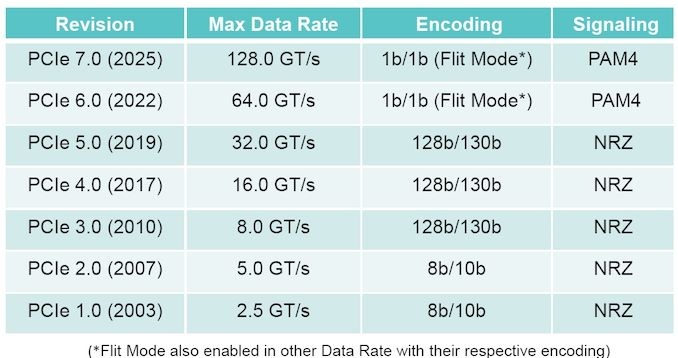
The move to PAM4 signaling brings higher bit-error rates compared to the previous NRZ scheme. This made it necessary to adopt a different error correction scheme in PCIe 6.0 - instead of operating on variable length packets, PCIe 6.0's Flow Control Unit (FLIT) encoding operates on fixed size packets to aid in forward error correction. PCIe 7.0 retains these aspects.
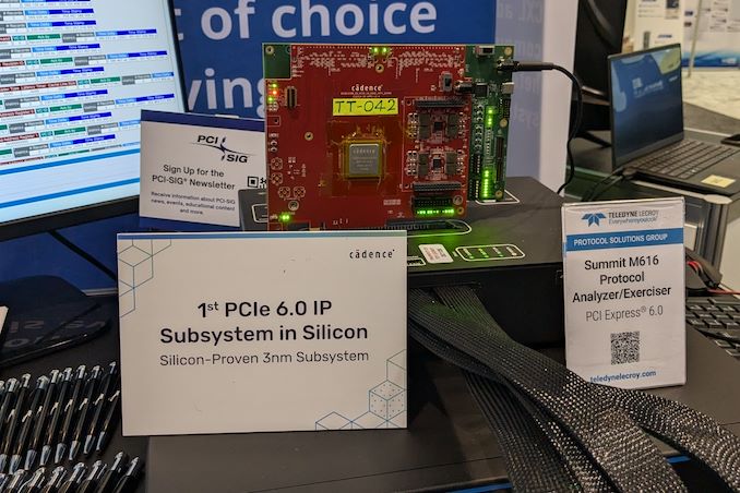
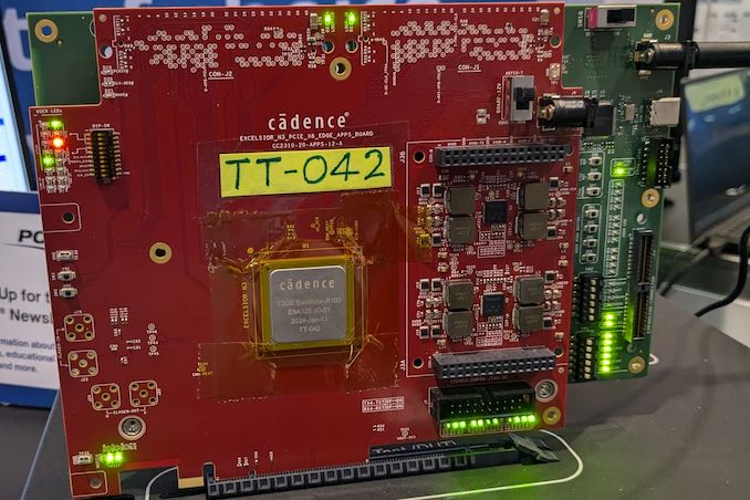
The integrators list for the PCIe 6.0 compliance program is also expected to come out in 2025, though initial testing is already in progress. This was evident by the FMS 2024 demo involving Cadence's 3nm test chip for its PCIe 6.0 IP offering along with Teledyne Lecroy's PCIe 6.0 analyzer. These timelines track well with the specification completion dates and compliance program availability for previous PCIe generations.
We also received an update on the optical workgroup - while being optical-technology agnostic, the WG also intends to develop technology-specific form-factors including pluggable optical transceivers, on-board optics, co-packaged optics, and optical I/O. The logical and electrical layers of the PCIe 6.0 specifications are being enhanced to accommodate the new optical PCIe standardization and this process will also be done with PCIe 7.0 to coincide with that standard's release next year.
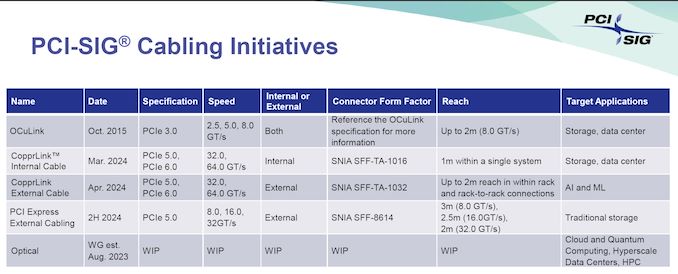
The PCI-SIG also has ongoing cabling initiatives. On the consumer side, we have seen significant traction for Thunderbolt and external GPU enclosures. However, even datacenters and enterprise systems are moving towards cabling solutions as it becomes evident that disaggregation of components such as storage from the CPU and GPU are better for thermal design. Additionally maintaining signal integrity over longer distances becomes difficult for on-board signal traces. Cabling internal to the computing systems can help here.
OCuLink emerged as a good candidate and was adopted fairly widely as an internal link in server systems. It has even made an appearance in mini-PCs from some Chinese manufacturers in its external avatar for the consumer market, albeit with limited traction. As speeds increase, a widely-adopted standard for external PCIe peripherals (or even connecting components within a system) will become imperative.
Storage
While the new CAMM and LPCAMM memory modules for laptops have garnered a great deal of attention in recent months, it's not just the mobile side of the PC memory industry that is looking at changes. The desktop memory market is also coming due for some upgrades to further improve DIMM performance, in the form of a new DIMM variety called the Clocked Unbuffered DIMM (CUDIMM). And while this memory isn't in use quite yet, several memory vendors had their initial CUDIMM products on display at this year's Computex trade show, offering a glimpse into the future of desktop memory.
A variation on traditional Unbuffered DIMMs (UDIMMs), Clocked UDIMMs (and Clocked SODIMMs) have been created as another solution to the ongoing signal integrity challenges presented by DDR5 memory. DDR5 allows for rather speedy transfer rates with removable (and easily installed) DIMMs, but further performance increases are running up against the laws of physics when it comes to the electrical challenges of supporting memory on a stick – particularly with so many capacity/performance combinations like we see today. And while those challenges aren't insurmountable, if DDR5 (and eventually, DDR6) are to keep increasing in speed, some changes appear to be needed to produce more electrically robust DIMMs, which is giving rise to the CUDIMM.
Standardized by JEDEC earlier this year as JESD323, CUDIMMs tweak the traditional unbuffered DIMM by adding a clock driver (CKD) to the DIMM itself, with the tiny IC responsible for regenerating the clock signal driving the actual memory chips. By generating a clean clock locally on the DIMM (rather than directly using the clock from the CPU, as is the case today), CUDIMMs are designed to offer improved stability and reliability at high memory speeds, combating the electrical issues that would otherwise cause reliability issues at faster memory speeds. In other words, adding a clock driver is the key to keeping DDR5 operating reliably at high clockspeeds.
All told, JEDEC is proposing that CUDIMMs be used for DDR5-6400 speeds and higher, with the first version of the specification covering speeds up to DDR5-7200. The new DIMMs will also be drop-in compatible with existing platforms (at least on paper), using the same 288-pin connector as today's standard DDR5 UDIMM and allowing for a relatively smooth transition towards higher DDR5 clockspeeds.
Memory

Samsung had quietly launched its BM1743 enterprise QLC SSD last month with a hefty 61.44 TB SKU. At FMS 2024, the company had the even larger 122.88 TB version of that SSD on display, alongside a few recorded benchmarking sessions. Compared to the previous generation, the BM1743 comes with a 4.1x improvement in I/O performance, improvement in data retention, and a 45% improvement in power efficiency for sequential writes.

The 128 TB-class QLC SSD boasts of sequential read speeds of 7.5 GBps and write speeds of 3 GBps. Random reads come in at 1.6 M IOPS, while 16 KB random writes clock in at 45K IOPS. Based on the quoted random write access granularity, it appears that Samsung is using a 16 KB indirection unit (IU) to optimize flash management. This is similar to the strategy adopted by Solidigm with IUs larger than 4K in their high-capacity SSDs.
A recorded benchmark session on the company's PM9D3a 8-channel Gen 5 SSD was also on display.

The SSD family is being promoted as a mainstream option for datacenters, and boasts of sequential reads up to 12 GBps and writes up to 6.8 GBps. Random reads clock in at 2 M IOPS, and random writes at 400 K IOPS.

Available in multiple form-factors up to 32 TB (M.2 tops out at 2 TB), the drive's firmware includes optional support for flexible data placement (FDP) to help address the write amplification aspect.
The PM1753 is the current enterprise SSD flagship in Samsung's lineup. With support for 16 NAND channels and capacities up to 32 TB, this U.2 / E3.S SSD has advertised sequential read and write speeds of 14.8 GBps and 11 GBps respectively. Random reads and writes for 4 KB accesses are listed at 3.4 M and 600 K IOPS.

Samsung claims a 1.7x performance improvement and a 1.7x power efficiency improvement over the previous generation (PM1743), making this TLC SSD suitable for AI servers.
The 9th Gen. V-NAND wafer was also available for viewing, though photography was prohibited. Mass production of this flash memory began in April 2024.
Storage
While the new CAMM and LPCAMM memory modules for laptops have garnered a great deal of attention in recent months, it's not just the mobile side of the PC memory industry that is looking at changes. The desktop memory market is also coming due for some upgrades to further improve DIMM performance, in the form of a new DIMM variety called the Clocked Unbuffered DIMM (CUDIMM). And while this memory isn't in use quite yet, several memory vendors had their initial CUDIMM products on display at this year's Computex trade show, offering a glimpse into the future of desktop memory.
A variation on traditional Unbuffered DIMMs (UDIMMs), Clocked UDIMMs (and Clocked SODIMMs) have been created as another solution to the ongoing signal integrity challenges presented by DDR5 memory. DDR5 allows for rather speedy transfer rates with removable (and easily installed) DIMMs, but further performance increases are running up against the laws of physics when it comes to the electrical challenges of supporting memory on a stick – particularly with so many capacity/performance combinations like we see today. And while those challenges aren't insurmountable, if DDR5 (and eventually, DDR6) are to keep increasing in speed, some changes appear to be needed to produce more electrically robust DIMMs, which is giving rise to the CUDIMM.
Standardized by JEDEC earlier this year as JESD323, CUDIMMs tweak the traditional unbuffered DIMM by adding a clock driver (CKD) to the DIMM itself, with the tiny IC responsible for regenerating the clock signal driving the actual memory chips. By generating a clean clock locally on the DIMM (rather than directly using the clock from the CPU, as is the case today), CUDIMMs are designed to offer improved stability and reliability at high memory speeds, combating the electrical issues that would otherwise cause reliability issues at faster memory speeds. In other words, adding a clock driver is the key to keeping DDR5 operating reliably at high clockspeeds.
All told, JEDEC is proposing that CUDIMMs be used for DDR5-6400 speeds and higher, with the first version of the specification covering speeds up to DDR5-7200. The new DIMMs will also be drop-in compatible with existing platforms (at least on paper), using the same 288-pin connector as today's standard DDR5 UDIMM and allowing for a relatively smooth transition towards higher DDR5 clockspeeds.
Memory
Samsung had quietly launched its BM1743 enterprise QLC SSD last month with a hefty 61.44 TB SKU. At FMS 2024, the company had the even larger 122.88 TB version of that SSD on display, alongside a few recorded benchmarking sessions. Compared to the previous generation, the BM1743 comes with a 4.1x improvement in I/O performance, improvement in data retention, and a 45% improvement in power efficiency for sequential writes.
The 128 TB-class QLC SSD boasts of sequential read speeds of 7.5 GBps and write speeds of 3 GBps. Random reads come in at 1.6 M IOPS, while 16 KB random writes clock in at 45K IOPS. Based on the quoted random write access granularity, it appears that Samsung is using a 16 KB indirection unit (IU) to optimize flash management. This is similar to the strategy adopted by Solidigm with IUs larger than 4K in their high-capacity SSDs.
A recorded benchmark session on the company's PM9D3a 8-channel Gen 5 SSD was also on display.
The SSD family is being promoted as a mainstream option for datacenters, and boasts of sequential reads up to 12 GBps and writes up to 6.8 GBps. Random reads clock in at 2 M IOPS, and random writes at 400 K IOPS.
Available in multiple form-factors up to 32 TB (M.2 tops out at 2 TB), the drive's firmware includes optional support for flexible data placement (FDP) to help address the write amplification aspect.
The PM1753 is the current enterprise SSD flagship in Samsung's lineup. With support for 16 NAND channels and capacities up to 32 TB, this U.2 / E3.S SSD has advertised sequential read and write speeds of 14.8 GBps and 11 GBps respectively. Random reads and writes for 4 KB accesses are listed at 3.4 M and 600 K IOPS.
Samsung claims a 1.7x performance improvement and a 1.7x power efficiency improvement over the previous generation (PM1743), making this TLC SSD suitable for AI servers.
The 9th Gen. V-NAND wafer was also available for viewing, though photography was prohibited. Mass production of this flash memory began in April 2024.
Storage

Kioxia's booth at FMS 2024 was a busy one with multiple technology demonstrations keeping visitors occupied. A walk-through of the BiCS 8 manufacturing process was the first to grab my attention. Kioxia and Western Digital announced the sampling of BiCS 8 in March 2023. We had touched briefly upon its CMOS Bonded Array (CBA) scheme in our coverage of Kioxial's 2Tb QLC NAND device and coverage of Western Digital's 128 TB QLC enterprise SSD proof-of-concept demonstration. At Kioxia's booth, we got more insights.

Traditionally, fabrication of flash chips involved placement of the associate logic circuitry (CMOS process) around the periphery of the flash array. The process then moved on to putting the CMOS under the cell array, but the wafer development process was serialized with the CMOS logic getting fabricated first followed by the cell array on top. However, this has some challenges because the cell array requires a high-temperature processing step to ensure higher reliability that can be detrimental to the health of the CMOS logic. Thanks to recent advancements in wafer bonding techniques, the new CBA process allows the CMOS wafer and cell array wafer to be processed independently in parallel and then pieced together, as shown in the models above.

The BiCS 8 3D NAND incorporates 218 layers, compared to 112 layers in BiCS 5 and 162 layers in BiCS 6. The company decided to skip over BiCS 7 (or, rather, it was probably a short-lived generation meant as an internal test vehicle). The generation retains the four-plane charge trap structure of BiCS 6. In its TLC avatar, it is available as a 1 Tbit device. The QLC version is available in two capacities - 1 Tbit and 2 Tbit.
Kioxia also noted that while the number of layers (218) doesn't compare favorably with the latest layer counts from the competition, its lateral scaling / cell shrinkage has enabled it to be competitive in terms of bit density as well as operating speeds (3200 MT/s). For reference, the latest shipping NAND from Micron - the G9 - has 276 layers with a bit density in TLC mode of 21 Gbit/mm2, and operates at up to 3600 MT/s. However, its 232L NAND operates only up to 2400 MT/s and has a bit density of 14.6 Gbit/mm2.
It must be noted that the CBA hybrid bonding process has advantages over the current processes used by other vendors - including Micron's CMOS under array (CuA) and SK hynix's 4D PUC (periphery-under-chip) developed in the late 2010s. It is expected that other NAND vendors will also move eventually to some variant of the hybrid bonding scheme used by Kioxia.
Storage
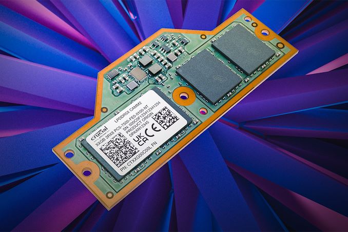
As LPCAMM2 adoption begins, the first retail memory modules are finally starting to hit the retail market, courtesy of Micron. The memory manufacturer has begun selling their LPDDR5X-based LPCAMM2 memory modules under their in-house Crucial brand, making them available on the latter's storefront. Timed to coincide with the release of Lenovo's ThinkPad P1 Gen 7 laptop – the first retail laptop designed to use the memory modules – this marks the de facto start of the eagerly-awaited modular LPDDR5X memory era.
Micron's Low Power Compression Attached Memory Module 2 (LPCAMM2) modules are available in capacities of 32 GB and 64 GB. These are dual-channel modules that feature a 128-bit wide interface, and are based around LPDDR5X memory running at data rates up to 7500 MT/s. This gives a single LPCAMM2 a peak bandwidth of 120 GB/s. Micron is not disclosing the latencies of its LPCAMM2 memory modules, but it says that high data transfer rates of LPDDR5X compensate for the extended timings.
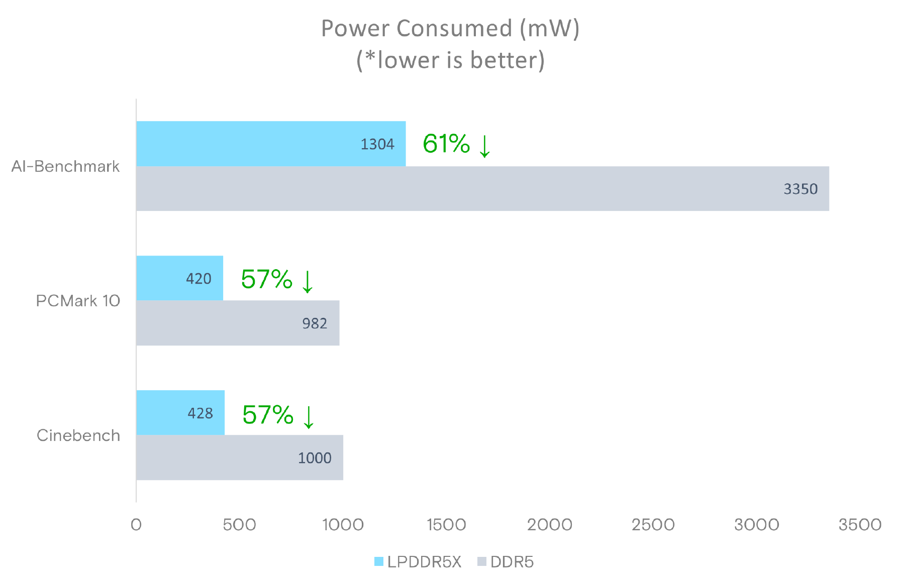
Micron says that LPDDR5X memory offers significantly lower power consumption, with active power per 64-bit bus being 43-58% lower than DDR5 at the same speed, and standby power up to 80% lower. Meanwhile, similar to DDR5 modules, LPCAMM2 modules include a power management IC and voltage regulating circuitry, which provides module manufacturers additional opportunities to reduce power consumption of their products.
Source: Micron LPDDR5X LPCAMM2 Technical Brief
It's worth noting, however, that at least for the first generation of LPCAMM2 modules, system vendors will need to pick between modularity and performance. While soldered-down LPDDR5X memory is available at speeds up to 8533 MT/sec – and with 9600 MT/sec on the horizon – the fastest LPCAMM2 modules planned for this year by both Micron and rival Samsung will be running at 7500 MT/sec. So vendors will have to choose between the flexibility of offering modular LPDDR5X, or the higher bandwidth (and space savings) offered by soldering down their memory.
Micron, for its part, is projecting that 9600 MT/sec LPCAMM2 modules will be available by 2026. Though it's all but certain that faster memory will also be avaialble in the same timeframe.
Micron's Crucial LPDDR5X 32 GB module costs $174.99, whereas a 64 GB module costs $329.99.
Memory
Lorem Ipsum is simply dummy text of the printing and typesetting industry. Lorem Ipsum has been the industry's.
While the new CAMM and LPCAMM memory modules for laptops have garnered a great deal of attention in recent months, it's not just the mobile side of the PC memory industry that is looking at changes. The desktop memory market is also coming due for some upgrades to further improve DIMM performance, in the form of a new DIMM variety called the Clocked Unbuffered DIMM (CUDIMM). And while this memory isn't in use quite yet, several memory vendors had their initial CUDIMM products on display at this year's Computex trade show, offering a glimpse into the future of desktop memory.
A variation on traditional Unbuffered DIMMs (UDIMMs), Clocked UDIMMs (and Clocked SODIMMs) have been created as another solution to the ongoing signal integrity challenges presented by DDR5 memory. DDR5 allows for rather speedy transfer rates with removable (and easily installed) DIMMs, but further performance increases are running up against the laws of physics when it comes to the electrical challenges of supporting memory on a stick – particularly with so many capacity/performance combinations like we see today. And while those challenges aren't insurmountable, if DDR5 (and eventually, DDR6) are to keep increasing in speed, some changes appear to be needed to produce more electrically robust DIMMs, which is giving rise to the CUDIMM.
Standardized by JEDEC earlier this year as JESD323, CUDIMMs tweak the traditional unbuffered DIMM by adding a clock driver (CKD) to the DIMM itself, with the tiny IC responsible for regenerating the clock signal driving the actual memory chips. By generating a clean clock locally on the DIMM (rather than directly using the clock from the CPU, as is the case today), CUDIMMs are designed to offer improved stability and reliability at high memory speeds, combating the electrical issues that would otherwise cause reliability issues at faster memory speeds. In other words, adding a clock driver is the key to keeping DDR5 operating reliably at high clockspeeds.
All told, JEDEC is proposing that CUDIMMs be used for DDR5-6400 speeds and higher, with the first version of the specification covering speeds up to DDR5-7200. The new DIMMs will also be drop-in compatible with existing platforms (at least on paper), using the same 288-pin connector as today's standard DDR5 UDIMM and allowing for a relatively smooth transition towards higher DDR5 clockspeeds.
Memory


![TSMC to Expand Specialty Capacity by 50%, Introduce 4nm N4e Low-Power Node <p align="center"><a href="https://www.anandtech.com/show/21397/tsmc-to-expand-specialty-capacity-by-50-introduce-4nm-lowpower-node"><img src="https://images.anandtech.com/doci/21397/tsmc-semiconductor-fab-wafer-1-678_575px.jpg" alt="" /></a></p><p><p>With all the new fabs being built in Germany and Japan, as well as the expansion of production capacity in China, TSMC is planning to extend its production capacity for specialty technologies by 50% by 2027. As disclosed by the company during its European Technology Symposium this week, TSMC expects to need to not only convert existing capacity to meet demands for specialty processes, but even build new (greenfield) fab space just for this purpose. One of the big drivers for this demand, in turn, will be TSMC's next specialty node: N4e, a 4nm-class ultra-low-power production node.</p>
<p>"In the past, we always did the review phase [for upcoming fabs], but for the first time in a long time at TSMC, we started building greenfield fab that will address the future specialty technology requirements," said Dr. Kevin Zhang, Senior Vice President, Business Development and Overseas Operations Office, at the event. "In the next four to five years, we actually going to grow our specialty capacity by up to 1.5x. In doing so we actually expanding the footprint of our manufacturing network to improve the resiliency of the overall fab supply chain."</p>
<p>On top of its well-known major logic nodes like N5 and N3E, TSMC also offers a suite of specialty nodes for applications such as power semiconductors, mixed analog I/O, and ultra-low-power applications (e.g. IoT). These are typically based on the company's trailing manufacturing processes, but regardless of the underlying technology, the capacity demand for these nodes is growing right alongside the demand for TSMC's major logic nodes. All of which has required TSMC to reevaluate how they go about planning for capacity on their specialty nodes.</p>
<p>TSMC's expansion strategy in the recent years has pursued several goals. One of them has been to build new fabs outside of Taiwan; another has been to generally expand production capacity to meet future demand for all types of process technologies – which is why the company is building up capacity for specialty nodes.</p>
<p>At present, TSMC's most advanced specialty node is N6e, an N7/N6 variant that supports operating voltages between 0.4V and 0.9V. With N4e, TSMC is looking at voltages below 0.4V. Though for now, TSMC is not disclosing much in the way of technical details for the planned node; given the company's history here, we expect they'll have more to talk about next year once the new process is ready.</p>
</p> Semiconductors](https://lh3.googleusercontent.com/blogger_img_proxy/AEn0k_sEmmZUljn1joFRDkHtUwAB0GgwkQBtPRX_sBxyjByy7c7MiChE9P7BeLg0kzUDhb3UBlTRHcee3mM-E6JYJKlkzqxUPkpX8nMUEoIdHJouWKeRhM-pOpx1iag7U3AiCcm7wjOA0tuxwcETsAA4w88L1KwmemKemA=w72-h72-p-k-no-nu)
 available to its members, and expects full specifications to be officially released sometime in 2025. The goal is to deliver a 128 GT/s data rate with up to 512 GBps of bidirectional traffic using x16 links. Similar to PCIe 6.0, this specification will also utilize PAM4 signaling and maintain backwards compatibility. Power efficiency as well as silicon die area are also being kept in mind as part of the drafting process.</p>
<p align="center"><a href="https://www.anandtech.com/show/21531/pcisig-demonstrates-pcie-60-interoperability-at-fms-2024"><img alt="" src="https://images.anandtech.com/doci/21531/pcie-char_575px.jpg" /></a></p>
<p>The move to PAM4 signaling brings higher bit-error rates compared to the previous NRZ scheme. This made it necessary to adopt a different error correction scheme in PCIe 6.0 - instead of operating on variable length packets, PCIe 6.0's Flow Control Unit (FLIT) encoding operates on fixed size packets to aid in forward error correction. PCIe 7.0 retains these aspects.</p>
<p>The integrators list for the PCIe 6.0 compliance program is also expected to come out in 2025, though initial testing is already in progress. This was evident by the FMS 2024 demo involving Cadence's 3nm test chip for its PCIe 6.0 IP offering along with Teledyne Lecroy's PCIe 6.0 analyzer. These timelines track well with the specification completion dates and compliance program availability for previous PCIe generations.</p>
<p align="center"><a href="https://www.anandtech.com/show/21531/pcisig-demonstrates-pcie-60-interoperability-at-fms-2024"><img alt="" src="https://images.anandtech.com/doci/21531/pcie-cadence_575px.jpg" /></a></p>
<p>We also received an update on the optical workgroup - while being optical-technology agnostic, the WG also intends to develop technology-specific form-factors including pluggable optical transceivers, on-board optics, co-packaged optics, and optical I/O. The logical and electrical layers of the PCIe 6.0 specifications are being enhanced to accommodate the new optical PCIe standardization and this process will also be done with PCIe 7.0 to coincide with that standard's release next year.</p>
<p align="center"><a href="https://www.anandtech.com/show/21531/pcisig-demonstrates-pcie-60-interoperability-at-fms-2024"><img alt="" src="https://images.anandtech.com/doci/21531/pcie-cabling_575px.jpg" /></a></p>
<p>The PCI-SIG also has ongoing cabling initiatives. On the consumer side, we have seen significant traction for Thunderbolt and external GPU enclosures. However, even datacenters and enterprise systems are moving towards cabling solutions as it becomes evident that disaggregation of components such as storage from the CPU and GPU are better for thermal design. Additionally maintaining signal integrity over longer distances becomes difficult for on-board signal traces. Cabling internal to the computing systems can help here.</p>
<p>OCuLink emerged as a good candidate and was adopted fairly widely as an internal link in server systems. It has even made an appearance in mini-PCs from some Chinese manufacturers in its external avatar for the consumer market, albeit with limited traction. As speeds increase, a widely-adopted standard for external PCIe peripherals (or even connecting components within a system) will become imperative.</p>
</p> Storage)
 available to its members, and expects full specifications to be officially released sometime in 2025. The goal is to deliver a 128 GT/s data rate with up to 512 GBps of bidirectional traffic using x16 links. Similar to PCIe 6.0, this specification will also utilize PAM4 signaling and maintain backwards compatibility. Power efficiency as well as silicon die area are also being kept in mind as part of the drafting process.</p>
<p align="center"><a href="https://www.anandtech.com/show/21531/pcisig-demonstrates-pcie-60-interoperability-at-fms-2024"><img alt="" src="https://images.anandtech.com/doci/21531/pcie-char_575px.jpg" /></a></p>
<p>The move to PAM4 signaling brings higher bit-error rates compared to the previous NRZ scheme. This made it necessary to adopt a different error correction scheme in PCIe 6.0 - instead of operating on variable length packets, PCIe 6.0's Flow Control Unit (FLIT) encoding operates on fixed size packets to aid in forward error correction. PCIe 7.0 retains these aspects.</p>
<p>The integrators list for the PCIe 6.0 compliance program is also expected to come out in 2025, though initial testing is already in progress. This was evident by the FMS 2024 demo involving Cadence's 3nm test chip for its PCIe 6.0 IP offering along with Teledyne Lecroy's PCIe 6.0 analyzer. These timelines track well with the specification completion dates and compliance program availability for previous PCIe generations.</p>
<p align="center"><a href="https://www.anandtech.com/show/21531/pcisig-demonstrates-pcie-60-interoperability-at-fms-2024"><img alt="" src="https://images.anandtech.com/doci/21531/pcie-cadence_575px.jpg" /></a></p>
<p>We also received an update on the optical workgroup - while being optical-technology agnostic, the WG also intends to develop technology-specific form-factors including pluggable optical transceivers, on-board optics, co-packaged optics, and optical I/O. The logical and electrical layers of the PCIe 6.0 specifications are being enhanced to accommodate the new optical PCIe standardization and this process will also be done with PCIe 7.0 to coincide with that standard's release next year.</p>
<p align="center"><a href="https://www.anandtech.com/show/21531/pcisig-demonstrates-pcie-60-interoperability-at-fms-2024"><img alt="" src="https://images.anandtech.com/doci/21531/pcie-cabling_575px.jpg" /></a></p>
<p>The PCI-SIG also has ongoing cabling initiatives. On the consumer side, we have seen significant traction for Thunderbolt and external GPU enclosures. However, even datacenters and enterprise systems are moving towards cabling solutions as it becomes evident that disaggregation of components such as storage from the CPU and GPU are better for thermal design. Additionally maintaining signal integrity over longer distances becomes difficult for on-board signal traces. Cabling internal to the computing systems can help here.</p>
<p>OCuLink emerged as a good candidate and was adopted fairly widely as an internal link in server systems. It has even made an appearance in mini-PCs from some Chinese manufacturers in its external avatar for the consumer market, albeit with limited traction. As speeds increase, a widely-adopted standard for external PCIe peripherals (or even connecting components within a system) will become imperative.</p>
</p> Storage | https://compbuddey.blogspot.com/2024/10/pci-sig-demonstrates-pcie-60_13.html)
 available to its members, and expects full specifications to be officially released sometime in 2025. The goal is to deliver a 128 GT/s data rate with up to 512 GBps of bidirectional traffic using x16 links. Similar to PCIe 6.0, this specification will also utilize PAM4 signaling and maintain backwards compatibility. Power efficiency as well as silicon die area are also being kept in mind as part of the drafting process.</p>
<p align="center"><a href="https://www.anandtech.com/show/21531/pcisig-demonstrates-pcie-60-interoperability-at-fms-2024"><img alt="" src="https://images.anandtech.com/doci/21531/pcie-char_575px.jpg" /></a></p>
<p>The move to PAM4 signaling brings higher bit-error rates compared to the previous NRZ scheme. This made it necessary to adopt a different error correction scheme in PCIe 6.0 - instead of operating on variable length packets, PCIe 6.0's Flow Control Unit (FLIT) encoding operates on fixed size packets to aid in forward error correction. PCIe 7.0 retains these aspects.</p>
<p>The integrators list for the PCIe 6.0 compliance program is also expected to come out in 2025, though initial testing is already in progress. This was evident by the FMS 2024 demo involving Cadence's 3nm test chip for its PCIe 6.0 IP offering along with Teledyne Lecroy's PCIe 6.0 analyzer. These timelines track well with the specification completion dates and compliance program availability for previous PCIe generations.</p>
<p align="center"><a href="https://www.anandtech.com/show/21531/pcisig-demonstrates-pcie-60-interoperability-at-fms-2024"><img alt="" src="https://images.anandtech.com/doci/21531/pcie-cadence_575px.jpg" /></a></p>
<p>We also received an update on the optical workgroup - while being optical-technology agnostic, the WG also intends to develop technology-specific form-factors including pluggable optical transceivers, on-board optics, co-packaged optics, and optical I/O. The logical and electrical layers of the PCIe 6.0 specifications are being enhanced to accommodate the new optical PCIe standardization and this process will also be done with PCIe 7.0 to coincide with that standard's release next year.</p>
<p align="center"><a href="https://www.anandtech.com/show/21531/pcisig-demonstrates-pcie-60-interoperability-at-fms-2024"><img alt="" src="https://images.anandtech.com/doci/21531/pcie-cabling_575px.jpg" /></a></p>
<p>The PCI-SIG also has ongoing cabling initiatives. On the consumer side, we have seen significant traction for Thunderbolt and external GPU enclosures. However, even datacenters and enterprise systems are moving towards cabling solutions as it becomes evident that disaggregation of components such as storage from the CPU and GPU are better for thermal design. Additionally maintaining signal integrity over longer distances becomes difficult for on-board signal traces. Cabling internal to the computing systems can help here.</p>
<p>OCuLink emerged as a good candidate and was adopted fairly widely as an internal link in server systems. It has even made an appearance in mini-PCs from some Chinese manufacturers in its external avatar for the consumer market, albeit with limited traction. As speeds increase, a widely-adopted standard for external PCIe peripherals (or even connecting components within a system) will become imperative.</p>
</p> Storage&body=https://compbuddey.blogspot.com/2024/10/pci-sig-demonstrates-pcie-60_13.html)
0 Comments