

NVIDIA on Tuesday said that future monitor scalers from MediaTek will support its G-Sync technologies. NVIDIA is partnering with MediaTek to integrate its full range of G-Sync technologies into future monitors without requiring a standalone G-Sync module, which makes advanced gaming features more accessible across a broader range of displays.
Traditionally, G-Sync technology relied on a dedicated G-sync module – based on an Altera FPGA – to handle syncing display refresh rates with the GPU in order to reduce screen tearing, stutter, and input lag. As a more basic solution, in 2019 NVIDIA introduced G-Sync Compatible certification and branding, which leveraged the industry-standard VESA AdaptiveSync technology to handle variable refresh rates. In lieu of using a dedicated module, leveraging AdaptiveSync allowed for cheaper monitors, with NVIDIA's program serving as a stamp of approval that the monitor worked with NVIDIA GPUs and met NVIDIA's performance requirements. Still, G-Sync Compatible monitors still lack some features that, to date, require the dedicated G-Sync module.
Through this new partnership with MediaTek, MediaTek will bring support for all of NVIDIA's G-Sync technologies, including the latest G-Sync Pulsar, directly into their scalers. G-Sync Pulsar enhances motion clarity and reduces ghosting, providing a smoother gaming experience. In addition to variable refresh rates and Pulsar, MediaTek-based G-Sync displays will support such features as variable overdrive, 12-bit color, Ultra Low Motion Blur, low latency HDR, and Reflex Analyzer. This integration will allow more monitors to support a full range of G-Sync features without having to incorporate an expensive FPGA.
The first monitors to feature full G-Sync support without needing an NVIDIA module include the AOC Agon Pro AG276QSG2, Acer Predator XB273U F5, and ASUS ROG Swift 360Hz PG27AQNR. These monitors offer 360Hz refresh rates, 1440p resolution, and HDR support.
What remains to be seen is which specific MediaTek's scalers will support NVIDIA's G-Sync technology – or if the company is going to implement support into all of their scalers going forward. It also remains to be seen whether monitors with NVIDIA's dedicated G-Sync modules retain any advantages over displays with MediaTek's scalers.
Monitors
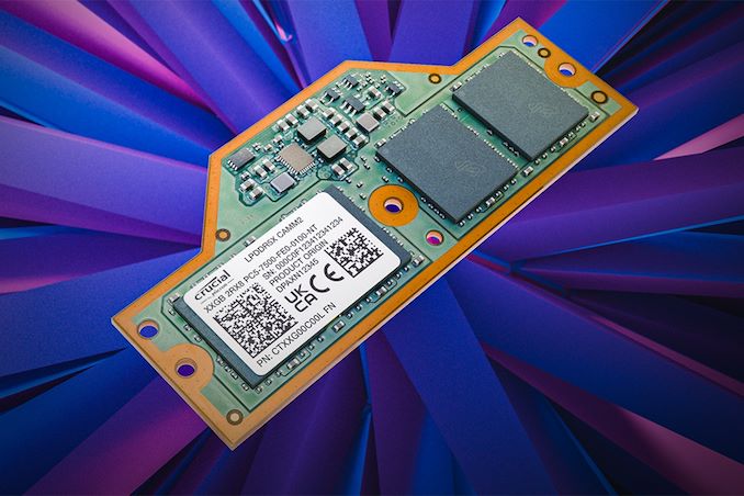
As LPCAMM2 adoption begins, the first retail memory modules are finally starting to hit the retail market, courtesy of Micron. The memory manufacturer has begun selling their LPDDR5X-based LPCAMM2 memory modules under their in-house Crucial brand, making them available on the latter's storefront. Timed to coincide with the release of Lenovo's ThinkPad P1 Gen 7 laptop – the first retail laptop designed to use the memory modules – this marks the de facto start of the eagerly-awaited modular LPDDR5X memory era.
Micron's Low Power Compression Attached Memory Module 2 (LPCAMM2) modules are available in capacities of 32 GB and 64 GB. These are dual-channel modules that feature a 128-bit wide interface, and are based around LPDDR5X memory running at data rates up to 7500 MT/s. This gives a single LPCAMM2 a peak bandwidth of 120 GB/s. Micron is not disclosing the latencies of its LPCAMM2 memory modules, but it says that high data transfer rates of LPDDR5X compensate for the extended timings.
Micron says that LPDDR5X memory offers significantly lower power consumption, with active power per 64-bit bus being 43-58% lower than DDR5 at the same speed, and standby power up to 80% lower. Meanwhile, similar to DDR5 modules, LPCAMM2 modules include a power management IC and voltage regulating circuitry, which provides module manufacturers additional opportunities to reduce power consumption of their products.
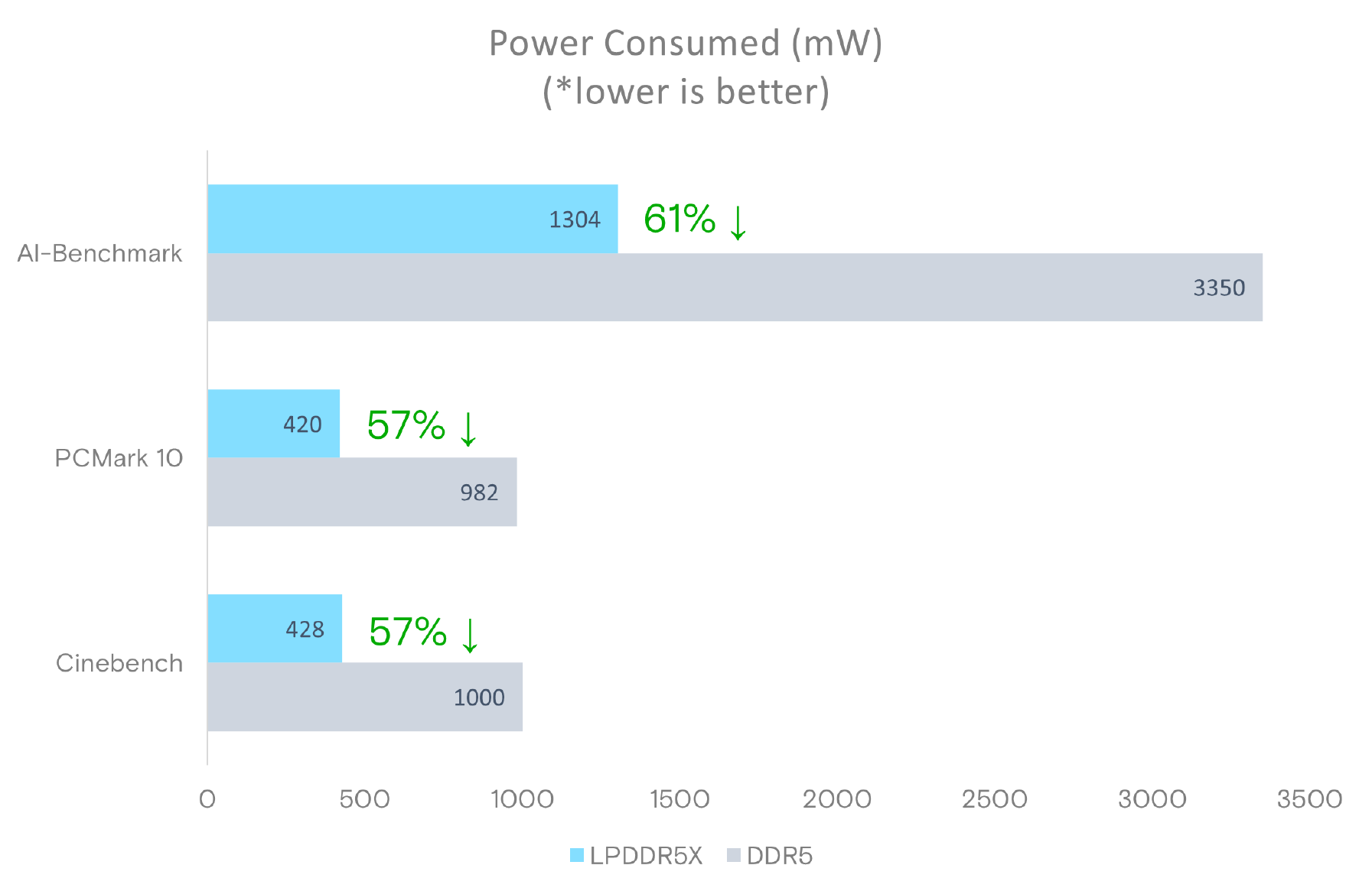
Source: Micron LPDDR5X LPCAMM2 Technical Brief
It's worth noting, however, that at least for the first generation of LPCAMM2 modules, system vendors will need to pick between modularity and performance. While soldered-down LPDDR5X memory is available at speeds up to 8533 MT/sec – and with 9600 MT/sec on the horizon – the fastest LPCAMM2 modules planned for this year by both Micron and rival Samsung will be running at 7500 MT/sec. So vendors will have to choose between the flexibility of offering modular LPDDR5X, or the higher bandwidth (and space savings) offered by soldering down their memory.
Micron, for its part, is projecting that 9600 MT/sec LPCAMM2 modules will be available by 2026. Though it's all but certain that faster memory will also be avaialble in the same timeframe.
Micron's Crucial LPDDR5X 32 GB module costs $174.99, whereas a 64 GB module costs $329.99.
Memory

A few years back, the Japanese government's New Energy and Industrial Technology Development Organization (NEDO ) allocated funding for the development of green datacenter technologies. With the aim to obtain up to 40% savings in overall power consumption, several Japanese companies have been developing an optical interface for their enterprise SSDs. And at this year's FMS, Kioxia had their optical interface on display.

For this demonstration, Kioxia took its existing CM7 enterprise SSD and created an optical interface for it. A PCIe card with on-board optics developed by Kyocera is installed in the server slot. An optical interface allows data transfer over long distances (it was 40m in the demo, but Kioxia promises lengths of up to 100m for the cable in the future). This allows the storage to be kept in a separate room with minimal cooling requirements compared to the rack with the CPUs and GPUs. Disaggregation of different server components will become an option as very high throughput interfaces such as PCIe 7.0 (with 128 GT/s rates) become available.

The demonstration of the optical SSD showed a slight loss in IOPS performance, but a significant advantage in the latency metric over the shipping enterprise SSD behind a copper network link. Obviously, there are advantages in wiring requirements and signal integrity maintenance with optical links.
Being a proof-of-concept demonstration, we do see the requirement for an industry-standard approach if this were to gain adoption among different datacenter vendors. The PCI-SIG optical workgroup will need to get its act together soon to create a standards-based approach to this problem.
Storage
As LPCAMM2 adoption begins, the first retail memory modules are finally starting to hit the retail market, courtesy of Micron. The memory manufacturer has begun selling their LPDDR5X-based LPCAMM2 memory modules under their in-house Crucial brand, making them available on the latter's storefront. Timed to coincide with the release of Lenovo's ThinkPad P1 Gen 7 laptop – the first retail laptop designed to use the memory modules – this marks the de facto start of the eagerly-awaited modular LPDDR5X memory era.
Micron's Low Power Compression Attached Memory Module 2 (LPCAMM2) modules are available in capacities of 32 GB and 64 GB. These are dual-channel modules that feature a 128-bit wide interface, and are based around LPDDR5X memory running at data rates up to 7500 MT/s. This gives a single LPCAMM2 a peak bandwidth of 120 GB/s. Micron is not disclosing the latencies of its LPCAMM2 memory modules, but it says that high data transfer rates of LPDDR5X compensate for the extended timings.
Micron says that LPDDR5X memory offers significantly lower power consumption, with active power per 64-bit bus being 43-58% lower than DDR5 at the same speed, and standby power up to 80% lower. Meanwhile, similar to DDR5 modules, LPCAMM2 modules include a power management IC and voltage regulating circuitry, which provides module manufacturers additional opportunities to reduce power consumption of their products.
Source: Micron LPDDR5X LPCAMM2 Technical Brief
It's worth noting, however, that at least for the first generation of LPCAMM2 modules, system vendors will need to pick between modularity and performance. While soldered-down LPDDR5X memory is available at speeds up to 8533 MT/sec – and with 9600 MT/sec on the horizon – the fastest LPCAMM2 modules planned for this year by both Micron and rival Samsung will be running at 7500 MT/sec. So vendors will have to choose between the flexibility of offering modular LPDDR5X, or the higher bandwidth (and space savings) offered by soldering down their memory.
Micron, for its part, is projecting that 9600 MT/sec LPCAMM2 modules will be available by 2026. Though it's all but certain that faster memory will also be avaialble in the same timeframe.
Micron's Crucial LPDDR5X 32 GB module costs $174.99, whereas a 64 GB module costs $329.99.
Memory
A few years back, the Japanese government's New Energy and Industrial Technology Development Organization (NEDO ) allocated funding for the development of green datacenter technologies. With the aim to obtain up to 40% savings in overall power consumption, several Japanese companies have been developing an optical interface for their enterprise SSDs. And at this year's FMS, Kioxia had their optical interface on display.
For this demonstration, Kioxia took its existing CM7 enterprise SSD and created an optical interface for it. A PCIe card with on-board optics developed by Kyocera is installed in the server slot. An optical interface allows data transfer over long distances (it was 40m in the demo, but Kioxia promises lengths of up to 100m for the cable in the future). This allows the storage to be kept in a separate room with minimal cooling requirements compared to the rack with the CPUs and GPUs. Disaggregation of different server components will become an option as very high throughput interfaces such as PCIe 7.0 (with 128 GT/s rates) become available.
The demonstration of the optical SSD showed a slight loss in IOPS performance, but a significant advantage in the latency metric over the shipping enterprise SSD behind a copper network link. Obviously, there are advantages in wiring requirements and signal integrity maintenance with optical links.
Being a proof-of-concept demonstration, we do see the requirement for an industry-standard approach if this were to gain adoption among different datacenter vendors. The PCI-SIG optical workgroup will need to get its act together soon to create a standards-based approach to this problem.
Storage
As Qualcomm prepares for the mid-year launch of their forthcoming Snapdragon X SoCs for PCs, and the eagerly anticipated Oryon CPU cores within, the company is finally shoring up their official product plans, and releasing some additional technical details in the process. Thus far the company has been demonstrating their Snapdragon X Elite SoC in its highest-performing, fully-enabled configuration. But the retail Snapdragon X Elite will not be a single part; instead, Qualcomm is preparing a whole range of chip configurations for various price/performance tiers in the market. Altogether, there will be 3 Snapdragon X Elite SKUs that differ in CPU and GPU performance.
As well, the company is introducing a second Snapdragon X tier, Snapdragon X Plus, for those SKUs positioned below the Elite performance tier. As of today, this will be a single configuration. But if the Snapdragon X lineup is successful and demand warrants it, I would not be surprised to see Qualcomm expand it further – as they have certainly left themselves the room for it in their product stack. In the meantime, with Qualcomm’s expected launch competition now shipping (Intel Core Ultra Meteor Lake and AMD Ryzen Mobile 8040 Hawk Point), the company is also very confident that even these reduced performance Snapdragon X Plus chips will be able to beat Intel and AMD in multithreaded performance – never mind the top-tier Snapdragon X Elite chips.
Qualcomm will be launching this expanded four chip stack at once; so both Snapdragon X Elite and Snapdragon X Plus tier devices should be available at the same time. The company’s goal is still to have devices on the shelf “mid-year”, although the company isn’t providing any more precise guidance than that. With Qualcomm’s CEO, Cristiano Amon, set to deliver a Computex keynote in June, I expect we’ll get more specific details on timings then, along with the company and its partners using the event to announce and showcase some retail laptop designs. So this is very much looking like a summer launch at the moment.
In the meantime, Qualcomm is already showing off what their Snapdragon X Plus chips can do with a fresh set of live benchmarks, akin to their Snapdragon X Elite performance previews from October 2023. We’ll dive into those in a bit, but suffice it to say, Qualcomm knows the score, and they want to make sure the entire world knows when they’re winning.
CPUs
![]()
In addition to revealing its roadmap and plans concerning its current leading-edge process technologies, TSMC also shared progress of its N2 node as part of its Symposiums 2024. The company's first 2nm-class fabrication node, and predominantly featuring gate-all-around transistors, according to TSMC N2 has almost achieved its target performance and yield goals, which places it on track to enter high-volume manufacturing in the second half of 2025.
TSMC states that 'N2 development is well on track and N2P is next.' In particular, gate-all-around nanosheet devices currently achieve over 90% of their expected performance, whereas yields of 256 Mb SRAM (32 MB) devices already exceeds 80%, depending on the batch. All of this for a node that is over a year away from mass production.
Meanwhile, average yield of a 256 Mb SRAM was around 70% as of March, 2024, up from around 35% in April, 2023. Device performance has also been improving with higher frequencies being achieved while keeping power consumption in check.
Chip designer interest towards TSMC's first 2nm-class gate-all-around nanosheet transistor-based technology is significant, too. The number of new tape-outs (NTOs) in the first year of N2 is over two-times higher than it was for N5. Though with that said, given TSMC's close working relationship with a handful of high-volume vendors – most notably Appe – NTOs can be a very misleading figure since the first year of a new node at TSMC is capacity constrained, and consequently the bulk of that capacity goes to TSMC's priority partners.
Meanwhile, there were considerably more N5 tapeouts in its second year (some where N5P, of course) and N2 promises to have 2.6X more NTOs in its second year. So the node indeed looks quite promising. In fact, based on TSMC's slides (which we're unfortunately not able to republish), N2 is more popular than N3 in terms of NTOs both in the first and the second years of existence.
When it comes to the second year of N2, in the second half of 2026 TSMC plans to roll out its N2P technology, which promises additional performance and power benefits. N2P is expected to improve frequency by 15% - 20%, reduce power consumption by 30% - 40%, and increase chip density by over 1.15 times compared to N3E, significant benefits to move to all-new GAA nanosheet transistors.
Finally, for those companies that need the best in performance, power, and density, TSMC is poised to offer their A16 process in 2026. That node will also bring in backside power delivery, which will add costs, but is expected to greatly improve performance efficiency and scaling.
Semiconductors
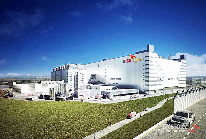
SK hynix is considering whether to build an advanced packaging facility in Indiana, reports the Wall Street Journal. If the company proceeds with the plan, it intends to invest $4 billion in it and construct one of the world's largest advanced packaging facilities. But to accomplish the project, SK hynix expects it will need help from the U.S. government.
Acknowledging the report but stopping short of confirming the company's plans, a company spokeswoman told the WSJ that SK hynix "is reviewing its advanced chip packaging investment in the U.S., but hasn’t made a final decision yet."
Companies like TSMC and Intel spend billions on advanced packaging facilities, but so far, no company has announced a chip packaging plant worth quite as much as SH hynix's $4 billion. The field of advanced packaging – CoWoS, passive silicon interposers, redistribution layers, die-to-die bonding, and other cutting edge technologies – has seen an explosion in demand in the last half-decade. As bandwidth advances with traditional organic packaging are largely played out, chip designers have needed to turn to more complex (and difficult to assemble) technologies in order to wire up an ever larger number of signals at ever-higher transfer rates. Which has turned advanced packaging into a bottleneck for high-end chip and accelerator production, driving a need for additional packaging facilities.
If SK hynix approves the project, the advanced packaging facility is expected to begin operations in 2028 and could create as many as 1,000 jobs. With an estimated cost of $4 billion, the plant is poised to become one of the largest advanced packaging facilities in the world.
Meanwhile, government backing is thought to be essential for investments of this scale, with potential state and federal tax incentives, according to the report. These incentives form part of a broader initiative to bolster the U.S. semiconductor industry and decrease dependence on memory produced in South Korea.
SK hynix is the world's leading producer of HBM memory, and is one of the key HBM suppliers to NVIDIA. Next generations of HBM memory (including HBM4 and HBM4E) will require even closer collaboration between chip designers, chipmakers, and memory makers. Therefore, packaging HBM in America could be a significant benefit for NVIDIA, AMD, and other U.S. chipmakers.
Investing in the Indiana facility will be a strategic move by SK hynix to enhance its advanced chip packaging capabilities in general and demonstrating dedication to the U.S. semiconductor industry.
Memory
Lorem Ipsum is simply dummy text of the printing and typesetting industry. Lorem Ipsum has been the industry's.
As LPCAMM2 adoption begins, the first retail memory modules are finally starting to hit the retail market, courtesy of Micron. The memory manufacturer has begun selling their LPDDR5X-based LPCAMM2 memory modules under their in-house Crucial brand, making them available on the latter's storefront. Timed to coincide with the release of Lenovo's ThinkPad P1 Gen 7 laptop – the first retail laptop designed to use the memory modules – this marks the de facto start of the eagerly-awaited modular LPDDR5X memory era.
Micron's Low Power Compression Attached Memory Module 2 (LPCAMM2) modules are available in capacities of 32 GB and 64 GB. These are dual-channel modules that feature a 128-bit wide interface, and are based around LPDDR5X memory running at data rates up to 7500 MT/s. This gives a single LPCAMM2 a peak bandwidth of 120 GB/s. Micron is not disclosing the latencies of its LPCAMM2 memory modules, but it says that high data transfer rates of LPDDR5X compensate for the extended timings.
Micron says that LPDDR5X memory offers significantly lower power consumption, with active power per 64-bit bus being 43-58% lower than DDR5 at the same speed, and standby power up to 80% lower. Meanwhile, similar to DDR5 modules, LPCAMM2 modules include a power management IC and voltage regulating circuitry, which provides module manufacturers additional opportunities to reduce power consumption of their products.
Source: Micron LPDDR5X LPCAMM2 Technical Brief
It's worth noting, however, that at least for the first generation of LPCAMM2 modules, system vendors will need to pick between modularity and performance. While soldered-down LPDDR5X memory is available at speeds up to 8533 MT/sec – and with 9600 MT/sec on the horizon – the fastest LPCAMM2 modules planned for this year by both Micron and rival Samsung will be running at 7500 MT/sec. So vendors will have to choose between the flexibility of offering modular LPDDR5X, or the higher bandwidth (and space savings) offered by soldering down their memory.
Micron, for its part, is projecting that 9600 MT/sec LPCAMM2 modules will be available by 2026. Though it's all but certain that faster memory will also be avaialble in the same timeframe.
Micron's Crucial LPDDR5X 32 GB module costs $174.99, whereas a 64 GB module costs $329.99.
Memory
A few years back, the Japanese government's New Energy and Industrial Technology Development Organization (NEDO ) allocated funding for the development of green datacenter technologies. With the aim to obtain up to 40% savings in overall power consumption, several Japanese companies have been developing an optical interface for their enterprise SSDs. And at this year's FMS, Kioxia had their optical interface on display.
For this demonstration, Kioxia took its existing CM7 enterprise SSD and created an optical interface for it. A PCIe card with on-board optics developed by Kyocera is installed in the server slot. An optical interface allows data transfer over long distances (it was 40m in the demo, but Kioxia promises lengths of up to 100m for the cable in the future). This allows the storage to be kept in a separate room with minimal cooling requirements compared to the rack with the CPUs and GPUs. Disaggregation of different server components will become an option as very high throughput interfaces such as PCIe 7.0 (with 128 GT/s rates) become available.
The demonstration of the optical SSD showed a slight loss in IOPS performance, but a significant advantage in the latency metric over the shipping enterprise SSD behind a copper network link. Obviously, there are advantages in wiring requirements and signal integrity maintenance with optical links.
Being a proof-of-concept demonstration, we do see the requirement for an industry-standard approach if this were to gain adoption among different datacenter vendors. The PCI-SIG optical workgroup will need to get its act together soon to create a standards-based approach to this problem.
Storage


0 Comments