

A few years back, the Japanese government's New Energy and Industrial Technology Development Organization (NEDO ) allocated funding for the development of green datacenter technologies. With the aim to obtain up to 40% savings in overall power consumption, several Japanese companies have been developing an optical interface for their enterprise SSDs. And at this year's FMS, Kioxia had their optical interface on display.

For this demonstration, Kioxia took its existing CM7 enterprise SSD and created an optical interface for it. A PCIe card with on-board optics developed by Kyocera is installed in the server slot. An optical interface allows data transfer over long distances (it was 40m in the demo, but Kioxia promises lengths of up to 100m for the cable in the future). This allows the storage to be kept in a separate room with minimal cooling requirements compared to the rack with the CPUs and GPUs. Disaggregation of different server components will become an option as very high throughput interfaces such as PCIe 7.0 (with 128 GT/s rates) become available.

The demonstration of the optical SSD showed a slight loss in IOPS performance, but a significant advantage in the latency metric over the shipping enterprise SSD behind a copper network link. Obviously, there are advantages in wiring requirements and signal integrity maintenance with optical links.
Being a proof-of-concept demonstration, we do see the requirement for an industry-standard approach if this were to gain adoption among different datacenter vendors. The PCI-SIG optical workgroup will need to get its act together soon to create a standards-based approach to this problem.
Storage
Further to our last piece which we detailed Intel's issue to motherboard vendors to follow with stock power settings for Intel's 14th and 13th Gen Core series processors, Intel has now issued a follow-up statement to this. Over the last week or so, motherboard vendors quickly released firmware updates with a new profile called 'Intel Baseline', which motherboard vendors assumed would address the instability issues.
As it turns out, Intel doesn't seem to accept this as technically, these Intel Baseline profiles are not to be confused with Intel's default specifications. This means that Intel's Baseline profiles seemingly give the impression that they are operating at default settings, hence the terminology 'baseline' used, but this still opens motherboard vendors to use their interpretations of MCE or Multi-Core Enhancement.
To clarify things for consumers, Intel has sent us the following statement:
Several motherboard manufacturers have released BIOS profiles labeled ‘Intel Baseline Profile’. However, these BIOS profiles are not the same as the 'Intel Default Settings' recommendations that Intel has recently shared with its partners regarding the instability issues reported on 13th and 14th gen K SKU processors.
These ‘Intel Baseline Profile’ BIOS settings appear to be based on power delivery guidance previously provided by Intel to manufacturers describing the various power delivery options for 13th and 14th Generation K SKU processors based on motherboard capabilities.
Intel is not recommending motherboard manufacturers to use ‘baseline’ power delivery settings on boards capable of higher values.
Intel’s recommended ‘Intel Default Settings’ are a combination of thermal and power delivery features along with a selection of possible power delivery profiles based on motherboard capabilities.
Intel recommends customers to implement the highest power delivery profile compatible with each individual motherboard design as noted in the table below:
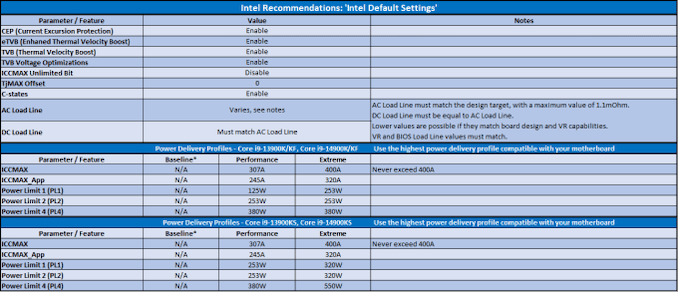
Click to Enlarge Intel's Default Settings
What Intel's statement is effectively saying to consumers, is that users shouldn't be using the Baseline Power Delivery profiles which are offered by motherboard vendors through a plethora of firmware updates. Instead, Intel is recommending users opt for Intel Default Settings, which follows what the specific processor is rated for by Intel out of the box to achieve the clock speeds advertised, without users having to worry about firmware 'over' optimization which can cause instability as there have been many reports of happening.
Not only this, but the Intel Default settings offer a combination of thermal specifications and power capabilities, including voltage and frequency curve settings that apply to the capability of the motherboard used, and the power delivery equipped on the motherboard. At least for the most part, Intel is recommending users with 14th and 13th-Gen Core series K, KF, and KS SKUs that they do not recommend users opt in using the Baseline profiles offered by motherboard vendors.
Digesting the contrast between the two statements, the key differential is that Intel's priority is reducing the current going through the processor, which for both the 14th and 13th Gen Core series processors is a maximum of 400 A, even when using the Extreme profile. We know those motherboard vendors on their Z790 and Z690 motherboards opt for an unrestricted power profile, which is essentially 'unlimited' power and current to maximize performance at the cost of power consumption and heat, which does exacerbate problems and can lead to frequent bouts of instability, especially on high-intensity workloads.
Another variable Intel is recommending is that the AC Load Line must match the design target of the processor, with a maximum value of 1.1 mOhm, and that the DC Load Line must be ... CPUs

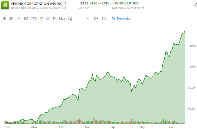
Thanks to the success of the burgeoning market for AI accelerators, NVIDIA has been on a tear this year. And the only place that’s even more apparent than the company’s rapidly growing revenues is in the company’s stock price and market capitalization. After breaking into the top 5 most valuable companies only earlier this year, NVIDIA has reached the apex of Wall Street, closing out today as the world’s most valuable company.
With a closing price of $135.58 on a day that saw NVIDIA’s stock pop up another 3.5%, NVIDIA has topped both Microsoft and Apple in valuation, reaching a market capitalization of $3.335 trillion. This follows a rapid rise in the company’s stock price, which has increased by 47% in the last month alone – particularly on the back of NVIDIA’s most recent estimates-beating earnings report – as well as a recent 10-for-1 stock split. And looking at the company’s performance over a longer time period, NVIDIA’s stock jumped a staggering 218% over the last year, or a mere 3,474% over the last 5 years.
NVIDIA’s ascension continues a trend over the last several years of tech companies all holding the top spots in the market capitalization rankings. Though this is the first time in quite a while that the traditional tech leaders of Apple and Microsoft have been pushed aside.
| Market Capitalization Rankings | ||
| Market Cap | Stock Price | |
| NVIDIA | $3.335T | $135.58 |
| Microsoft | $3.317T | $446.34 |
| Apple | $3.285T | $214.29 |
| Alphabet | $2.170T | $176.45 |
| Amazon | $1.902T | $182.81 |
Driving the rapid growth of NVIDIA and its market capitalization has been demand for AI accelerators from NVIDIA, particularly the company’s server-grade H100, H200, and GH200 accelerators for AI training. As the demand for these products has spiked, NVIDIA has been scaling up accordingly, repeatedly beating market expectations for how many of the accelerators they can ship – and what price they can charge. And despite all that growth, orders for NVIDIA’s high-end accelerators are still backlogged, underscoring how NVIDIA still isn’t meeting the full demands of hyperscalers and other enterprises.
Consequently, NVIDIA’s stock price and market capitalization have been on a tear on the basis of these future expectations. With a price-to-earnings (P/E) ratio of 76.7 – more than twice that of Microsoft or Apple – NVIDIA is priced more like a start-up than a 30-year-old tech company. But then it goes without saying that most 30-year-old tech companies aren’t tripling their revenue in a single year, placing NVIDIA in a rather unique situation at this time.
Like the stock market itself, market capitalizations are highly volatile. And historically speaking, it’s far from guaranteed that NVIDIA will be able to hold the top spot for long, never mind day-to-day fluctuations. NVIDIA, Apple, and Microsoft’s valuations are all within $50 billion (1.%) of each other, so for the moment at least, it’s still a tight race between all three companies. But no matter what happens from here, NVIDIA gets the exceptionally rare claim of having been the most valuable company in the world at some point.
(Carousel image courtesy MSN Money)
GPUs

Kioxia's booth at FMS 2024 was a busy one with multiple technology demonstrations keeping visitors occupied. A walk-through of the BiCS 8 manufacturing process was the first to grab my attention. Kioxia and Western Digital announced the sampling of BiCS 8 in March 2023. We had touched briefly upon its CMOS Bonded Array (CBA) scheme in our coverage of Kioxial's 2Tb QLC NAND device and coverage of Western Digital's 128 TB QLC enterprise SSD proof-of-concept demonstration. At Kioxia's booth, we got more insights.

Traditionally, fabrication of flash chips involved placement of the associate logic circuitry (CMOS process) around the periphery of the flash array. The process then moved on to putting the CMOS under the cell array, but the wafer development process was serialized with the CMOS logic getting fabricated first followed by the cell array on top. However, this has some challenges because the cell array requires a high-temperature processing step to ensure higher reliability that can be detrimental to the health of the CMOS logic. Thanks to recent advancements in wafer bonding techniques, the new CBA process allows the CMOS wafer and cell array wafer to be processed independently in parallel and then pieced together, as shown in the models above.

The BiCS 8 3D NAND incorporates 218 layers, compared to 112 layers in BiCS 5 and 162 layers in BiCS 6. The company decided to skip over BiCS 7 (or, rather, it was probably a short-lived generation meant as an internal test vehicle). The generation retains the four-plane charge trap structure of BiCS 6. In its TLC avatar, it is available as a 1 Tbit device. The QLC version is available in two capacities - 1 Tbit and 2 Tbit.
Kioxia also noted that while the number of layers (218) doesn't compare favorably with the latest layer counts from the competition, its lateral scaling / cell shrinkage has enabled it to be competitive in terms of bit density as well as operating speeds (3200 MT/s). For reference, the latest shipping NAND from Micron - the G9 - has 276 layers with a bit density in TLC mode of 21 Gbit/mm2, and operates at up to 3600 MT/s. However, its 232L NAND operates only up to 2400 MT/s and has a bit density of 14.6 Gbit/mm2.
It must be noted that the CBA hybrid bonding process has advantages over the current processes used by other vendors - including Micron's CMOS under array (CuA) and SK hynix's 4D PUC (periphery-under-chip) developed in the late 2010s. It is expected that other NAND vendors will also move eventually to some variant of the hybrid bonding scheme used by Kioxia.
Storage
Further to our last piece which we detailed Intel's issue to motherboard vendors to follow with stock power settings for Intel's 14th and 13th Gen Core series processors, Intel has now issued a follow-up statement to this. Over the last week or so, motherboard vendors quickly released firmware updates with a new profile called 'Intel Baseline', which motherboard vendors assumed would address the instability issues.
As it turns out, Intel doesn't seem to accept this as technically, these Intel Baseline profiles are not to be confused with Intel's default specifications. This means that Intel's Baseline profiles seemingly give the impression that they are operating at default settings, hence the terminology 'baseline' used, but this still opens motherboard vendors to use their interpretations of MCE or Multi-Core Enhancement.
To clarify things for consumers, Intel has sent us the following statement:
Several motherboard manufacturers have released BIOS profiles labeled ‘Intel Baseline Profile’. However, these BIOS profiles are not the same as the 'Intel Default Settings' recommendations that Intel has recently shared with its partners regarding the instability issues reported on 13th and 14th gen K SKU processors.
These ‘Intel Baseline Profile’ BIOS settings appear to be based on power delivery guidance previously provided by Intel to manufacturers describing the various power delivery options for 13th and 14th Generation K SKU processors based on motherboard capabilities.
Intel is not recommending motherboard manufacturers to use ‘baseline’ power delivery settings on boards capable of higher values.
Intel’s recommended ‘Intel Default Settings’ are a combination of thermal and power delivery features along with a selection of possible power delivery profiles based on motherboard capabilities.
Intel recommends customers to implement the highest power delivery profile compatible with each individual motherboard design as noted in the table below:
Click to Enlarge Intel's Default Settings
What Intel's statement is effectively saying to consumers, is that users shouldn't be using the Baseline Power Delivery profiles which are offered by motherboard vendors through a plethora of firmware updates. Instead, Intel is recommending users opt for Intel Default Settings, which follows what the specific processor is rated for by Intel out of the box to achieve the clock speeds advertised, without users having to worry about firmware 'over' optimization which can cause instability as there have been many reports of happening.
Not only this, but the Intel Default settings offer a combination of thermal specifications and power capabilities, including voltage and frequency curve settings that apply to the capability of the motherboard used, and the power delivery equipped on the motherboard. At least for the most part, Intel is recommending users with 14th and 13th-Gen Core series K, KF, and KS SKUs that they do not recommend users opt in using the Baseline profiles offered by motherboard vendors.
Digesting the contrast between the two statements, the key differential is that Intel's priority is reducing the current going through the processor, which for both the 14th and 13th Gen Core series processors is a maximum of 400 A, even when using the Extreme profile. We know those motherboard vendors on their Z790 and Z690 motherboards opt for an unrestricted power profile, which is essentially 'unlimited' power and current to maximize performance at the cost of power consumption and heat, which does exacerbate problems and can lead to frequent bouts of instability, especially on high-intensity workloads.
Another variable Intel is recommending is that the AC Load Line must match the design target of the processor, with a maximum value of 1.1 mOhm, and that the DC Load Line must be ... CPUs
Thanks to the success of the burgeoning market for AI accelerators, NVIDIA has been on a tear this year. And the only place that’s even more apparent than the company’s rapidly growing revenues is in the company’s stock price and market capitalization. After breaking into the top 5 most valuable companies only earlier this year, NVIDIA has reached the apex of Wall Street, closing out today as the world’s most valuable company.
With a closing price of $135.58 on a day that saw NVIDIA’s stock pop up another 3.5%, NVIDIA has topped both Microsoft and Apple in valuation, reaching a market capitalization of $3.335 trillion. This follows a rapid rise in the company’s stock price, which has increased by 47% in the last month alone – particularly on the back of NVIDIA’s most recent estimates-beating earnings report – as well as a recent 10-for-1 stock split. And looking at the company’s performance over a longer time period, NVIDIA’s stock jumped a staggering 218% over the last year, or a mere 3,474% over the last 5 years.
NVIDIA’s ascension continues a trend over the last several years of tech companies all holding the top spots in the market capitalization rankings. Though this is the first time in quite a while that the traditional tech leaders of Apple and Microsoft have been pushed aside.
| Market Capitalization Rankings | ||
| Market Cap | Stock Price | |
| NVIDIA | $3.335T | $135.58 |
| Microsoft | $3.317T | $446.34 |
| Apple | $3.285T | $214.29 |
| Alphabet | $2.170T | $176.45 |
| Amazon | $1.902T | $182.81 |
Driving the rapid growth of NVIDIA and its market capitalization has been demand for AI accelerators from NVIDIA, particularly the company’s server-grade H100, H200, and GH200 accelerators for AI training. As the demand for these products has spiked, NVIDIA has been scaling up accordingly, repeatedly beating market expectations for how many of the accelerators they can ship – and what price they can charge. And despite all that growth, orders for NVIDIA’s high-end accelerators are still backlogged, underscoring how NVIDIA still isn’t meeting the full demands of hyperscalers and other enterprises.
Consequently, NVIDIA’s stock price and market capitalization have been on a tear on the basis of these future expectations. With a price-to-earnings (P/E) ratio of 76.7 – more than twice that of Microsoft or Apple – NVIDIA is priced more like a start-up than a 30-year-old tech company. But then it goes without saying that most 30-year-old tech companies aren’t tripling their revenue in a single year, placing NVIDIA in a rather unique situation at this time.
Like the stock market itself, market capitalizations are highly volatile. And historically speaking, it’s far from guaranteed that NVIDIA will be able to hold the top spot for long, never mind day-to-day fluctuations. NVIDIA, Apple, and Microsoft’s valuations are all within $50 billion (1.%) of each other, so for the moment at least, it’s still a tight race between all three companies. But no matter what happens from here, NVIDIA gets the exceptionally rare claim of having been the most valuable company in the world at some point.
(Carousel image courtesy MSN Money)
GPUs
Kioxia's booth at FMS 2024 was a busy one with multiple technology demonstrations keeping visitors occupied. A walk-through of the BiCS 8 manufacturing process was the first to grab my attention. Kioxia and Western Digital announced the sampling of BiCS 8 in March 2023. We had touched briefly upon its CMOS Bonded Array (CBA) scheme in our coverage of Kioxial's 2Tb QLC NAND device and coverage of Western Digital's 128 TB QLC enterprise SSD proof-of-concept demonstration. At Kioxia's booth, we got more insights.
Traditionally, fabrication of flash chips involved placement of the associate logic circuitry (CMOS process) around the periphery of the flash array. The process then moved on to putting the CMOS under the cell array, but the wafer development process was serialized with the CMOS logic getting fabricated first followed by the cell array on top. However, this has some challenges because the cell array requires a high-temperature processing step to ensure higher reliability that can be detrimental to the health of the CMOS logic. Thanks to recent advancements in wafer bonding techniques, the new CBA process allows the CMOS wafer and cell array wafer to be processed independently in parallel and then pieced together, as shown in the models above.
The BiCS 8 3D NAND incorporates 218 layers, compared to 112 layers in BiCS 5 and 162 layers in BiCS 6. The company decided to skip over BiCS 7 (or, rather, it was probably a short-lived generation meant as an internal test vehicle). The generation retains the four-plane charge trap structure of BiCS 6. In its TLC avatar, it is available as a 1 Tbit device. The QLC version is available in two capacities - 1 Tbit and 2 Tbit.
Kioxia also noted that while the number of layers (218) doesn't compare favorably with the latest layer counts from the competition, its lateral scaling / cell shrinkage has enabled it to be competitive in terms of bit density as well as operating speeds (3200 MT/s). For reference, the latest shipping NAND from Micron - the G9 - has 276 layers with a bit density in TLC mode of 21 Gbit/mm2, and operates at up to 3600 MT/s. However, its 232L NAND operates only up to 2400 MT/s and has a bit density of 14.6 Gbit/mm2.
It must be noted that the CBA hybrid bonding process has advantages over the current processes used by other vendors - including Micron's CMOS under array (CuA) and SK hynix's 4D PUC (periphery-under-chip) developed in the late 2010s. It is expected that other NAND vendors will also move eventually to some variant of the hybrid bonding scheme used by Kioxia.
Storage
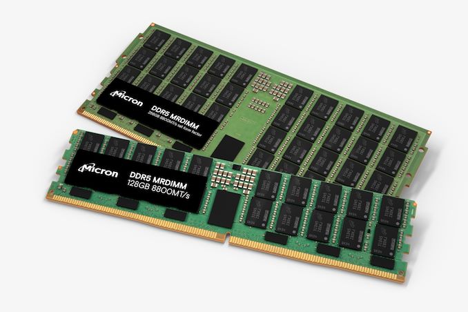
Following a relative lull in the desktop memory industry in the previous decade, the past few years have seen a flurry of new memory standards and form factors enter development. Joining the traditional DIMM/SO-DIMM form factors, we've seen the introduction of space-efficient DDR5 CAMM2s, their LPDDR5-based counterpart the LPCAMM2, and the high-clockspeed optimized CUDIMM. But JEDEC, the industry organization behind these efforts, is not done there. In a press release sent out at the start of the week, the group announced that it is working on standards for DDR5 Multiplexed Rank DIMMs (MRDIMM) for servers, as well as an updated LPCAMM standard to go with next-generation LPDDR6 memory.
Just last week Micron introduced the industry's first DDR5 MRDIMMs, which are timed to launch alongside Intel's Xeon 6 server platforms. But while Intel and its partners are moving full steam ahead on MRDIMMs, the MRDIMM specification has not been fully ratified by JEDEC itself. All told, it's not unusual to see Intel pushing the envelope here on new memory technologies (the company is big enough to bootstrap its own ecosystem). But as MRDIMMs are ultimately meant to be more than just a tool for Intel, a proper industry standard is still needed – even if that takes a bit longer.
Under the hood, MRDIMMs continue to use DDR5 components, form-factor, pinout, SPD, power management ICs (PMICs), and thermal sensors. The major change with the technology is the introduction of multiplexing, which combines multiple data signals over a single channel. The MRDIMM standard also adds RCD/DB logic in a bid to boost performance, increase capacity of memory modules up to 256 GB (for now), shrink latencies, and reduce power consumption of high-end memory subsystems. And, perhaps key to MRDIMM adoption, the standard is being implemented as a backwards-compatible extension to traditional DDR5 RDIMMs, meaning that MRDIMM-capable servers can use either RDIMMs or MRDIMMs, depending on how the operator opts to configure the system.
The MRDIMM standard aims to double the peak bandwidth to 12.8 Gbps, increasing pin speed and supporting more than two ranks. Additionally, a "Tall MRDIMM" form factor is in the works (and pictured above), which is designed to allow for higher capacity DIMMs by providing more area for laying down memory chips. Currently, ultra high capacity DIMMs require using expensive, multi-layer DRAM packages that use through-silicon vias (3DS packaging) to attach the individual DRAM dies; a Tall MRDIMM, on the other hand, can just use a larger number of commodity DRAM chips. Overall, the Tall MRDIMM form factor enables twice the number of DRAM single-die packages on the DIMM.
Meanwhile, this week's announcement from JEDEC offers the first significant insight into what to expect from LPDDR6 CAMMs. And despite LPDDR5 CAMMs having barely made it out the door, some significant shifts with LPDDR6 itself means that JEDEC will need to make some major changes to the CAMM standard to accommodate the newer memory type.
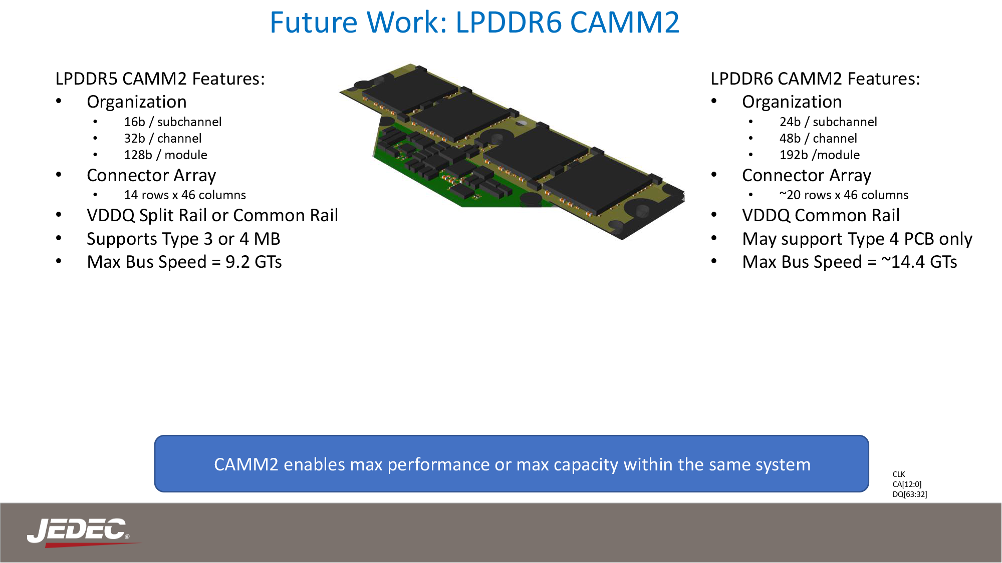
JEDEC Presentation: The CAMM2 Journey and Future Potential
Besides the higher memory clockspeeds allowed by LPDDR6 – JEDEC is targeting data transfer rates of 14.4 GT/s and higher – the new memory form-factor will also incorporate an altogether new connector array. This is to accommodate LPDDR6's wider memory bus, which sees the channel width of an individual memory chip grow from 16-bits wide to 24-bits wide. As a result, the current LPCAMM design, which is intended to match the PC standard of a cumulative 128-bit (16x8) design needs to be reconfigured to match LPDDR6's alterations.
Ultimately, JEDEC is targeting a 24-bit subhannel/48-bit channel design, which will result in a 192-bit wide LPCAMM. While the LPCAMM connector itself is set to grow from 14 rows of pins to possibly as high as 20. New memory technologies typically require new DIMMs to begin with, so it's important to clarify that this is not unexpected, but at th... Memory
Kioxia's booth at FMS 2024 was a busy one with multiple technology demonstrations keeping visitors occupied. A walk-through of the BiCS 8 manufacturing process was the first to grab my attention. Kioxia and Western Digital announced the sampling of BiCS 8 in March 2023. We had touched briefly upon its CMOS Bonded Array (CBA) scheme in our coverage of Kioxial's 2Tb QLC NAND device and coverage of Western Digital's 128 TB QLC enterprise SSD proof-of-concept demonstration. At Kioxia's booth, we got more insights.
Traditionally, fabrication of flash chips involved placement of the associate logic circuitry (CMOS process) around the periphery of the flash array. The process then moved on to putting the CMOS under the cell array, but the wafer development process was serialized with the CMOS logic getting fabricated first followed by the cell array on top. However, this has some challenges because the cell array requires a high-temperature processing step to ensure higher reliability that can be detrimental to the health of the CMOS logic. Thanks to recent advancements in wafer bonding techniques, the new CBA process allows the CMOS wafer and cell array wafer to be processed independently in parallel and then pieced together, as shown in the models above.
The BiCS 8 3D NAND incorporates 218 layers, compared to 112 layers in BiCS 5 and 162 layers in BiCS 6. The company decided to skip over BiCS 7 (or, rather, it was probably a short-lived generation meant as an internal test vehicle). The generation retains the four-plane charge trap structure of BiCS 6. In its TLC avatar, it is available as a 1 Tbit device. The QLC version is available in two capacities - 1 Tbit and 2 Tbit.
Kioxia also noted that while the number of layers (218) doesn't compare favorably with the latest layer counts from the competition, its lateral scaling / cell shrinkage has enabled it to be competitive in terms of bit density as well as operating speeds (3200 MT/s). For reference, the latest shipping NAND from Micron - the G9 - has 276 layers with a bit density in TLC mode of 21 Gbit/mm2, and operates at up to 3600 MT/s. However, its 232L NAND operates only up to 2400 MT/s and has a bit density of 14.6 Gbit/mm2.
It must be noted that the CBA hybrid bonding process has advantages over the current processes used by other vendors - including Micron's CMOS under array (CuA) and SK hynix's 4D PUC (periphery-under-chip) developed in the late 2010s. It is expected that other NAND vendors will also move eventually to some variant of the hybrid bonding scheme used by Kioxia.
Storage

Samsung had quietly launched its BM1743 enterprise QLC SSD last month with a hefty 61.44 TB SKU. At FMS 2024, the company had the even larger 122.88 TB version of that SSD on display, alongside a few recorded benchmarking sessions. Compared to the previous generation, the BM1743 comes with a 4.1x improvement in I/O performance, improvement in data retention, and a 45% improvement in power efficiency for sequential writes.

The 128 TB-class QLC SSD boasts of sequential read speeds of 7.5 GBps and write speeds of 3 GBps. Random reads come in at 1.6 M IOPS, while 16 KB random writes clock in at 45K IOPS. Based on the quoted random write access granularity, it appears that Samsung is using a 16 KB indirection unit (IU) to optimize flash management. This is similar to the strategy adopted by Solidigm with IUs larger than 4K in their high-capacity SSDs.
A recorded benchmark session on the company's PM9D3a 8-channel Gen 5 SSD was also on display.

The SSD family is being promoted as a mainstream option for datacenters, and boasts of sequential reads up to 12 GBps and writes up to 6.8 GBps. Random reads clock in at 2 M IOPS, and random writes at 400 K IOPS.

Available in multiple form-factors up to 32 TB (M.2 tops out at 2 TB), the drive's firmware includes optional support for flexible data placement (FDP) to help address the write amplification aspect.
The PM1753 is the current enterprise SSD flagship in Samsung's lineup. With support for 16 NAND channels and capacities up to 32 TB, this U.2 / E3.S SSD has advertised sequential read and write speeds of 14.8 GBps and 11 GBps respectively. Random reads and writes for 4 KB accesses are listed at 3.4 M and 600 K IOPS.

Samsung claims a 1.7x performance improvement and a 1.7x power efficiency improvement over the previous generation (PM1743), making this TLC SSD suitable for AI servers.
The 9th Gen. V-NAND wafer was also available for viewing, though photography was prohibited. Mass production of this flash memory began in April 2024.
Storage![TSMC Preps Cheaper 4nm N4C Process For 2025, Aiming For 8.5% Cost Reduction <p align="center"><a href="https://www.anandtech.com/show/21371/tsmc-preps-lower-cost-4nm-n4c-process-for-2025"><img src="https://images.anandtech.com/doci/21371/tsmc_semiconductor_fab12_1_678x452_575px.jpg" alt="" /></a></p><p><p>While the bulk of attention on TSMC is aimed at its leading-edge nodes, such as N3E and N2, loads of chips will continue to be made using more mature and proven process technologies for years to come. Which is why TSMC has continued to refine its existing nodes, including its current-generation 5nm-class offerings. To that end, at its North American Technology Symposium 2024, the company introduced a new, optimized 5nm-class node: N4C.</p>
<p>TSMC's N4C process belongs to the company's 5nm-class family of fab nodes and is a superset of N4P, the most advanced technology in that family. In a bid to further bring down 5nm manufacturing costs, for TSMC is implementing several changes for N4C, including rearchitecting their standard cell and SRAM cell, changing some design rules, and reducing the number of masking layers. As a result of these improvements, the company expects N4C to achieve both smaller die sizes as well as a reduction in production complexity, which in turn will bring die costs down by up to 8.5%. Furthermore, with the same wafer-level defect density rate as N4P, N4C stands to offer even higher functional yields thanks to its die area reduction.</p>
<p>"So, we are not done with our 5nm and 4nm [technologies]," said Kevin Zhang, Vice President of Business Development at TSMC. "From N5 to N4, we have achieved 4% density improvement optical shrink, and we continue to enhance the transistor performance. Now we bring in N4C to our 4 nm technology portfolio. N4C allows our customers to reduce their costs by remove some of the masks and to also improve on the original IP design like a standard cell and SRAM to further reduce the overall product level cost of ownership."</p>
<p style="text-align: center;"><a href="https://www.anandtech.com/show/21371/tsmc-preps-lower-cost-4nm-n4c-process-for-2025"><img alt="" src="https://images.anandtech.com/doci/21371/tsmc-n4c.png" style="width: 100%;" /></a></p>
<p>TSMC says that N4C can use the same design infrastructure as N4P, though it is unclear whether N5 and N4P IP can be re-used for N4C-based chips. Meanwhile, TSMC indicates that it offers various options for chipmakers to find the right balance between cost benefits and design effort, so companies interested in adopting a 4nm-class process technologies could well adopt N4C.</p>
<p>The development of N4C comes as many of TSMC's chip design customers are preparing to launch chips based on the company's final generation of FinFET process technology, the 3nm N3 series. While N3 is expected to be a successful family, the high costs of N3B have been an issue, and the generation is marked by diminishing performance and transistor density returns altogether. Consequently, N4C could well become a major, long-lived node at TSMC, serving as a good fit for customers who want to stick to a more cost-effective FinFET node.</p>
<p>"This is a very significant enhancement, we are working with our customer, basically to extract more value from their 4 nm investment," Zhang said.</p>
<p>TSMC expects to start volume production of N4C chips some time next year. And with TSMC having produced 5nm-class for nearly half a decade at that point, N4C should be able to hit the ground running in terms of volume and yields.</p>
<h3><strong>Related Reading</strong></h3>
<ul>
<li><a href="https://www.anandtech.com/show/21369/tsmcs-16nm-technology-announced-for-late-2026-a16-with-super-power-rail-bspdn">TSMC's 1.6nm Technology Announced for Late 2026: A16 with "Super Power Rail" Backside Power</a></li>
<li><a href="https://www.anandtech.com/show/21370/tsmc-2nm-update-n2-in-2025-n2p-loses-bspdn-nanoflex-optimizations">TSMC 2nm Update: N2 In 2025, N2P Loses Backside Power, and NanoFlex Brings Optimal Cells</a></li>
<li><a href="https://www.anandtech.com/show/21372/tsmcs-system-on-wafer-platform-goes-3d-cow-sow">TSMC's System-on-Wafer Platform Goes 3D: CoW-SoW Stacks Up the Chips</a></li>
<li><a href="https://www.anandtech.com/show/21373/tsmc-adds-silicon-photonics-coupe-roadmap-128tbps-on-package">TSMC Jumps Into Silicon Photonics, Lays Out Roadmap For 12.8 Tbps COUPE On-Package Interconnect</a></li>
</ul>
</p> Semiconductors](https://lh3.googleusercontent.com/blogger_img_proxy/AEn0k_v0K3AqJkO-5w7uB5N-7uDMZaZjrFnyYx9mPKEPeEMA4RPvIk4hFmC4_bJWIPdjKOAeKVwWBvtfp43T6rh_r2SWT7WozoI2ec0WJUqAYAAQ9nz9L6hV5Q66eFysXCADkAiLdEdDxlgWzagw4CT8gZfIiaLOBXfuOg=w72-h72-p-k-no-nu)
While the bulk of attention on TSMC is aimed at its leading-edge nodes, such as N3E and N2, loads of chips will continue to be made using more mature and proven process technologies for years to come. Which is why TSMC has continued to refine its existing nodes, including its current-generation 5nm-class offerings. To that end, at its North American Technology Symposium 2024, the company introduced a new, optimized 5nm-class node: N4C.
TSMC's N4C process belongs to the company's 5nm-class family of fab nodes and is a superset of N4P, the most advanced technology in that family. In a bid to further bring down 5nm manufacturing costs, for TSMC is implementing several changes for N4C, including rearchitecting their standard cell and SRAM cell, changing some design rules, and reducing the number of masking layers. As a result of these improvements, the company expects N4C to achieve both smaller die sizes as well as a reduction in production complexity, which in turn will bring die costs down by up to 8.5%. Furthermore, with the same wafer-level defect density rate as N4P, N4C stands to offer even higher functional yields thanks to its die area reduction.
"So, we are not done with our 5nm and 4nm [technologies]," said Kevin Zhang, Vice President of Business Development at TSMC. "From N5 to N4, we have achieved 4% density improvement optical shrink, and we continue to enhance the transistor performance. Now we bring in N4C to our 4 nm technology portfolio. N4C allows our customers to reduce their costs by remove some of the masks and to also improve on the original IP design like a standard cell and SRAM to further reduce the overall product level cost of ownership."
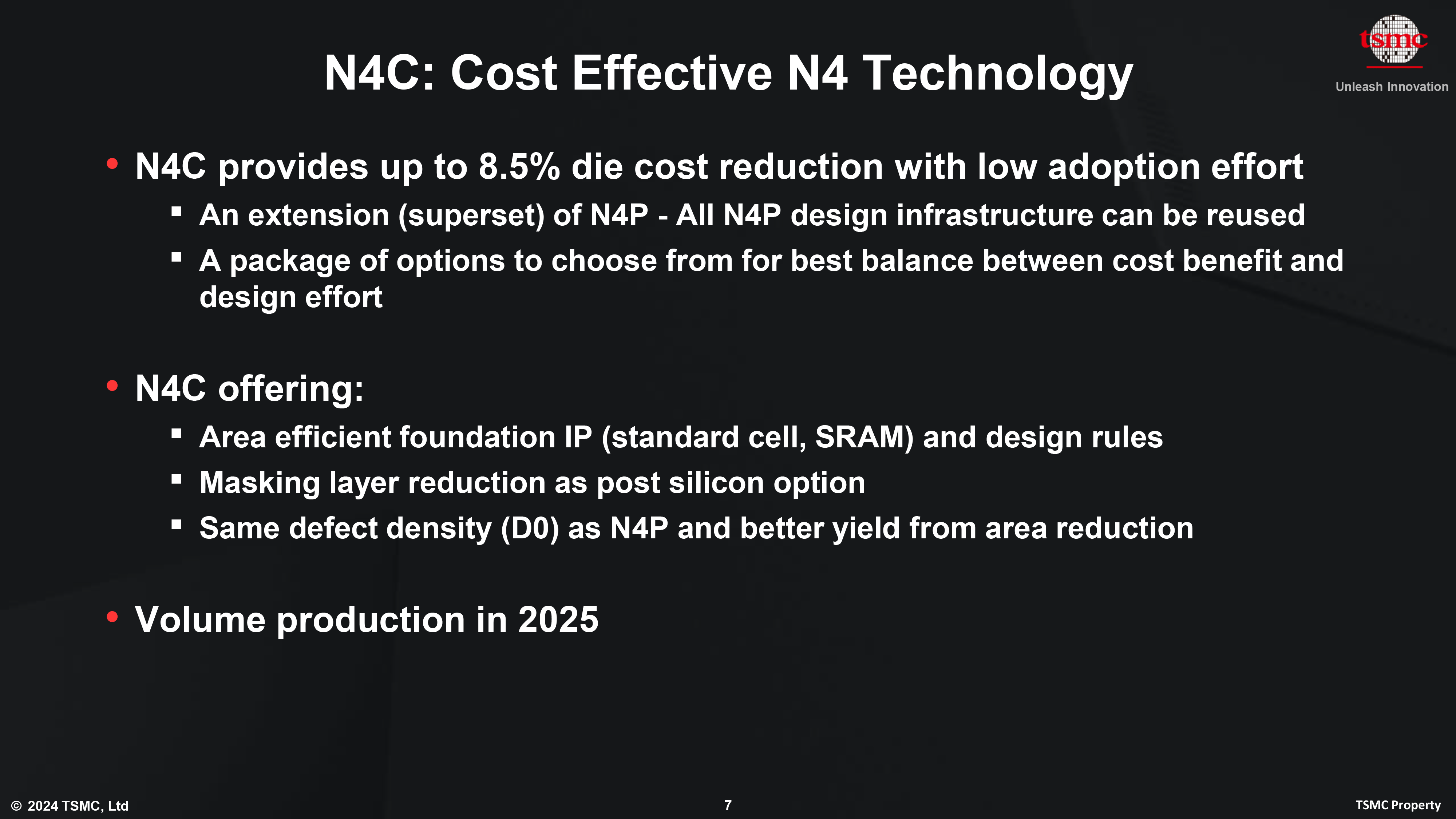
TSMC says that N4C can use the same design infrastructure as N4P, though it is unclear whether N5 and N4P IP can be re-used for N4C-based chips. Meanwhile, TSMC indicates that it offers various options for chipmakers to find the right balance between cost benefits and design effort, so companies interested in adopting a 4nm-class process technologies could well adopt N4C.
The development of N4C comes as many of TSMC's chip design customers are preparing to launch chips based on the company's final generation of FinFET process technology, the 3nm N3 series. While N3 is expected to be a successful family, the high costs of N3B have been an issue, and the generation is marked by diminishing performance and transistor density returns altogether. Consequently, N4C could well become a major, long-lived node at TSMC, serving as a good fit for customers who want to stick to a more cost-effective FinFET node.
"This is a very significant enhancement, we are working with our customer, basically to extract more value from their 4 nm investment," Zhang said.
TSMC expects to start volume production of N4C chips some time next year. And with TSMC having produced 5nm-class for nearly half a decade at that point, N4C should be able to hit the ground running in terms of volume and yields.

Lorem Ipsum is simply dummy text of the printing and typesetting industry. Lorem Ipsum has been the industry's.
Further to our last piece which we detailed Intel's issue to motherboard vendors to follow with stock power settings for Intel's 14th and 13th Gen Core series processors, Intel has now issued a follow-up statement to this. Over the last week or so, motherboard vendors quickly released firmware updates with a new profile called 'Intel Baseline', which motherboard vendors assumed would address the instability issues.
As it turns out, Intel doesn't seem to accept this as technically, these Intel Baseline profiles are not to be confused with Intel's default specifications. This means that Intel's Baseline profiles seemingly give the impression that they are operating at default settings, hence the terminology 'baseline' used, but this still opens motherboard vendors to use their interpretations of MCE or Multi-Core Enhancement.
To clarify things for consumers, Intel has sent us the following statement:
Several motherboard manufacturers have released BIOS profiles labeled ‘Intel Baseline Profile’. However, these BIOS profiles are not the same as the 'Intel Default Settings' recommendations that Intel has recently shared with its partners regarding the instability issues reported on 13th and 14th gen K SKU processors.
These ‘Intel Baseline Profile’ BIOS settings appear to be based on power delivery guidance previously provided by Intel to manufacturers describing the various power delivery options for 13th and 14th Generation K SKU processors based on motherboard capabilities.
Intel is not recommending motherboard manufacturers to use ‘baseline’ power delivery settings on boards capable of higher values.
Intel’s recommended ‘Intel Default Settings’ are a combination of thermal and power delivery features along with a selection of possible power delivery profiles based on motherboard capabilities.
Intel recommends customers to implement the highest power delivery profile compatible with each individual motherboard design as noted in the table below:
Click to Enlarge Intel's Default Settings
What Intel's statement is effectively saying to consumers, is that users shouldn't be using the Baseline Power Delivery profiles which are offered by motherboard vendors through a plethora of firmware updates. Instead, Intel is recommending users opt for Intel Default Settings, which follows what the specific processor is rated for by Intel out of the box to achieve the clock speeds advertised, without users having to worry about firmware 'over' optimization which can cause instability as there have been many reports of happening.
Not only this, but the Intel Default settings offer a combination of thermal specifications and power capabilities, including voltage and frequency curve settings that apply to the capability of the motherboard used, and the power delivery equipped on the motherboard. At least for the most part, Intel is recommending users with 14th and 13th-Gen Core series K, KF, and KS SKUs that they do not recommend users opt in using the Baseline profiles offered by motherboard vendors.
Digesting the contrast between the two statements, the key differential is that Intel's priority is reducing the current going through the processor, which for both the 14th and 13th Gen Core series processors is a maximum of 400 A, even when using the Extreme profile. We know those motherboard vendors on their Z790 and Z690 motherboards opt for an unrestricted power profile, which is essentially 'unlimited' power and current to maximize performance at the cost of power consumption and heat, which does exacerbate problems and can lead to frequent bouts of instability, especially on high-intensity workloads.
Another variable Intel is recommending is that the AC Load Line must match the design target of the processor, with a maximum value of 1.1 mOhm, and that the DC Load Line must be ... CPUs
Thanks to the success of the burgeoning market for AI accelerators, NVIDIA has been on a tear this year. And the only place that’s even more apparent than the company’s rapidly growing revenues is in the company’s stock price and market capitalization. After breaking into the top 5 most valuable companies only earlier this year, NVIDIA has reached the apex of Wall Street, closing out today as the world’s most valuable company.
With a closing price of $135.58 on a day that saw NVIDIA’s stock pop up another 3.5%, NVIDIA has topped both Microsoft and Apple in valuation, reaching a market capitalization of $3.335 trillion. This follows a rapid rise in the company’s stock price, which has increased by 47% in the last month alone – particularly on the back of NVIDIA’s most recent estimates-beating earnings report – as well as a recent 10-for-1 stock split. And looking at the company’s performance over a longer time period, NVIDIA’s stock jumped a staggering 218% over the last year, or a mere 3,474% over the last 5 years.
NVIDIA’s ascension continues a trend over the last several years of tech companies all holding the top spots in the market capitalization rankings. Though this is the first time in quite a while that the traditional tech leaders of Apple and Microsoft have been pushed aside.
| Market Capitalization Rankings | ||
| Market Cap | Stock Price | |
| NVIDIA | $3.335T | $135.58 |
| Microsoft | $3.317T | $446.34 |
| Apple | $3.285T | $214.29 |
| Alphabet | $2.170T | $176.45 |
| Amazon | $1.902T | $182.81 |
Driving the rapid growth of NVIDIA and its market capitalization has been demand for AI accelerators from NVIDIA, particularly the company’s server-grade H100, H200, and GH200 accelerators for AI training. As the demand for these products has spiked, NVIDIA has been scaling up accordingly, repeatedly beating market expectations for how many of the accelerators they can ship – and what price they can charge. And despite all that growth, orders for NVIDIA’s high-end accelerators are still backlogged, underscoring how NVIDIA still isn’t meeting the full demands of hyperscalers and other enterprises.
Consequently, NVIDIA’s stock price and market capitalization have been on a tear on the basis of these future expectations. With a price-to-earnings (P/E) ratio of 76.7 – more than twice that of Microsoft or Apple – NVIDIA is priced more like a start-up than a 30-year-old tech company. But then it goes without saying that most 30-year-old tech companies aren’t tripling their revenue in a single year, placing NVIDIA in a rather unique situation at this time.
Like the stock market itself, market capitalizations are highly volatile. And historically speaking, it’s far from guaranteed that NVIDIA will be able to hold the top spot for long, never mind day-to-day fluctuations. NVIDIA, Apple, and Microsoft’s valuations are all within $50 billion (1.%) of each other, so for the moment at least, it’s still a tight race between all three companies. But no matter what happens from here, NVIDIA gets the exceptionally rare claim of having been the most valuable company in the world at some point.
(Carousel image courtesy MSN Money)
GPUs
Kioxia's booth at FMS 2024 was a busy one with multiple technology demonstrations keeping visitors occupied. A walk-through of the BiCS 8 manufacturing process was the first to grab my attention. Kioxia and Western Digital announced the sampling of BiCS 8 in March 2023. We had touched briefly upon its CMOS Bonded Array (CBA) scheme in our coverage of Kioxial's 2Tb QLC NAND device and coverage of Western Digital's 128 TB QLC enterprise SSD proof-of-concept demonstration. At Kioxia's booth, we got more insights.
Traditionally, fabrication of flash chips involved placement of the associate logic circuitry (CMOS process) around the periphery of the flash array. The process then moved on to putting the CMOS under the cell array, but the wafer development process was serialized with the CMOS logic getting fabricated first followed by the cell array on top. However, this has some challenges because the cell array requires a high-temperature processing step to ensure higher reliability that can be detrimental to the health of the CMOS logic. Thanks to recent advancements in wafer bonding techniques, the new CBA process allows the CMOS wafer and cell array wafer to be processed independently in parallel and then pieced together, as shown in the models above.
The BiCS 8 3D NAND incorporates 218 layers, compared to 112 layers in BiCS 5 and 162 layers in BiCS 6. The company decided to skip over BiCS 7 (or, rather, it was probably a short-lived generation meant as an internal test vehicle). The generation retains the four-plane charge trap structure of BiCS 6. In its TLC avatar, it is available as a 1 Tbit device. The QLC version is available in two capacities - 1 Tbit and 2 Tbit.
Kioxia also noted that while the number of layers (218) doesn't compare favorably with the latest layer counts from the competition, its lateral scaling / cell shrinkage has enabled it to be competitive in terms of bit density as well as operating speeds (3200 MT/s). For reference, the latest shipping NAND from Micron - the G9 - has 276 layers with a bit density in TLC mode of 21 Gbit/mm2, and operates at up to 3600 MT/s. However, its 232L NAND operates only up to 2400 MT/s and has a bit density of 14.6 Gbit/mm2.
It must be noted that the CBA hybrid bonding process has advantages over the current processes used by other vendors - including Micron's CMOS under array (CuA) and SK hynix's 4D PUC (periphery-under-chip) developed in the late 2010s. It is expected that other NAND vendors will also move eventually to some variant of the hybrid bonding scheme used by Kioxia.
Storage


 allocated <a href="https://green-innovation.nedo.go.jp/en/project/building-next-generation-digital-infrastructure/summary/">funding</a> for the development of green datacenter technologies. With the aim to obtain up to 40% savings in overall power consumption, several Japanese companies have been developing an optical interface for their enterprise SSDs. And at this year's FMS, Kioxia had their optical interface on display.</p>
<p align="center"><a href="https://www.anandtech.com/show/21520/kioxia-demonstrates-optical-interface-ssds-for-data-centers"><img alt="" src="https://images.anandtech.com/doci/21520/opt-ssd0_575px.jpg" /></a></p>
<p>For this demonstration, Kioxia took its existing CM7 enterprise SSD and created an optical interface for it. A PCIe card with on-board optics developed by Kyocera is installed in the server slot. An optical interface allows data transfer over long distances (it was 40m in the demo, but Kioxia promises lengths of up to 100m for the cable in the future). This allows the storage to be kept in a separate room with minimal cooling requirements compared to the rack with the CPUs and GPUs. Disaggregation of different server components will become an option as very high throughput interfaces such as PCIe 7.0 (with 128 GT/s rates) become available.</p>
<p align="center"><a href="https://www.anandtech.com/show/21520/kioxia-demonstrates-optical-interface-ssds-for-data-centers"><img alt="" src="https://images.anandtech.com/doci/21520/opt-ssd1_575px.jpg" /></a></p>
<p>The demonstration of the optical SSD showed a slight loss in IOPS performance, but a significant advantage in the latency metric over the shipping enterprise SSD behind a copper network link. Obviously, there are advantages in wiring requirements and signal integrity maintenance with optical links.</p>
<p>Being a proof-of-concept demonstration, we do see the requirement for an industry-standard approach if this were to gain adoption among different datacenter vendors. The <a href="https://www.anandtech.com/show/19990/pcisig-forms-optical-workgroup-lighting-the-way-to-pcies-future">PCI-SIG optical workgroup</a> will need to get its act together soon to create a standards-based approach to this problem.</p>
</p> Storage)
 allocated <a href="https://green-innovation.nedo.go.jp/en/project/building-next-generation-digital-infrastructure/summary/">funding</a> for the development of green datacenter technologies. With the aim to obtain up to 40% savings in overall power consumption, several Japanese companies have been developing an optical interface for their enterprise SSDs. And at this year's FMS, Kioxia had their optical interface on display.</p>
<p align="center"><a href="https://www.anandtech.com/show/21520/kioxia-demonstrates-optical-interface-ssds-for-data-centers"><img alt="" src="https://images.anandtech.com/doci/21520/opt-ssd0_575px.jpg" /></a></p>
<p>For this demonstration, Kioxia took its existing CM7 enterprise SSD and created an optical interface for it. A PCIe card with on-board optics developed by Kyocera is installed in the server slot. An optical interface allows data transfer over long distances (it was 40m in the demo, but Kioxia promises lengths of up to 100m for the cable in the future). This allows the storage to be kept in a separate room with minimal cooling requirements compared to the rack with the CPUs and GPUs. Disaggregation of different server components will become an option as very high throughput interfaces such as PCIe 7.0 (with 128 GT/s rates) become available.</p>
<p align="center"><a href="https://www.anandtech.com/show/21520/kioxia-demonstrates-optical-interface-ssds-for-data-centers"><img alt="" src="https://images.anandtech.com/doci/21520/opt-ssd1_575px.jpg" /></a></p>
<p>The demonstration of the optical SSD showed a slight loss in IOPS performance, but a significant advantage in the latency metric over the shipping enterprise SSD behind a copper network link. Obviously, there are advantages in wiring requirements and signal integrity maintenance with optical links.</p>
<p>Being a proof-of-concept demonstration, we do see the requirement for an industry-standard approach if this were to gain adoption among different datacenter vendors. The <a href="https://www.anandtech.com/show/19990/pcisig-forms-optical-workgroup-lighting-the-way-to-pcies-future">PCI-SIG optical workgroup</a> will need to get its act together soon to create a standards-based approach to this problem.</p>
</p> Storage | https://compbuddey.blogspot.com/2024/09/kioxia-demonstrates-optical-interface_54.html)
 allocated <a href="https://green-innovation.nedo.go.jp/en/project/building-next-generation-digital-infrastructure/summary/">funding</a> for the development of green datacenter technologies. With the aim to obtain up to 40% savings in overall power consumption, several Japanese companies have been developing an optical interface for their enterprise SSDs. And at this year's FMS, Kioxia had their optical interface on display.</p>
<p align="center"><a href="https://www.anandtech.com/show/21520/kioxia-demonstrates-optical-interface-ssds-for-data-centers"><img alt="" src="https://images.anandtech.com/doci/21520/opt-ssd0_575px.jpg" /></a></p>
<p>For this demonstration, Kioxia took its existing CM7 enterprise SSD and created an optical interface for it. A PCIe card with on-board optics developed by Kyocera is installed in the server slot. An optical interface allows data transfer over long distances (it was 40m in the demo, but Kioxia promises lengths of up to 100m for the cable in the future). This allows the storage to be kept in a separate room with minimal cooling requirements compared to the rack with the CPUs and GPUs. Disaggregation of different server components will become an option as very high throughput interfaces such as PCIe 7.0 (with 128 GT/s rates) become available.</p>
<p align="center"><a href="https://www.anandtech.com/show/21520/kioxia-demonstrates-optical-interface-ssds-for-data-centers"><img alt="" src="https://images.anandtech.com/doci/21520/opt-ssd1_575px.jpg" /></a></p>
<p>The demonstration of the optical SSD showed a slight loss in IOPS performance, but a significant advantage in the latency metric over the shipping enterprise SSD behind a copper network link. Obviously, there are advantages in wiring requirements and signal integrity maintenance with optical links.</p>
<p>Being a proof-of-concept demonstration, we do see the requirement for an industry-standard approach if this were to gain adoption among different datacenter vendors. The <a href="https://www.anandtech.com/show/19990/pcisig-forms-optical-workgroup-lighting-the-way-to-pcies-future">PCI-SIG optical workgroup</a> will need to get its act together soon to create a standards-based approach to this problem.</p>
</p> Storage&body=https://compbuddey.blogspot.com/2024/09/kioxia-demonstrates-optical-interface_54.html)
0 Comments