
Following Intel’s painful Q2 earnings call and the announcement of their 2025 cost reduction plan last week, it has become increasingly evident that Intel’s future is in the hands of their foundry group. Between Intel’s IDM 2.0 initiative and their internal chip production plans, all roads lead back to Intel retaking – and retaining – fab process leadership. To win as both a chip designer and a contract chip maker, Intel needs to be able to regain the fab technology lead it once held. In many respects it’s a return to Intel’s classic (and most successful) operating model, but never has it been so risky at it is for the already weakened Intel.
Intel’s do-or-die dash for process leadership means that, for the next 18 months or so, all eyes are on the company’s 20A and 18A process nodes. The final nodes in their ambitious 5 Nodes in 4 Years roadmap, the twinned 20A/18A are the culmination of several new technologies, primarily Intel’s GAAFET implementation (RibbonFET), which is being combined with PowerVia, Intel’s backside power delivery network (BS-PDN) technology. 20A is set to serve as Intel’s early version of the node, and 18A the refined version for long-term use both internally, and as the first major external node for Intel Foundry. To say that everything rides on Intel 18A isn’t quite accurate, but it’s only a slight embellishment.
To that end, we’re going to see Intel deliver a lot of status updates on 18A over the next year as they continue to outline to investors and external customers alike that they have the manufacturing side of their business in order. And today is one of those days, with a fresh update on the state of 18A.
So what’s new with 18A? The biggest news out of Intel this morning is that their first 18A chips are back from the development fab and are successfully booting operating systems. This means the silicon not only works (power-on), but works well enough to complete core tasks. It’s a major step in bringing up a chip, and at this point, Intel wants to make sure to let the whole world know.
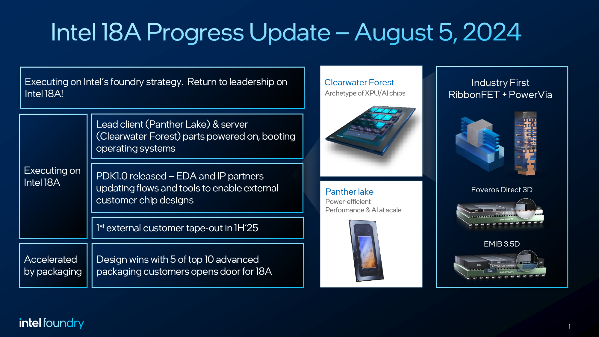
Earlier this year the company finished taping out both of its lead 18A chips: Panther Lake for clients, and Clearwater Forest for servers. And it’s both chips that are booting. This is made all the more significant by the fact that Clearwater Forest also relies on Intel’s die-to-die hybrid bonding packaging technology, Foveros Direct 3D, where it will be the lead product for that technology as well. Which for Intel, is a promising sign that not only are their silicon lithography ambitions paying off, but their intention to lead in advanced packaging is on-track as well.
And while Intel doesn’t normally talk about yields this early in the game, it’s interesting to note that in a separate Q&A being published this morning with Intel Foundry’s new boss, Kevin O’Buckley, the head of Foundry Services explicitly comments that Panther Lake is “yielding well”. Similarly, Panther Lake’s DDR memory controller (a complex block mixing logic with a PHY) is already running at its target frequency. Progress is going so well, apparently, that according to O’Buckley, it’s ahead of schedule on its product qualification milestones.
As for Intel’s contract foundry business, the company is ramping up its efforts there now that the first full process design kit (PDK) is ready for 18A. Intel released their 18A PDK 1.0 last month, giving Intel’s customers (and potential customers) the tools to finally finish designing their chips for production. As is typically the case of a new node, pre-release PDKs were available for companies to get start... CPUs


Samsung had quietly launched its BM1743 enterprise QLC SSD last month with a hefty 61.44 TB SKU. At FMS 2024, the company had the even larger 122.88 TB version of that SSD on display, alongside a few recorded benchmarking sessions. Compared to the previous generation, the BM1743 comes with a 4.1x improvement in I/O performance, improvement in data retention, and a 45% improvement in power efficiency for sequential writes.

The 128 TB-class QLC SSD boasts of sequential read speeds of 7.5 GBps and write speeds of 3 GBps. Random reads come in at 1.6 M IOPS, while 16 KB random writes clock in at 45K IOPS. Based on the quoted random write access granularity, it appears that Samsung is using a 16 KB indirection unit (IU) to optimize flash management. This is similar to the strategy adopted by Solidigm with IUs larger than 4K in their high-capacity SSDs.
A recorded benchmark session on the company's PM9D3a 8-channel Gen 5 SSD was also on display.

The SSD family is being promoted as a mainstream option for datacenters, and boasts of sequential reads up to 12 GBps and writes up to 6.8 GBps. Random reads clock in at 2 M IOPS, and random writes at 400 K IOPS.

Available in multiple form-factors up to 32 TB (M.2 tops out at 2 TB), the drive's firmware includes optional support for flexible data placement (FDP) to help address the write amplification aspect.
The PM1753 is the current enterprise SSD flagship in Samsung's lineup. With support for 16 NAND channels and capacities up to 32 TB, this U.2 / E3.S SSD has advertised sequential read and write speeds of 14.8 GBps and 11 GBps respectively. Random reads and writes for 4 KB accesses are listed at 3.4 M and 600 K IOPS.

Samsung claims a 1.7x performance improvement and a 1.7x power efficiency improvement over the previous generation (PM1743), making this TLC SSD suitable for AI servers.
The 9th Gen. V-NAND wafer was also available for viewing, though photography was prohibited. Mass production of this flash memory began in April 2024.
Storage
As the second quarter of 2024 is soon set to unfold, there are many things to be excited about, especially as Computex 2024 has been and gone. We now know that AMD's upcoming Ryzen 9000 series desktop processors using the new Zen 5 cores will be hitting shelves at the end of the month (31st July), and on top of this, AMD also recently slashed pricing on their Zen 4 (Ryzen 8000) processors. Intel still needs to follow suit with their 14th or 13th Gen Core series processors, but right now from a cost standpoint, AMD is in a much better position.
Since the publication of our last guide, the only notable CPU to be launched was Intel's special binned Core i9-14900KS, which not only pushes clock speeds up to 6.2 GHz but is the last processor to feature Intel's iconic Core I series nomenclature. The other big news in the CPU world was from Intel, with a statement issued about pushing users to use the Intel Default Specification on Intel's 14th and 13th Gen processors, which ultimately limits the performance compared to published data. We're still in the process of
While the CPU market has been relatively quiet so far this year, and things are set to pick up once AMD's Zen 5 and Intel's Arrow Lake desktop chips are all launched onto the market, it means today we are working for the same hymn sheet as our previous guide. With AMD's price drops on Ryzen 7000 series processors, much of the guide reflects this as AMD and Intel's performance is neck and neck in many use cases, but cost certainly plays a big factor in selecting a new CPU. As we move into the rest of 2024, the CPU market looks set to see the rise of the 'AI PC,' which is looking set to be something that many companies will focus on by the end of 2024, both on mobile and desktop platforms.
Guides
Samsung had quietly launched its BM1743 enterprise QLC SSD last month with a hefty 61.44 TB SKU. At FMS 2024, the company had the even larger 122.88 TB version of that SSD on display, alongside a few recorded benchmarking sessions. Compared to the previous generation, the BM1743 comes with a 4.1x improvement in I/O performance, improvement in data retention, and a 45% improvement in power efficiency for sequential writes.
The 128 TB-class QLC SSD boasts of sequential read speeds of 7.5 GBps and write speeds of 3 GBps. Random reads come in at 1.6 M IOPS, while 16 KB random writes clock in at 45K IOPS. Based on the quoted random write access granularity, it appears that Samsung is using a 16 KB indirection unit (IU) to optimize flash management. This is similar to the strategy adopted by Solidigm with IUs larger than 4K in their high-capacity SSDs.
A recorded benchmark session on the company's PM9D3a 8-channel Gen 5 SSD was also on display.
The SSD family is being promoted as a mainstream option for datacenters, and boasts of sequential reads up to 12 GBps and writes up to 6.8 GBps. Random reads clock in at 2 M IOPS, and random writes at 400 K IOPS.
Available in multiple form-factors up to 32 TB (M.2 tops out at 2 TB), the drive's firmware includes optional support for flexible data placement (FDP) to help address the write amplification aspect.
The PM1753 is the current enterprise SSD flagship in Samsung's lineup. With support for 16 NAND channels and capacities up to 32 TB, this U.2 / E3.S SSD has advertised sequential read and write speeds of 14.8 GBps and 11 GBps respectively. Random reads and writes for 4 KB accesses are listed at 3.4 M and 600 K IOPS.
Samsung claims a 1.7x performance improvement and a 1.7x power efficiency improvement over the previous generation (PM1743), making this TLC SSD suitable for AI servers.
The 9th Gen. V-NAND wafer was also available for viewing, though photography was prohibited. Mass production of this flash memory began in April 2024.
Storage
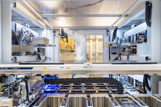
At FMS 2024, the technological requirements from the storage and memory subsystem took center stage. Both SSD and controller vendors had various demonstrations touting their suitability for different stages of the AI data pipeline - ingestion, preparation, training, checkpointing, and inference. Vendors like Solidigm have different types of SSDs optimized for different stages of the pipeline. At the same time, controller vendors have taken advantage of one of the features introduced recently in the NVM Express standard - Flexible Data Placement (FDP).
FDP involves the host providing information / hints about the areas where the controller could place the incoming write data in order to reduce the write amplification. These hints are generated based on specific block sizes advertised by the device. The feature is completely backwards-compatible, with non-FDP hosts working just as before with FDP-enabled SSDs, and vice-versa.
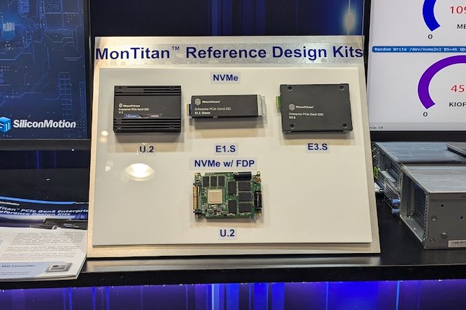
Silicon Motion's MonTitan Gen 5 Enterprise SSD Platform was announced back in 2022. Since then, Silicon Motion has been touting the flexibility of the platform, allowing its customers to incorporate their own features as part of the customization process. This approach is common in the enterprise space, as we have seen with Marvell's Bravera SC5 SSD controller in the DapuStor SSDs and Microchip's Flashtec controllers in the Longsys FORESEE enterprise SSDs.
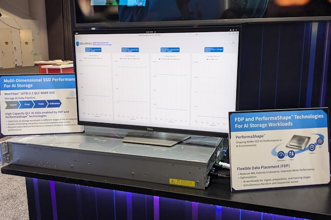
At FMS 2024, the company was demonstrating the advantages of flexible data placement by allowing a single QLC SSD based on their MonTitan platform to take part in different stages of the AI data pipeline while maintaining the required quality of service (minimum bandwidth) for each process. The company even has a trademarked name (PerformaShape) for the firmware feature in the controller that allows the isolation of different concurrent SSD accesses (from different stages in the AI data pipeline) to guarantee this QoS. Silicon Motion claims that this scheme will enable its customers to get the maximum write performance possible from QLC SSDs without negatively impacting the performance of other types of accesses.
Silicon Motion and Phison have market leadership in the client SSD controller market with similar approaches. However, their enterprise SSD controller marketing couldn't be more different. While Phison has gone in for a turnkey solution with their Gen 5 SSD platform (to the extent of not adopting the white label route for this generation, and instead opting to get the SSDs qualified with different cloud service providers themselves), Silicon Motion is opting for a different approach. The flexibility and customization possibilities can make platforms like the MonTitan appeal to flash array vendors.
Storage
Samsung had quietly launched its BM1743 enterprise QLC SSD last month with a hefty 61.44 TB SKU. At FMS 2024, the company had the even larger 122.88 TB version of that SSD on display, alongside a few recorded benchmarking sessions. Compared to the previous generation, the BM1743 comes with a 4.1x improvement in I/O performance, improvement in data retention, and a 45% improvement in power efficiency for sequential writes.
The 128 TB-class QLC SSD boasts of sequential read speeds of 7.5 GBps and write speeds of 3 GBps. Random reads come in at 1.6 M IOPS, while 16 KB random writes clock in at 45K IOPS. Based on the quoted random write access granularity, it appears that Samsung is using a 16 KB indirection unit (IU) to optimize flash management. This is similar to the strategy adopted by Solidigm with IUs larger than 4K in their high-capacity SSDs.
A recorded benchmark session on the company's PM9D3a 8-channel Gen 5 SSD was also on display.
The SSD family is being promoted as a mainstream option for datacenters, and boasts of sequential reads up to 12 GBps and writes up to 6.8 GBps. Random reads clock in at 2 M IOPS, and random writes at 400 K IOPS.
Available in multiple form-factors up to 32 TB (M.2 tops out at 2 TB), the drive's firmware includes optional support for flexible data placement (FDP) to help address the write amplification aspect.
The PM1753 is the current enterprise SSD flagship in Samsung's lineup. With support for 16 NAND channels and capacities up to 32 TB, this U.2 / E3.S SSD has advertised sequential read and write speeds of 14.8 GBps and 11 GBps respectively. Random reads and writes for 4 KB accesses are listed at 3.4 M and 600 K IOPS.
Samsung claims a 1.7x performance improvement and a 1.7x power efficiency improvement over the previous generation (PM1743), making this TLC SSD suitable for AI servers.
The 9th Gen. V-NAND wafer was also available for viewing, though photography was prohibited. Mass production of this flash memory began in April 2024.
Storage
As the second quarter of 2024 is soon set to unfold, there are many things to be excited about, especially as Computex 2024 has been and gone. We now know that AMD's upcoming Ryzen 9000 series desktop processors using the new Zen 5 cores will be hitting shelves at the end of the month (31st July), and on top of this, AMD also recently slashed pricing on their Zen 4 (Ryzen 8000) processors. Intel still needs to follow suit with their 14th or 13th Gen Core series processors, but right now from a cost standpoint, AMD is in a much better position.
Since the publication of our last guide, the only notable CPU to be launched was Intel's special binned Core i9-14900KS, which not only pushes clock speeds up to 6.2 GHz but is the last processor to feature Intel's iconic Core I series nomenclature. The other big news in the CPU world was from Intel, with a statement issued about pushing users to use the Intel Default Specification on Intel's 14th and 13th Gen processors, which ultimately limits the performance compared to published data. We're still in the process of
While the CPU market has been relatively quiet so far this year, and things are set to pick up once AMD's Zen 5 and Intel's Arrow Lake desktop chips are all launched onto the market, it means today we are working for the same hymn sheet as our previous guide. With AMD's price drops on Ryzen 7000 series processors, much of the guide reflects this as AMD and Intel's performance is neck and neck in many use cases, but cost certainly plays a big factor in selecting a new CPU. As we move into the rest of 2024, the CPU market looks set to see the rise of the 'AI PC,' which is looking set to be something that many companies will focus on by the end of 2024, both on mobile and desktop platforms.
Guides
Samsung had quietly launched its BM1743 enterprise QLC SSD last month with a hefty 61.44 TB SKU. At FMS 2024, the company had the even larger 122.88 TB version of that SSD on display, alongside a few recorded benchmarking sessions. Compared to the previous generation, the BM1743 comes with a 4.1x improvement in I/O performance, improvement in data retention, and a 45% improvement in power efficiency for sequential writes.
The 128 TB-class QLC SSD boasts of sequential read speeds of 7.5 GBps and write speeds of 3 GBps. Random reads come in at 1.6 M IOPS, while 16 KB random writes clock in at 45K IOPS. Based on the quoted random write access granularity, it appears that Samsung is using a 16 KB indirection unit (IU) to optimize flash management. This is similar to the strategy adopted by Solidigm with IUs larger than 4K in their high-capacity SSDs.
A recorded benchmark session on the company's PM9D3a 8-channel Gen 5 SSD was also on display.
The SSD family is being promoted as a mainstream option for datacenters, and boasts of sequential reads up to 12 GBps and writes up to 6.8 GBps. Random reads clock in at 2 M IOPS, and random writes at 400 K IOPS.
Available in multiple form-factors up to 32 TB (M.2 tops out at 2 TB), the drive's firmware includes optional support for flexible data placement (FDP) to help address the write amplification aspect.
The PM1753 is the current enterprise SSD flagship in Samsung's lineup. With support for 16 NAND channels and capacities up to 32 TB, this U.2 / E3.S SSD has advertised sequential read and write speeds of 14.8 GBps and 11 GBps respectively. Random reads and writes for 4 KB accesses are listed at 3.4 M and 600 K IOPS.
Samsung claims a 1.7x performance improvement and a 1.7x power efficiency improvement over the previous generation (PM1743), making this TLC SSD suitable for AI servers.
The 9th Gen. V-NAND wafer was also available for viewing, though photography was prohibited. Mass production of this flash memory began in April 2024.
Storage
At FMS 2024, the technological requirements from the storage and memory subsystem took center stage. Both SSD and controller vendors had various demonstrations touting their suitability for different stages of the AI data pipeline - ingestion, preparation, training, checkpointing, and inference. Vendors like Solidigm have different types of SSDs optimized for different stages of the pipeline. At the same time, controller vendors have taken advantage of one of the features introduced recently in the NVM Express standard - Flexible Data Placement (FDP).
FDP involves the host providing information / hints about the areas where the controller could place the incoming write data in order to reduce the write amplification. These hints are generated based on specific block sizes advertised by the device. The feature is completely backwards-compatible, with non-FDP hosts working just as before with FDP-enabled SSDs, and vice-versa.
Silicon Motion's MonTitan Gen 5 Enterprise SSD Platform was announced back in 2022. Since then, Silicon Motion has been touting the flexibility of the platform, allowing its customers to incorporate their own features as part of the customization process. This approach is common in the enterprise space, as we have seen with Marvell's Bravera SC5 SSD controller in the DapuStor SSDs and Microchip's Flashtec controllers in the Longsys FORESEE enterprise SSDs.
At FMS 2024, the company was demonstrating the advantages of flexible data placement by allowing a single QLC SSD based on their MonTitan platform to take part in different stages of the AI data pipeline while maintaining the required quality of service (minimum bandwidth) for each process. The company even has a trademarked name (PerformaShape) for the firmware feature in the controller that allows the isolation of different concurrent SSD accesses (from different stages in the AI data pipeline) to guarantee this QoS. Silicon Motion claims that this scheme will enable its customers to get the maximum write performance possible from QLC SSDs without negatively impacting the performance of other types of accesses.
Silicon Motion and Phison have market leadership in the client SSD controller market with similar approaches. However, their enterprise SSD controller marketing couldn't be more different. While Phison has gone in for a turnkey solution with their Gen 5 SSD platform (to the extent of not adopting the white label route for this generation, and instead opting to get the SSDs qualified with different cloud service providers themselves), Silicon Motion is opting for a different approach. The flexibility and customization possibilities can make platforms like the MonTitan appeal to flash array vendors.
Storage

Kioxia's booth at FMS 2024 was a busy one with multiple technology demonstrations keeping visitors occupied. A walk-through of the BiCS 8 manufacturing process was the first to grab my attention. Kioxia and Western Digital announced the sampling of BiCS 8 in March 2023. We had touched briefly upon its CMOS Bonded Array (CBA) scheme in our coverage of Kioxial's 2Tb QLC NAND device and coverage of Western Digital's 128 TB QLC enterprise SSD proof-of-concept demonstration. At Kioxia's booth, we got more insights.

Traditionally, fabrication of flash chips involved placement of the associate logic circuitry (CMOS process) around the periphery of the flash array. The process then moved on to putting the CMOS under the cell array, but the wafer development process was serialized with the CMOS logic getting fabricated first followed by the cell array on top. However, this has some challenges because the cell array requires a high-temperature processing step to ensure higher reliability that can be detrimental to the health of the CMOS logic. Thanks to recent advancements in wafer bonding techniques, the new CBA process allows the CMOS wafer and cell array wafer to be processed independently in parallel and then pieced together, as shown in the models above.

The BiCS 8 3D NAND incorporates 218 layers, compared to 112 layers in BiCS 5 and 162 layers in BiCS 6. The company decided to skip over BiCS 7 (or, rather, it was probably a short-lived generation meant as an internal test vehicle). The generation retains the four-plane charge trap structure of BiCS 6. In its TLC avatar, it is available as a 1 Tbit device. The QLC version is available in two capacities - 1 Tbit and 2 Tbit.
Kioxia also noted that while the number of layers (218) doesn't compare favorably with the latest layer counts from the competition, its lateral scaling / cell shrinkage has enabled it to be competitive in terms of bit density as well as operating speeds (3200 MT/s). For reference, the latest shipping NAND from Micron - the G9 - has 276 layers with a bit density in TLC mode of 21 Gbit/mm2, and operates at up to 3600 MT/s. However, its 232L NAND operates only up to 2400 MT/s and has a bit density of 14.6 Gbit/mm2.
It must be noted that the CBA hybrid bonding process has advantages over the current processes used by other vendors - including Micron's CMOS under array (CuA) and SK hynix's 4D PUC (periphery-under-chip) developed in the late 2010s. It is expected that other NAND vendors will also move eventually to some variant of the hybrid bonding scheme used by Kioxia.
Storage![Rapidus Adds Chip Packaging Services to Plans for $32 Billion 2nm Fab <p align="center"><a href="https://www.anandtech.com/show/21411/rapidus-adds-chip-packaging-services-to-plans-for-32b-2nm-fab"><img src="https://images.anandtech.com/doci/21411/microsoft-azure-datacenter-custom-chip-processor-wafer-semiconductor-fab-678_575px.jpg" alt="" /></a></p><p><p>To say that the global foundry market is booming right now would be an understatement. Demand for leading-edge process technologies driven by AI and HPC applications is unprecedented, and with Intel joining the contract chipmaking game, this market segment is once again becoming rather competitive as well. Yet, this is exactly the market segment that Rapidus, a foundry startup backed by the Japanese government and several major Japanese companies, is going to enter in 2027, when its first fab comes online, just a few years from now.</p>
<p>In a fresh update on the status of bringing up the company's first leading-edge fab, Rapidus has revealed that they are intending to get in to the chip packaging game as well. Once complete, the ¥5 trillion ($32 billion) fab will be offering both chip lithography on a 2nm node, as well as packaging services for chips produced within the facility – a notable distinction in an industry where, even if packaging isn't outsourced entirely (OSAT), it's still normally handled at dedicated facilities.</p>
<p>Ultimately, while the company wants to serve the same clients as TSMC, Samsung, and Intel Foundry, the firm plans to do things almost completely differently than its competitors in a bid to speed up chipmaking from finishing design to getting a working chip out of the fab.</p>
<p>"We are very proud of being Japanese," said Henri Richard, general manager and president of Rapidus's subsidiary in the U.S. "[…] I know that some people may be looking at this thinking [that] Japan is known for quality, attention to detail, but not necessarily for speed, or flexibility. But I will tell you that Atsuyoshi Koike (the head of Rapidus) is a very special executive. That is, he has all the quality of Japan, with a lot of American thinking. So he is quite a unique guy, and certainly extraordinarily focused on creating a company that will be extremely flexible and extremely quick on its feet."</p>
<h3>2nm Only, At First</h3>
<p>Perhaps the most significant difference between Rapidus and traditional foundries is that the company will offer only leading-edge manufacturing technologies to its clients: 2 nm in 2027 (phase 1) and then 1.4 nm in the future (phase 2). This is a stark contrast with other contract fabs, including Intel, which tend to offer their customers a full range of fabrication processes to land more clients and produce more chips. Apparently, Rapidus hopes that that there will be enough Japanese and American chip developers that are inclined to use its 2 nm fabrication process to produce their designs. With that said, the number of chip designers that are using the most advanced production node at any given time is relatively small – limited to large firms who need first-mover advantage and have the margins to justify taking the risk – so it remains to be seen whether Rapidus's business model becomes successful. The company believes it will, since the market of chips made on advanced nodes is growing rapidly.</p>
<p>"Until recently IDC was giving a an estimation of the 2nm and below market as about $80 billion and I think we are going to see soon a revision of the potential to $150 billion," said Richard. "[…] TSMC is the 800 pound gorilla in the space. Samsung is there and Intel is going to enter that space. But the market growth is so significant and the demand is so high, that it does not take a lot of market share for Rapidus to be successful. One of the things that gives me great comfort is that when I talk to our EDA partners, when I talk to our potential clients, it is obvious that the entire industry is looking for alternative supply from a fully independent foundry. There is a place for Samsung in this industry, there is a place for Intel in this industry, the industry is currently owned by TSMC. But another totally independent foundry is more than welcome by all of the ecosystem partners and by the customers. So, I feel really, really good about Rapidus's positioning."</p>
<p>Speaking of advanced process technologies, it is notable that Rapidus does not plan to use ASML's High-NA Twinscan EXE lithography scanners for 2 nm production. Instead, Rapidus is sticking to ASML's proven Low-NA scanners, which will reduce costs of Rapidus's fab, though it will entail usage of EUV double patterning, which brings up costs and lengthens the production cycle in other ways. Even with those trade-offs, <a href="https://www.semianalysis.com/p/asml-dilemma-high-na-euv-is-worse">SemiAnalysis analysts believe</a> that given the cost of High-NA EUV litho tools and halved imaging field, ... Semiconductors](https://lh3.googleusercontent.com/blogger_img_proxy/AEn0k_sdP8uroRT3SPdIsbLXJSAOo_2-D65gql5XTa6SH3LK2JbCIj1EN_18pVrwOAlHRZ0Oa73tPEXdmBZ1KFR6DacMHZyYZ6djWFSSnv_4NmN8YiIaA4vb0JwZ4nyBXKsCMofVIhcNx7oj4F3PK82w7neEBtmwmuV9voZAzJhsdF2nEy2dg0UlAfqGpMzymFyrn6eaW6zY9B7id8Un5-d26WZK6w=w72-h72-p-k-no-nu)
To say that the global foundry market is booming right now would be an understatement. Demand for leading-edge process technologies driven by AI and HPC applications is unprecedented, and with Intel joining the contract chipmaking game, this market segment is once again becoming rather competitive as well. Yet, this is exactly the market segment that Rapidus, a foundry startup backed by the Japanese government and several major Japanese companies, is going to enter in 2027, when its first fab comes online, just a few years from now.
In a fresh update on the status of bringing up the company's first leading-edge fab, Rapidus has revealed that they are intending to get in to the chip packaging game as well. Once complete, the ¥5 trillion ($32 billion) fab will be offering both chip lithography on a 2nm node, as well as packaging services for chips produced within the facility – a notable distinction in an industry where, even if packaging isn't outsourced entirely (OSAT), it's still normally handled at dedicated facilities.
Ultimately, while the company wants to serve the same clients as TSMC, Samsung, and Intel Foundry, the firm plans to do things almost completely differently than its competitors in a bid to speed up chipmaking from finishing design to getting a working chip out of the fab.
"We are very proud of being Japanese," said Henri Richard, general manager and president of Rapidus's subsidiary in the U.S. "[…] I know that some people may be looking at this thinking [that] Japan is known for quality, attention to detail, but not necessarily for speed, or flexibility. But I will tell you that Atsuyoshi Koike (the head of Rapidus) is a very special executive. That is, he has all the quality of Japan, with a lot of American thinking. So he is quite a unique guy, and certainly extraordinarily focused on creating a company that will be extremely flexible and extremely quick on its feet."
Perhaps the most significant difference between Rapidus and traditional foundries is that the company will offer only leading-edge manufacturing technologies to its clients: 2 nm in 2027 (phase 1) and then 1.4 nm in the future (phase 2). This is a stark contrast with other contract fabs, including Intel, which tend to offer their customers a full range of fabrication processes to land more clients and produce more chips. Apparently, Rapidus hopes that that there will be enough Japanese and American chip developers that are inclined to use its 2 nm fabrication process to produce their designs. With that said, the number of chip designers that are using the most advanced production node at any given time is relatively small – limited to large firms who need first-mover advantage and have the margins to justify taking the risk – so it remains to be seen whether Rapidus's business model becomes successful. The company believes it will, since the market of chips made on advanced nodes is growing rapidly.
"Until recently IDC was giving a an estimation of the 2nm and below market as about $80 billion and I think we are going to see soon a revision of the potential to $150 billion," said Richard. "[…] TSMC is the 800 pound gorilla in the space. Samsung is there and Intel is going to enter that space. But the market growth is so significant and the demand is so high, that it does not take a lot of market share for Rapidus to be successful. One of the things that gives me great comfort is that when I talk to our EDA partners, when I talk to our potential clients, it is obvious that the entire industry is looking for alternative supply from a fully independent foundry. There is a place for Samsung in this industry, there is a place for Intel in this industry, the industry is currently owned by TSMC. But another totally independent foundry is more than welcome by all of the ecosystem partners and by the customers. So, I feel really, really good about Rapidus's positioning."
Speaking of advanced process technologies, it is notable that Rapidus does not plan to use ASML's High-NA Twinscan EXE lithography scanners for 2 nm production. Instead, Rapidus is sticking to ASML's proven Low-NA scanners, which will reduce costs of Rapidus's fab, though it will entail usage of EUV double patterning, which brings up costs and lengthens the production cycle in other ways. Even with those trade-offs, SemiAnalysis analysts believe that given the cost of High-NA EUV litho tools and halved imaging field, ... Semiconductors

The CXL consortium has had a regular presence at FMS (which rechristened itself from 'Flash Memory Summit' to the 'Future of Memory and Storage' this year). Back at FMS 2022, the company had announced v3.0 of the CXL specifications. This was followed by CXL 3.1's introduction at Supercomputing 2023. Having started off as a host to device interconnect standard, it had slowly subsumed other competing standards such as OpenCAPI and Gen-Z. As a result, the specifications started to encompass a wide variety of use-cases by building a protocol on top of the the ubiquitous PCIe expansion bus. The CXL consortium comprises of heavyweights such as AMD and Intel, as well as a large number of startup companies attempting to play in different segments on the device side. At FMS 2024, CXL had a prime position in the booth demos of many vendors.
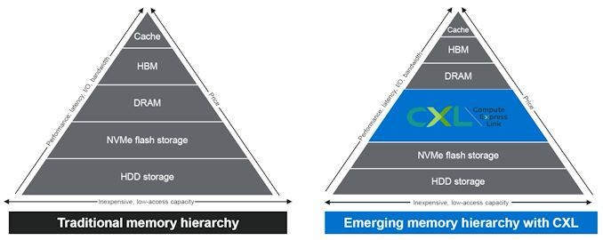
The migration of server platforms from DDR4 to DDR5, along with the rise of workloads demanding large RAM capacity (but not particularly sensitive to either memory bandwidth or latency), has opened up memory expansion modules as one of the first set of widely available CXL devices. Over the last couple of years, we have had product announcements from Samsung and Micron in this area.
At FMS 2024, SK hynix was showing off their DDR5-based CMM-DDR5 CXL memory module with a 128 GB capacity. The company was also detailing their associated Heterogeneous Memory Software Development Kit (HMSDK) - a set of libraries and tools at both the kernel and user levels aimed at increasing the ease of use of CXL memory. This is achieved in part by considering the memory pyramid / hierarchy and relocating the data between the server's main memory (DRAM) and the CXL device based on usage frequency.
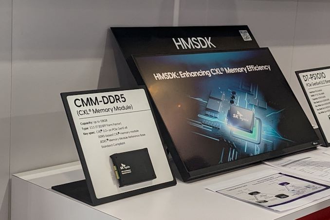
The CMM-DDR5 CXL memory module comes in the SDFF form-factor (E3.S 2T) with a PCIe 3.0 x8 host interface. The internal memory is based on 1α technology DRAM, and the device promises DDR5-class bandwidth and latency within a single NUMA hop. As these memory modules are meant to be used in datacenters and enterprises, the firmware includes features for RAS (reliability, availability, and serviceability) along with secure boot and other management features.
SK hynix was also demonstrating Niagara 2.0 - a hardware solution (currently based on FPGAs) to enable memory pooling and sharing - i.e, connecting multiple CXL memories to allow different hosts (CPUs and GPUs) to optimally share their capacity. The previous version only allowed capacity sharing, but the latest version enables sharing of data also. SK hynix had presented these solutions at the CXL DevCon 2024 earlier this year, but some progress seems to have been made in finalizing the specifications of the CMM-DDR5 at FMS 2024.
Micron had unveiled the CZ120 CXL Memory Expansion Module last year based on the Microchip SMC 2000 series CXL memory controller. At FMS 2024, Micron and Microchip had a demonstration of the module on a Granite Rapids server.
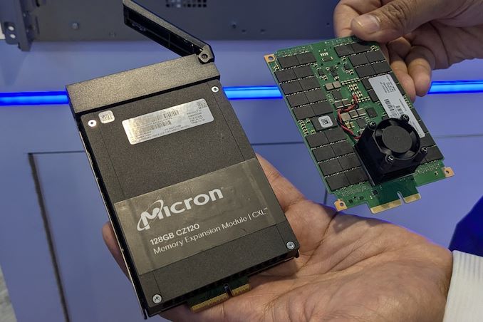
Additional insights into the SMC 2000 controller were also provided.
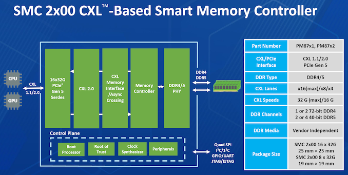
The CXL memory controller also incorporates DRAM die failure handling, and Microchip also provides diagnostics and debug tools to analyze failed modules. The memory controller also supports ECC, which forms part of the enterprise... Storage

Lorem Ipsum is simply dummy text of the printing and typesetting industry. Lorem Ipsum has been the industry's.
Samsung had quietly launched its BM1743 enterprise QLC SSD last month with a hefty 61.44 TB SKU. At FMS 2024, the company had the even larger 122.88 TB version of that SSD on display, alongside a few recorded benchmarking sessions. Compared to the previous generation, the BM1743 comes with a 4.1x improvement in I/O performance, improvement in data retention, and a 45% improvement in power efficiency for sequential writes.
The 128 TB-class QLC SSD boasts of sequential read speeds of 7.5 GBps and write speeds of 3 GBps. Random reads come in at 1.6 M IOPS, while 16 KB random writes clock in at 45K IOPS. Based on the quoted random write access granularity, it appears that Samsung is using a 16 KB indirection unit (IU) to optimize flash management. This is similar to the strategy adopted by Solidigm with IUs larger than 4K in their high-capacity SSDs.
A recorded benchmark session on the company's PM9D3a 8-channel Gen 5 SSD was also on display.
The SSD family is being promoted as a mainstream option for datacenters, and boasts of sequential reads up to 12 GBps and writes up to 6.8 GBps. Random reads clock in at 2 M IOPS, and random writes at 400 K IOPS.
Available in multiple form-factors up to 32 TB (M.2 tops out at 2 TB), the drive's firmware includes optional support for flexible data placement (FDP) to help address the write amplification aspect.
The PM1753 is the current enterprise SSD flagship in Samsung's lineup. With support for 16 NAND channels and capacities up to 32 TB, this U.2 / E3.S SSD has advertised sequential read and write speeds of 14.8 GBps and 11 GBps respectively. Random reads and writes for 4 KB accesses are listed at 3.4 M and 600 K IOPS.
Samsung claims a 1.7x performance improvement and a 1.7x power efficiency improvement over the previous generation (PM1743), making this TLC SSD suitable for AI servers.
The 9th Gen. V-NAND wafer was also available for viewing, though photography was prohibited. Mass production of this flash memory began in April 2024.
Storage
As the second quarter of 2024 is soon set to unfold, there are many things to be excited about, especially as Computex 2024 has been and gone. We now know that AMD's upcoming Ryzen 9000 series desktop processors using the new Zen 5 cores will be hitting shelves at the end of the month (31st July), and on top of this, AMD also recently slashed pricing on their Zen 4 (Ryzen 8000) processors. Intel still needs to follow suit with their 14th or 13th Gen Core series processors, but right now from a cost standpoint, AMD is in a much better position.
Since the publication of our last guide, the only notable CPU to be launched was Intel's special binned Core i9-14900KS, which not only pushes clock speeds up to 6.2 GHz but is the last processor to feature Intel's iconic Core I series nomenclature. The other big news in the CPU world was from Intel, with a statement issued about pushing users to use the Intel Default Specification on Intel's 14th and 13th Gen processors, which ultimately limits the performance compared to published data. We're still in the process of
While the CPU market has been relatively quiet so far this year, and things are set to pick up once AMD's Zen 5 and Intel's Arrow Lake desktop chips are all launched onto the market, it means today we are working for the same hymn sheet as our previous guide. With AMD's price drops on Ryzen 7000 series processors, much of the guide reflects this as AMD and Intel's performance is neck and neck in many use cases, but cost certainly plays a big factor in selecting a new CPU. As we move into the rest of 2024, the CPU market looks set to see the rise of the 'AI PC,' which is looking set to be something that many companies will focus on by the end of 2024, both on mobile and desktop platforms.
Guides
Samsung had quietly launched its BM1743 enterprise QLC SSD last month with a hefty 61.44 TB SKU. At FMS 2024, the company had the even larger 122.88 TB version of that SSD on display, alongside a few recorded benchmarking sessions. Compared to the previous generation, the BM1743 comes with a 4.1x improvement in I/O performance, improvement in data retention, and a 45% improvement in power efficiency for sequential writes.
The 128 TB-class QLC SSD boasts of sequential read speeds of 7.5 GBps and write speeds of 3 GBps. Random reads come in at 1.6 M IOPS, while 16 KB random writes clock in at 45K IOPS. Based on the quoted random write access granularity, it appears that Samsung is using a 16 KB indirection unit (IU) to optimize flash management. This is similar to the strategy adopted by Solidigm with IUs larger than 4K in their high-capacity SSDs.
A recorded benchmark session on the company's PM9D3a 8-channel Gen 5 SSD was also on display.
The SSD family is being promoted as a mainstream option for datacenters, and boasts of sequential reads up to 12 GBps and writes up to 6.8 GBps. Random reads clock in at 2 M IOPS, and random writes at 400 K IOPS.
Available in multiple form-factors up to 32 TB (M.2 tops out at 2 TB), the drive's firmware includes optional support for flexible data placement (FDP) to help address the write amplification aspect.
The PM1753 is the current enterprise SSD flagship in Samsung's lineup. With support for 16 NAND channels and capacities up to 32 TB, this U.2 / E3.S SSD has advertised sequential read and write speeds of 14.8 GBps and 11 GBps respectively. Random reads and writes for 4 KB accesses are listed at 3.4 M and 600 K IOPS.
Samsung claims a 1.7x performance improvement and a 1.7x power efficiency improvement over the previous generation (PM1743), making this TLC SSD suitable for AI servers.
The 9th Gen. V-NAND wafer was also available for viewing, though photography was prohibited. Mass production of this flash memory began in April 2024.
Storage
 operating model, but never has it been so risky at it is for the already weakened Intel.</p>
<p>Intel’s do-or-die dash for process leadership means that, for the next 18 months or so, all eyes are on the company’s 20A and 18A process nodes. The final nodes in their ambitious 5 Nodes in 4 Years roadmap, the twinned 20A/18A are the culmination of several new technologies, primarily Intel’s GAAFET implementation (RibbonFET), which is being combined with PowerVia, Intel’s backside power delivery network (BS-PDN) technology. 20A is set to serve as Intel’s early version of the node, and 18A the refined version for long-term use both internally, and as the first major external node for Intel Foundry. To say that everything rides on Intel 18A isn’t quite accurate, but it’s only a slight embellishment.</p>
<p>To that end, we’re going to see Intel deliver a lot of status updates on 18A over the next year as they continue to outline to investors and external customers alike that they have the manufacturing side of their business in order. And today is one of those days, with a fresh update on the state of 18A.</p>
<h3>18A Chips Back & Booting</h3>
<p>So what’s new with 18A? The biggest news out of Intel this morning is that their first 18A chips are back from the development fab and are successfully booting operating systems. This means the silicon not only works (power-on), but works well enough to complete core tasks. It’s a major step in bringing up a chip, and at this point, Intel wants to make sure to let the whole world know.</p>
<p align="center"><a href="https://www.anandtech.com/show/21504/intel-18a-status-update-first-chips-booting-first-external-customer-tapeout-in-h125"><img alt="" src="https://images.anandtech.com/doci/21504/2024-Q3-Progress-on-Foundry_18A_Aug62024.png" style="width: 100%;" /></a></p>
<p>Earlier this year the company finished taping out both of its lead 18A chips: <a href="https://www.anandtech.com/show/21430/update-on-intel-s-panther-lake-at-computex-2024-intel-powering-up-intel-18a-wafer-next-week">Panther Lake</a> for clients, and <a href="https://www.anandtech.com/show/18797/intel-updates-data-center-roadmap-xeons-on-track-emerald-in-q423-sierra-forest-in-h124">Clearwater Forest</a> for servers. And it’s both chips that are booting. This is made all the more significant by the fact that Clearwater Forest also relies on Intel’s die-to-die hybrid bonding packaging technology, Foveros Direct 3D, where it will be the lead product for that technology as well. Which for Intel, is a promising sign that not only are their silicon lithography ambitions paying off, but their intention to lead in advanced packaging is on-track as well.</p>
<p>And while Intel doesn’t normally talk about yields this early in the game, it’s interesting to note that in a separate Q&A being published this morning with Intel Foundry’s new boss, <a href="https://www.intel.com/content/www/us/en/newsroom/news/kevin-obuckley-talks-progress-intel-18a.html">Kevin O’Buckley</a>, the head of Foundry Services explicitly comments that Panther Lake is “yielding well”. Similarly, Panther Lake’s DDR memory controller (a complex block mixing logic with a PHY) is already running at its target frequency. Progress is going so well, apparently, that according to O’Buckley, it’s ahead of schedule on its product qualification milestones.</p>
<h3>PDK 1.0 Released, First External Customer Tape-Out Expected in H1’25</h3>
<p>As for Intel’s contract foundry business, the company is ramping up its efforts there now that the first full process design kit (PDK) is ready for 18A. Intel released their 18A PDK 1.0 last month, giving Intel’s customers (and potential customers) the tools to finally finish designing their chips for production. As is typically the case of a new node, pre-release PDKs were available for companies to get start... CPUs)
 operating model, but never has it been so risky at it is for the already weakened Intel.</p>
<p>Intel’s do-or-die dash for process leadership means that, for the next 18 months or so, all eyes are on the company’s 20A and 18A process nodes. The final nodes in their ambitious 5 Nodes in 4 Years roadmap, the twinned 20A/18A are the culmination of several new technologies, primarily Intel’s GAAFET implementation (RibbonFET), which is being combined with PowerVia, Intel’s backside power delivery network (BS-PDN) technology. 20A is set to serve as Intel’s early version of the node, and 18A the refined version for long-term use both internally, and as the first major external node for Intel Foundry. To say that everything rides on Intel 18A isn’t quite accurate, but it’s only a slight embellishment.</p>
<p>To that end, we’re going to see Intel deliver a lot of status updates on 18A over the next year as they continue to outline to investors and external customers alike that they have the manufacturing side of their business in order. And today is one of those days, with a fresh update on the state of 18A.</p>
<h3>18A Chips Back & Booting</h3>
<p>So what’s new with 18A? The biggest news out of Intel this morning is that their first 18A chips are back from the development fab and are successfully booting operating systems. This means the silicon not only works (power-on), but works well enough to complete core tasks. It’s a major step in bringing up a chip, and at this point, Intel wants to make sure to let the whole world know.</p>
<p align="center"><a href="https://www.anandtech.com/show/21504/intel-18a-status-update-first-chips-booting-first-external-customer-tapeout-in-h125"><img alt="" src="https://images.anandtech.com/doci/21504/2024-Q3-Progress-on-Foundry_18A_Aug62024.png" style="width: 100%;" /></a></p>
<p>Earlier this year the company finished taping out both of its lead 18A chips: <a href="https://www.anandtech.com/show/21430/update-on-intel-s-panther-lake-at-computex-2024-intel-powering-up-intel-18a-wafer-next-week">Panther Lake</a> for clients, and <a href="https://www.anandtech.com/show/18797/intel-updates-data-center-roadmap-xeons-on-track-emerald-in-q423-sierra-forest-in-h124">Clearwater Forest</a> for servers. And it’s both chips that are booting. This is made all the more significant by the fact that Clearwater Forest also relies on Intel’s die-to-die hybrid bonding packaging technology, Foveros Direct 3D, where it will be the lead product for that technology as well. Which for Intel, is a promising sign that not only are their silicon lithography ambitions paying off, but their intention to lead in advanced packaging is on-track as well.</p>
<p>And while Intel doesn’t normally talk about yields this early in the game, it’s interesting to note that in a separate Q&A being published this morning with Intel Foundry’s new boss, <a href="https://www.intel.com/content/www/us/en/newsroom/news/kevin-obuckley-talks-progress-intel-18a.html">Kevin O’Buckley</a>, the head of Foundry Services explicitly comments that Panther Lake is “yielding well”. Similarly, Panther Lake’s DDR memory controller (a complex block mixing logic with a PHY) is already running at its target frequency. Progress is going so well, apparently, that according to O’Buckley, it’s ahead of schedule on its product qualification milestones.</p>
<h3>PDK 1.0 Released, First External Customer Tape-Out Expected in H1’25</h3>
<p>As for Intel’s contract foundry business, the company is ramping up its efforts there now that the first full process design kit (PDK) is ready for 18A. Intel released their 18A PDK 1.0 last month, giving Intel’s customers (and potential customers) the tools to finally finish designing their chips for production. As is typically the case of a new node, pre-release PDKs were available for companies to get start... CPUs | https://compbuddey.blogspot.com/2024/08/intel-18a-status-update-first-chips_18.html)
 operating model, but never has it been so risky at it is for the already weakened Intel.</p>
<p>Intel’s do-or-die dash for process leadership means that, for the next 18 months or so, all eyes are on the company’s 20A and 18A process nodes. The final nodes in their ambitious 5 Nodes in 4 Years roadmap, the twinned 20A/18A are the culmination of several new technologies, primarily Intel’s GAAFET implementation (RibbonFET), which is being combined with PowerVia, Intel’s backside power delivery network (BS-PDN) technology. 20A is set to serve as Intel’s early version of the node, and 18A the refined version for long-term use both internally, and as the first major external node for Intel Foundry. To say that everything rides on Intel 18A isn’t quite accurate, but it’s only a slight embellishment.</p>
<p>To that end, we’re going to see Intel deliver a lot of status updates on 18A over the next year as they continue to outline to investors and external customers alike that they have the manufacturing side of their business in order. And today is one of those days, with a fresh update on the state of 18A.</p>
<h3>18A Chips Back & Booting</h3>
<p>So what’s new with 18A? The biggest news out of Intel this morning is that their first 18A chips are back from the development fab and are successfully booting operating systems. This means the silicon not only works (power-on), but works well enough to complete core tasks. It’s a major step in bringing up a chip, and at this point, Intel wants to make sure to let the whole world know.</p>
<p align="center"><a href="https://www.anandtech.com/show/21504/intel-18a-status-update-first-chips-booting-first-external-customer-tapeout-in-h125"><img alt="" src="https://images.anandtech.com/doci/21504/2024-Q3-Progress-on-Foundry_18A_Aug62024.png" style="width: 100%;" /></a></p>
<p>Earlier this year the company finished taping out both of its lead 18A chips: <a href="https://www.anandtech.com/show/21430/update-on-intel-s-panther-lake-at-computex-2024-intel-powering-up-intel-18a-wafer-next-week">Panther Lake</a> for clients, and <a href="https://www.anandtech.com/show/18797/intel-updates-data-center-roadmap-xeons-on-track-emerald-in-q423-sierra-forest-in-h124">Clearwater Forest</a> for servers. And it’s both chips that are booting. This is made all the more significant by the fact that Clearwater Forest also relies on Intel’s die-to-die hybrid bonding packaging technology, Foveros Direct 3D, where it will be the lead product for that technology as well. Which for Intel, is a promising sign that not only are their silicon lithography ambitions paying off, but their intention to lead in advanced packaging is on-track as well.</p>
<p>And while Intel doesn’t normally talk about yields this early in the game, it’s interesting to note that in a separate Q&A being published this morning with Intel Foundry’s new boss, <a href="https://www.intel.com/content/www/us/en/newsroom/news/kevin-obuckley-talks-progress-intel-18a.html">Kevin O’Buckley</a>, the head of Foundry Services explicitly comments that Panther Lake is “yielding well”. Similarly, Panther Lake’s DDR memory controller (a complex block mixing logic with a PHY) is already running at its target frequency. Progress is going so well, apparently, that according to O’Buckley, it’s ahead of schedule on its product qualification milestones.</p>
<h3>PDK 1.0 Released, First External Customer Tape-Out Expected in H1’25</h3>
<p>As for Intel’s contract foundry business, the company is ramping up its efforts there now that the first full process design kit (PDK) is ready for 18A. Intel released their 18A PDK 1.0 last month, giving Intel’s customers (and potential customers) the tools to finally finish designing their chips for production. As is typically the case of a new node, pre-release PDKs were available for companies to get start... CPUs&body=https://compbuddey.blogspot.com/2024/08/intel-18a-status-update-first-chips_18.html)
0 Comments