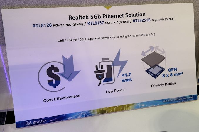

One of the more subtle trends at this year's Computex was that the majority of high-end motherboards now come equipped with a 5GbE network controller. At present, this might be considered a limited benefit as 5GbE and 10GbE switches and routers are still pretty expensive. But Realtek is planning on tackling the issue from both ends, as the company is preparing a hardware platform for sub-$100 5GbE switches.
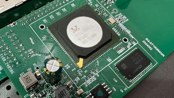
Realtek’s quad-port 5GbE switch platform consists of five key chips: one RTL9303 switch system-on-chip, and four RTL8251B 5GbE physical interfaces (PHYs). The chips are accompanied by various other components, such as power management ICs, but in general it relies solely on in-house developed components, which is why it can be made so cheap.
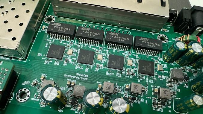
RealTek's platform is meant for home and small offices, which is reflected in the switch's feature set. This is a simple, unmanaged switch with a handful of ports, making it ideal for linking up a few systems, while enterprise users will likely find it a bit too basic.
Segmenting the market like this is ultimately critical for bringing down the price of hardware. The bulk of 5GbE/10GbE switches on the market today are more enterprise-focused managed switches, which carry more features and a price premium to match. So developing a stripped-down platform for cheaper consumer switches is a huge development that should finally make it economical for consumers to adopt faster networking hardware, similar to 2.5GbE a few years ago.
At present, 2.5GbE switches are running at around $20/port, so RealTek's sub-$100 target for a 4-port switch aims to bring 5GbE in at just a slightly higher price tag of $25/port. Or, compared to the handful of unmanaged 10GbE switches on the market, which average $60/port, this will be less than half the price (though at half the bandwidth).
The proliferation of cheap 5GbE network switches will also mark a notable inflection point in Ethernet hardware design, as it's the fastest standard that is rated to work the ubiquitous Cat 5e cable. The NBASE-T standard was penned almost a decade ago in order to cover the missing-middle between 1GbE and 10GbE, while getting more bandwidth out of existing, widely-deployed Cat 5e cabling. So with the release of consumer 5GbE gear, the standard's goals are finally coming to fruition – though it does mean we're finally reaching the end of the road for the oldest network cabling still widely in use.
For now, Realtek is only talking about one customer offering a sub-$100 5GbE switch this September, but something tells me that other partners of the company will come up with similar devices soon enough. As a result of the competition, prices could get even lower, which is always good for buyers.
These benefits should also funnel into Wi-Fi 7 routers, to a limited extent. Wired backhaul speeds need to keep pace with ever-faster Wi-Fi standards in order to keep those newer radios fed, so it's not a coincidence that cheaper 5GbE is finally coming right as Wi-Fi 7 is taking off.
Overall, the company's 5GbE switch platform is part of a larger ecosystem of 5GbE hardware that Realtek was showing off at Computex. In addition to RTL8251B 5GbE PHYs and RTL9303 switch SoC, the company is also preparing their RTL8126 PCIe 3.1 network controller, and RTL8157 NIC for USB dongles.
Networking
Standard CPU coolers, while adequate for managing basic thermal loads, often fall short in terms of noise reduction and superior cooling efficiency. This limitation drives advanced users and system builders to seek aftermarket solutions tailored to their specific needs. The high-end aftermarket cooler market is highly competitive, with manufacturers striving to offer products with exceptional performance.
Endorfy, previously known as SilentiumPC, is a Polish manufacturer that has undergone a significant transformation to expand its presence in global markets. The brand is known for delivering high-performance cooling solutions with a strong focus on balancing efficiency and affordability. By rebranding as Endorfy, the company aims to enter premium market segments while continuing to offer reliable, high-quality cooling products.
SilentiumPC became very popular in the value/mainstream segments of the PC market with their products, the spearhead of which probably was the Fera 5 cooler that we reviewed a little over two years ago and had a remarkable value for money. Today’s review places Endorfy’s largest CPU cooler, the Fortis 5 Dual Fan, on our laboratory test bench. The Fortis 5 is the largest CPU air cooler the company currently offers and is significantly more expensive than the Fera 5, yet it still is a single-tower cooler that strives to strike a balance between value, compatibility, and performance.
Cases/Cooling/PSUs![Micron: U.S. Fabs Will Start Operating in 2026 - 2029 <p align="center"><a href="https://www.anandtech.com/show/21459/micron-u-s-fabs-will-start-operating-in-2026-2029"><img src="https://images.anandtech.com/doci/21459/micron-server-datacenter-general-generic-678_575px.jpg" alt="" /></a></p><p><p>When Micron announced plans to build two new fabs in the U.S. in 2022, the company vaguely said both would come online by the decade's end. Then, in 2023, it began to optimize its spending, which pushed production at these fabrication facilities. This week, the company outlined more precise timeframes for when its fabs in <a href="https://www.anandtech.com/show/17573/micron-breaks-ground-on-its-15-billion-euv-dram-fab-in-the-us">Idaho</a> and <a href="https://www.anandtech.com/show/17606/micron-announces-100-billion-us-fab-complex-a-20year-plan">New York</a> will start operations: this will happen from calendar 2026 to calendar 2029.</p>
<p>"<em>These fab construction investments are necessary to support supply growth for the latter half of this decade,</em>" a statement by Micron in its Q3 FY2024 financial results report <a href="https://investors.micron.com/static-files/a531c7f0-fca2-48f3-8f24-79c945aaa2d2">reads</a>. "<em>This Idaho fab will not contribute to meaningful bit supply until fiscal 2027 and the New York construction capex is not expected to contribute to bit supply growth until fiscal 2028 or later. The timing of future [wafer fab equipment] spend in these fabs will be managed to align supply growth with expected demand growth.</em>"</p>
<p>Micron's fiscal year 2027 starts in September 2026, so the new fab near Boise, Idaho, is set to start operations between September 2026 and September 2027. The company's fiscal 2028 starts in September 2027, so the fab will likely begin operations in calendar 2028 or later, probably depending on the demand for DRAM memory in the coming years. That said, Micron's U.S. memory fabs will begin operations between late 2026 and 2029, which aligns with the company's original plans. </p>
<p>Construction of the fab in Idaho is well underway. In contrast, construction of the New York facility has yet to begin as the company is working on regulatory and permitting processes in the state. </p>
<p>Micron's capital expenditure (CaPex) plan for FY2024 is approximately $8.0 billion, with a decrease in year-over-year spending on wafer fabrication equipment (WFE). In Q4 FY2024, the company will spend around $3 billion on fab construction, new wafer fab tools, and various expansions/upgrades.</p>
<p>Looking ahead to FY2025, the company plans a substantial increase in capex, targeting a mid-30s percentage of revenue to support various technological and facility advancements. In particular, it expects its quarterly CapEx to average above the $3 billion level seen in the fourth quarter of FY2024, which means that it plans to spend about $12 billion in its fiscal 2025, which begins in late September.</p>
<p>Half or more of the total CapEx increase in FY2025 (i.e., over $2 billion) will be allocated to constructing new fabs in Idaho and New York. Meanwhile, the FY2025 CapEx will significantly rise to fund high-bandwidth memory (HBM) assembly and testing and the construction of fabrication and back-end facilities. This increase also includes investments in technology transitions to meet growing demand. </p>
<p>"<em>Fab construction in Idaho is underway, and we are working diligently to complete the regulatory and permitting processes in New York,</em>" said Sanjay Mehrotra, chief executive officer of Micron, at the company's conference call with investors and financial analysts (via <a href="https://seekingalpha.com/article/4701253-micron-technology-inc-mu-q3-2024-earnings-call-transcript?source=content_type%3Areact%7Csection%3ATranscripts%7Csection_asset%3ATranscripts%7Cfirst_level_url%3Asymbol%7Cbutton%3ATitle%7Clock_status%3ANo%7Cline%3A1">SeekingAlpha</a>). "<em>This additional leading-edge greenfield capacity, along with continued technology transition investments in our Asia facilities, is required to meet long-term demand in the second half of this decade and beyond. These investments support our objective to maintain our current bit share over time and to grow our memory bit supply in line with long-term industry bit demand.</em>"</p>
</p> Memory](https://lh3.googleusercontent.com/blogger_img_proxy/AEn0k_snvK5kTgDIQFPG_HAO1-qSKgAAd0s8SsUEXY0bEhhgBFWdMS41vs1dcZnk0LI4qltznSgyN1qC0MmhsGBtOjAxdr7yZkawNCXj9eITxkwfNXdQp3LanILGbK_jCDoxVcYE9YzDq6D93cVMMKhKjGfLKNoJRs-0wro_REFkkmeoNto=w72-h72-p-k-no-nu)

When Micron announced plans to build two new fabs in the U.S. in 2022, the company vaguely said both would come online by the decade's end. Then, in 2023, it began to optimize its spending, which pushed production at these fabrication facilities. This week, the company outlined more precise timeframes for when its fabs in Idaho and New York will start operations: this will happen from calendar 2026 to calendar 2029.
"These fab construction investments are necessary to support supply growth for the latter half of this decade," a statement by Micron in its Q3 FY2024 financial results report reads. "This Idaho fab will not contribute to meaningful bit supply until fiscal 2027 and the New York construction capex is not expected to contribute to bit supply growth until fiscal 2028 or later. The timing of future [wafer fab equipment] spend in these fabs will be managed to align supply growth with expected demand growth."
Micron's fiscal year 2027 starts in September 2026, so the new fab near Boise, Idaho, is set to start operations between September 2026 and September 2027. The company's fiscal 2028 starts in September 2027, so the fab will likely begin operations in calendar 2028 or later, probably depending on the demand for DRAM memory in the coming years. That said, Micron's U.S. memory fabs will begin operations between late 2026 and 2029, which aligns with the company's original plans.
Construction of the fab in Idaho is well underway. In contrast, construction of the New York facility has yet to begin as the company is working on regulatory and permitting processes in the state.
Micron's capital expenditure (CaPex) plan for FY2024 is approximately $8.0 billion, with a decrease in year-over-year spending on wafer fabrication equipment (WFE). In Q4 FY2024, the company will spend around $3 billion on fab construction, new wafer fab tools, and various expansions/upgrades.
Looking ahead to FY2025, the company plans a substantial increase in capex, targeting a mid-30s percentage of revenue to support various technological and facility advancements. In particular, it expects its quarterly CapEx to average above the $3 billion level seen in the fourth quarter of FY2024, which means that it plans to spend about $12 billion in its fiscal 2025, which begins in late September.
Half or more of the total CapEx increase in FY2025 (i.e., over $2 billion) will be allocated to constructing new fabs in Idaho and New York. Meanwhile, the FY2025 CapEx will significantly rise to fund high-bandwidth memory (HBM) assembly and testing and the construction of fabrication and back-end facilities. This increase also includes investments in technology transitions to meet growing demand.
"Fab construction in Idaho is underway, and we are working diligently to complete the regulatory and permitting processes in New York," said Sanjay Mehrotra, chief executive officer of Micron, at the company's conference call with investors and financial analysts (via SeekingAlpha). "This additional leading-edge greenfield capacity, along with continued technology transition investments in our Asia facilities, is required to meet long-term demand in the second half of this decade and beyond. These investments support our objective to maintain our current bit share over time and to grow our memory bit supply in line with long-term industry bit demand."
Memory

Kioxia's booth at FMS 2024 was a busy one with multiple technology demonstrations keeping visitors occupied. A walk-through of the BiCS 8 manufacturing process was the first to grab my attention. Kioxia and Western Digital announced the sampling of BiCS 8 in March 2023. We had touched briefly upon its CMOS Bonded Array (CBA) scheme in our coverage of Kioxial's 2Tb QLC NAND device and coverage of Western Digital's 128 TB QLC enterprise SSD proof-of-concept demonstration. At Kioxia's booth, we got more insights.

Traditionally, fabrication of flash chips involved placement of the associate logic circuitry (CMOS process) around the periphery of the flash array. The process then moved on to putting the CMOS under the cell array, but the wafer development process was serialized with the CMOS logic getting fabricated first followed by the cell array on top. However, this has some challenges because the cell array requires a high-temperature processing step to ensure higher reliability that can be detrimental to the health of the CMOS logic. Thanks to recent advancements in wafer bonding techniques, the new CBA process allows the CMOS wafer and cell array wafer to be processed independently in parallel and then pieced together, as shown in the models above.

The BiCS 8 3D NAND incorporates 218 layers, compared to 112 layers in BiCS 5 and 162 layers in BiCS 6. The company decided to skip over BiCS 7 (or, rather, it was probably a short-lived generation meant as an internal test vehicle). The generation retains the four-plane charge trap structure of BiCS 6. In its TLC avatar, it is available as a 1 Tbit device. The QLC version is available in two capacities - 1 Tbit and 2 Tbit.
Kioxia also noted that while the number of layers (218) doesn't compare favorably with the latest layer counts from the competition, its lateral scaling / cell shrinkage has enabled it to be competitive in terms of bit density as well as operating speeds (3200 MT/s). For reference, the latest shipping NAND from Micron - the G9 - has 276 layers with a bit density in TLC mode of 21 Gbit/mm2, and operates at up to 3600 MT/s. However, its 232L NAND operates only up to 2400 MT/s and has a bit density of 14.6 Gbit/mm2.
It must be noted that the CBA hybrid bonding process has advantages over the current processes used by other vendors - including Micron's CMOS under array (CuA) and SK hynix's 4D PUC (periphery-under-chip) developed in the late 2010s. It is expected that other NAND vendors will also move eventually to some variant of the hybrid bonding scheme used by Kioxia.
Storage
Lorem Ipsum is simply dummy text of the printing and typesetting industry. Lorem Ipsum has been the industry's.


. The chips are accompanied by various other components, such as power management ICs, but in general it relies solely on in-house developed components, which is why it can be made so cheap. </p>
<p style="text-align: center;"><a href="https://www.anandtech.com/show/21449/realtek-has-a-platform-for-sub100-5gbe-switch"><img alt="" src="https://images.anandtech.com/doci/21449/IMG_0075-phy_575px.jpg" /></a></p>
<p>RealTek's platform is meant for home and small offices, which is reflected in the switch's feature set. This is a simple, unmanaged switch with a handful of ports, making it ideal for linking up a few systems, while enterprise users will likely find it a bit too basic.</p>
<p>Segmenting the market like this is ultimately critical for bringing down the price of hardware. The bulk of 5GbE/10GbE switches on the market today are more enterprise-focused managed switches, which carry more features and a price premium to match. So developing a stripped-down platform for cheaper consumer switches is a huge development that should finally make it economical for consumers to adopt faster networking hardware, similar to 2.5GbE a few years ago.</p>
<p>At present, 2.5GbE switches are running at around $20/port, so RealTek's sub-$100 target for a 4-port switch aims to bring 5GbE in at just a slightly higher price tag of $25/port. Or, compared to the handful of unmanaged 10GbE switches on the market, which average $60/port, this will be less than half the price (though at half the bandwidth).</p>
<p>The proliferation of cheap 5GbE network switches will also mark a notable inflection point in Ethernet hardware design, as it's the fastest standard that is rated to work the ubiquitous Cat 5e cable. The NBASE-T standard was penned almost a decade ago in order to cover the missing-middle between 1GbE and 10GbE, while getting more bandwidth out of existing, widely-deployed Cat 5e cabling. So with the release of consumer 5GbE gear, the standard's goals are finally coming to fruition – though it does mean we're finally reaching the end of the road for the oldest network cabling still widely in use.</p>
<p style="text-align: center;"><a href="https://www.anandtech.com/show/21449/realtek-has-a-platform-for-sub100-5gbe-switch"><img alt="" src="https://images.anandtech.com/doci/21449/IMG_0074-realtek-chip_575px.jpg" /></a></p>
<p>For now, Realtek is only talking about one customer offering a sub-$100 5GbE switch this September, but something tells me that other partners of the company will come up with similar devices soon enough. As a result of the competition, prices could get even lower, which is always good for buyers.</p>
<p>These benefits should also funnel into Wi-Fi 7 routers, to a limited extent. Wired backhaul speeds need to keep pace with ever-faster Wi-Fi standards in order to keep those newer radios fed, so it's not a coincidence that cheaper 5GbE is finally coming right as Wi-Fi 7 is taking off.</p>
<p>Overall, the company's 5GbE switch platform is part of a larger ecosystem of 5GbE hardware that Realtek was showing off at Computex. In addition to RTL8251B 5GbE PHYs and RTL9303 switch SoC, the company is also preparing their RTL8126 PCIe 3.1 network controller, and RTL8157 NIC for USB dongles.</p>
</p> Networking)
. The chips are accompanied by various other components, such as power management ICs, but in general it relies solely on in-house developed components, which is why it can be made so cheap. </p>
<p style="text-align: center;"><a href="https://www.anandtech.com/show/21449/realtek-has-a-platform-for-sub100-5gbe-switch"><img alt="" src="https://images.anandtech.com/doci/21449/IMG_0075-phy_575px.jpg" /></a></p>
<p>RealTek's platform is meant for home and small offices, which is reflected in the switch's feature set. This is a simple, unmanaged switch with a handful of ports, making it ideal for linking up a few systems, while enterprise users will likely find it a bit too basic.</p>
<p>Segmenting the market like this is ultimately critical for bringing down the price of hardware. The bulk of 5GbE/10GbE switches on the market today are more enterprise-focused managed switches, which carry more features and a price premium to match. So developing a stripped-down platform for cheaper consumer switches is a huge development that should finally make it economical for consumers to adopt faster networking hardware, similar to 2.5GbE a few years ago.</p>
<p>At present, 2.5GbE switches are running at around $20/port, so RealTek's sub-$100 target for a 4-port switch aims to bring 5GbE in at just a slightly higher price tag of $25/port. Or, compared to the handful of unmanaged 10GbE switches on the market, which average $60/port, this will be less than half the price (though at half the bandwidth).</p>
<p>The proliferation of cheap 5GbE network switches will also mark a notable inflection point in Ethernet hardware design, as it's the fastest standard that is rated to work the ubiquitous Cat 5e cable. The NBASE-T standard was penned almost a decade ago in order to cover the missing-middle between 1GbE and 10GbE, while getting more bandwidth out of existing, widely-deployed Cat 5e cabling. So with the release of consumer 5GbE gear, the standard's goals are finally coming to fruition – though it does mean we're finally reaching the end of the road for the oldest network cabling still widely in use.</p>
<p style="text-align: center;"><a href="https://www.anandtech.com/show/21449/realtek-has-a-platform-for-sub100-5gbe-switch"><img alt="" src="https://images.anandtech.com/doci/21449/IMG_0074-realtek-chip_575px.jpg" /></a></p>
<p>For now, Realtek is only talking about one customer offering a sub-$100 5GbE switch this September, but something tells me that other partners of the company will come up with similar devices soon enough. As a result of the competition, prices could get even lower, which is always good for buyers.</p>
<p>These benefits should also funnel into Wi-Fi 7 routers, to a limited extent. Wired backhaul speeds need to keep pace with ever-faster Wi-Fi standards in order to keep those newer radios fed, so it's not a coincidence that cheaper 5GbE is finally coming right as Wi-Fi 7 is taking off.</p>
<p>Overall, the company's 5GbE switch platform is part of a larger ecosystem of 5GbE hardware that Realtek was showing off at Computex. In addition to RTL8251B 5GbE PHYs and RTL9303 switch SoC, the company is also preparing their RTL8126 PCIe 3.1 network controller, and RTL8157 NIC for USB dongles.</p>
</p> Networking | https://compbuddey.blogspot.com/2024/07/realtek-previews-platform-for-sub-100_29.html)
. The chips are accompanied by various other components, such as power management ICs, but in general it relies solely on in-house developed components, which is why it can be made so cheap. </p>
<p style="text-align: center;"><a href="https://www.anandtech.com/show/21449/realtek-has-a-platform-for-sub100-5gbe-switch"><img alt="" src="https://images.anandtech.com/doci/21449/IMG_0075-phy_575px.jpg" /></a></p>
<p>RealTek's platform is meant for home and small offices, which is reflected in the switch's feature set. This is a simple, unmanaged switch with a handful of ports, making it ideal for linking up a few systems, while enterprise users will likely find it a bit too basic.</p>
<p>Segmenting the market like this is ultimately critical for bringing down the price of hardware. The bulk of 5GbE/10GbE switches on the market today are more enterprise-focused managed switches, which carry more features and a price premium to match. So developing a stripped-down platform for cheaper consumer switches is a huge development that should finally make it economical for consumers to adopt faster networking hardware, similar to 2.5GbE a few years ago.</p>
<p>At present, 2.5GbE switches are running at around $20/port, so RealTek's sub-$100 target for a 4-port switch aims to bring 5GbE in at just a slightly higher price tag of $25/port. Or, compared to the handful of unmanaged 10GbE switches on the market, which average $60/port, this will be less than half the price (though at half the bandwidth).</p>
<p>The proliferation of cheap 5GbE network switches will also mark a notable inflection point in Ethernet hardware design, as it's the fastest standard that is rated to work the ubiquitous Cat 5e cable. The NBASE-T standard was penned almost a decade ago in order to cover the missing-middle between 1GbE and 10GbE, while getting more bandwidth out of existing, widely-deployed Cat 5e cabling. So with the release of consumer 5GbE gear, the standard's goals are finally coming to fruition – though it does mean we're finally reaching the end of the road for the oldest network cabling still widely in use.</p>
<p style="text-align: center;"><a href="https://www.anandtech.com/show/21449/realtek-has-a-platform-for-sub100-5gbe-switch"><img alt="" src="https://images.anandtech.com/doci/21449/IMG_0074-realtek-chip_575px.jpg" /></a></p>
<p>For now, Realtek is only talking about one customer offering a sub-$100 5GbE switch this September, but something tells me that other partners of the company will come up with similar devices soon enough. As a result of the competition, prices could get even lower, which is always good for buyers.</p>
<p>These benefits should also funnel into Wi-Fi 7 routers, to a limited extent. Wired backhaul speeds need to keep pace with ever-faster Wi-Fi standards in order to keep those newer radios fed, so it's not a coincidence that cheaper 5GbE is finally coming right as Wi-Fi 7 is taking off.</p>
<p>Overall, the company's 5GbE switch platform is part of a larger ecosystem of 5GbE hardware that Realtek was showing off at Computex. In addition to RTL8251B 5GbE PHYs and RTL9303 switch SoC, the company is also preparing their RTL8126 PCIe 3.1 network controller, and RTL8157 NIC for USB dongles.</p>
</p> Networking&body=https://compbuddey.blogspot.com/2024/07/realtek-previews-platform-for-sub-100_29.html)
0 Comments