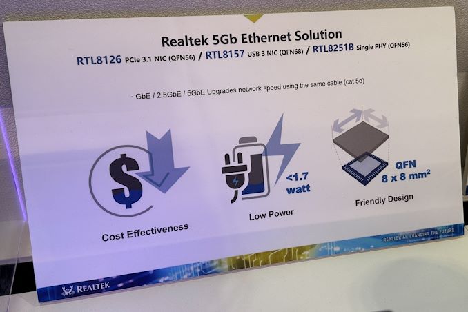

One of the more subtle trends at this year's Computex was that the majority of high-end motherboards now come equipped with a 5GbE network controller. At present, this might be considered a limited benefit as 5GbE and 10GbE switches and routers are still pretty expensive. But Realtek is planning on tackling the issue from both ends, as the company is preparing a hardware platform for sub-$100 5GbE switches.
Realtek’s quad-port 5GbE switch platform consists of five key chips: one RTL9303 switch system-on-chip, and four RTL8251B 5GbE physical interfaces (PHYs). The chips are accompanied by various other components, such as power management ICs, but in general it relies solely on in-house developed components, which is why it can be made so cheap.
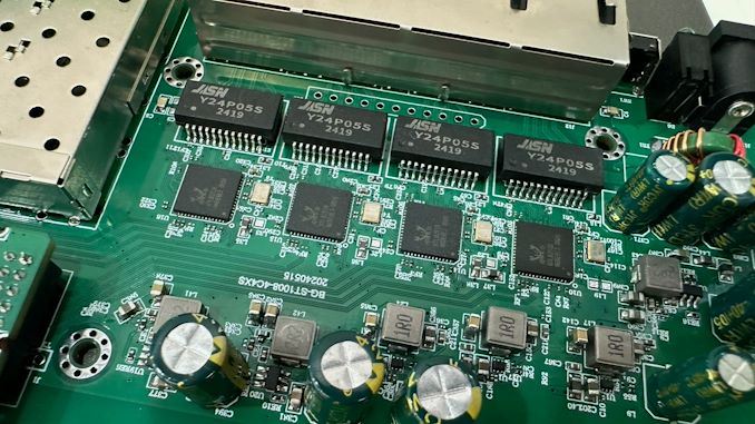
RealTek's platform is meant for home and small offices, which is reflected in the switch's feature set. This is a simple, unmanaged switch with a handful of ports, making it ideal for linking up a few systems, while enterprise users will likely find it a bit too basic.
Segmenting the market like this is ultimately critical for bringing down the price of hardware. The bulk of 5GbE/10GbE switches on the market today are more enterprise-focused managed switches, which carry more features and a price premium to match. So developing a stripped-down platform for cheaper consumer switches is a huge development that should finally make it economical for consumers to adopt faster networking hardware, similar to 2.5GbE a few years ago.
At present, 2.5GbE switches are running at around $20/port, so RealTek's sub-$100 target for a 4-port switch aims to bring 5GbE in at just a slightly higher price tag of $25/port. Or, compared to the handful of unmanaged 10GbE switches on the market, which average $60/port, this will be less than half the price (though at half the bandwidth).
The proliferation of cheap 5GbE network switches will also mark a notable inflection point in Ethernet hardware design, as it's the fastest standard that is rated to work the ubiquitous Cat 5e cable. The NBASE-T standard was penned almost a decade ago in order to cover the missing-middle between 1GbE and 10GbE, while getting more bandwidth out of existing, widely-deployed Cat 5e cabling. So with the release of consumer 5GbE gear, the standard's goals are finally coming to fruition – though it does mean we're finally reaching the end of the road for the oldest network cabling still widely in use.
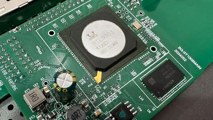
For now, Realtek is only talking about one customer offering a sub-$100 5GbE switch this September, but something tells me that other partners of the company will come up with similar devices soon enough. As a result of the competition, prices could get even lower, which is always good for buyers.
These benefits should also funnel into Wi-Fi 7 routers, to a limited extent. Wired backhaul speeds need to keep pace with ever-faster Wi-Fi standards in order to keep those newer radios fed, so it's not a coincidence that cheaper 5GbE is finally coming right as Wi-Fi 7 is taking off.
Overall, the company's 5GbE switch platform is part of a larger ecosystem of 5GbE hardware that Realtek was showing off at Computex. In addition to RTL8251B 5GbE PHYs and RTL9303 switch SoC, the company is also preparing their RTL8126 PCIe 3.1 network controller, and RTL8157 NIC for USB dongles.
Networking

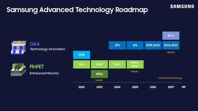
Samsung this week has unveiled its latest process technologies roadmap at the company's Samsung Foundry Forum (SFF) U.S. The new plan covers the evolution of Samsung's 2nm-class production nodes through 2027, including a process technology with a backside power delivery, re-emphasizing plans to bring out a 1.4nm-class node in 2027, and the introduction of a 'high value' 4nm-class manufacturing tech.
Samsung Foundry's key announcements for today are clearly focused on the its 2nm-class process technologies, which are set to enter production in 2025 and will span to 2027, when the company's 1.4-nm class production node is set to enter the scene. Samsung is also adding (or rather, renaming) another 2nm-class node to their roadmap with SF2, which was previously disclosed by Samsung as SF3P and aimed at high-performance devices.
"We have refined and improved the SF3P, resulting in what we now refer to as SF2," a Samsung spokesperson told AnandTech. "This enhanced node incorporates various process design improvements, delivering notable power, performance, and area (PPA) benefits."
| Samsung Foundry for Leading-Edge Nodes Announced on June 12, 2024 Compiled by AnandTech |
||||||||
| HVM Start | 2023 | 2024 | 2025 | 2026 | 2027 | 2027 | ||
| Process | SF3E | SF3 | SF2 (aka SF3P) |
SF2P/SF2X | SF2Z | SF1.4 | ||
| FET | GAAFET | |||||||
| Power Delivery | Frontside | Backside (BSPDN) | ? | |||||
| EUV | 0.33 NA EUV | ? | ? | ? | ? | |||
This is another example of a rebranding of leading-edge fabrication nodes in the recent years by a major chipmaker. Samsung Foundry is not disclosing any specific PPA improvements SF3P has over SF2, and for now is only stating in high-level terms that it will be a better-performing node than the planned SF3P.
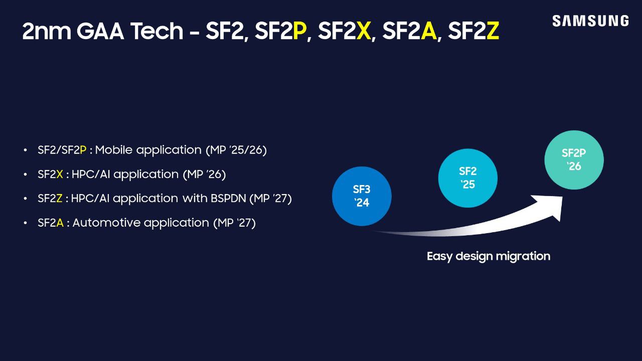
Meanwhile, this week's announcement also includes new information on Samsung's next batch of process nodes, which are planned for 2026 and 2027. In 2026 Samsung will have SF2P, a further refinement of SF2 which incorporates 'faster' yet less dense transistors. That will be followed up in 2027 with SF2Z, which adds backside power delivery to the mix for better and higher quality power delivery. In particular, Samsung is targetting voltate drop (aka IR drop) here, which is an ongoing concern in chip design.
Finally, SF1.4, a 1.4nm-class node, is on track for 2027 as well. Interestingly, however, it looks like it does not feature a backside power delivery. Which, per current roadmaps, would have Samsung as the only foundry not using BSPDN for their first 1.4nm/14Å-class node.
"We have optimized BSPDN and incorporated it for the first time in the SF2Z node we announced today," the spokesperso... Semiconductors

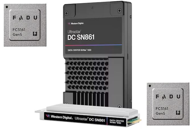
When Western Digital introduced its Ultrastar DC SN861 SSDs earlier this year, the company did not disclose which controller it used for these drives, which made many observers presume that WD was using an in-house controller. But a recent teardown of the drive shows that is not the case; instead, the company is using a controller from Fadu, a South Korean company founded in 2015 that specializes on enterprise-grade turnkey SSD solutions.
The Western Digital Ultrastar DC SN861 SSD is aimed at performance-hungry hyperscale datacenters and enterprise customers which are adopting PCIe Gen5 storage devices these days. And, as uncovered in photos from a recent Storage Review article, the drive is based on Fadu's FC5161 NVMe 2.0-compliant controller. The FC5161 utilizes 16 NAND channels supporting an ONFi 5.0 2400 MT/s interface, and features a combination of enterprise-grade capabilities (OCP Cloud Spec 2.0, SR-IOV, up to 512 name spaces for ZNS support, flexible data placement, NVMe-MI 1.2, advanced security, telemetry, power loss protection) not available on other off-the-shelf controllers – or on any previous Western Digital controllers.
The Ultrastar DC SN861 SSD offers sequential read speeds up to 13.7 GB/s as well as sequential write speeds up to 7.5 GB/s. As for random performance, it boasts with an up to 3.3 million random 4K read IOPS and up to 0.8 million random 4K write IOPS. The drives are available in capacities between 1.6 TB and 7.68 TB with one or three drive writes per day (DWPD) over five years rating as well as in U.2 and E1.S form-factors.
While the two form factors of the SN861 share a similar technical design, Western Digital has tailored each version for distinct workloads: the E1.S supports FDP and performance enhancements specifically for cloud environments. By contrast, the U.2 model is geared towards high-performance enterprise tasks and emerging applications like AI.
Without any doubts, Western Digital's Ultrastar DC SN861 is a feature-rich high-performance enterprise-grade SSD. It has another distinctive feature: a 5W idle power consumption, which is rather low by the standards of enterprise-grade drives (e.g., it is 1W lower compared to the SN840). While the difference with predecessors may be just 1W, hyperscalers deploy thousands of drives and for their TCO every watt counts.
Western Digital's Ultrastar DC SN861 SSDs are now available for purchase to select customers (such as Meta) and to interested parties. Prices are unknown, but they will depend on such factors as volumes.
Sources: Fadu, Storage Review
Storage
Samsung this week has unveiled its latest process technologies roadmap at the company's Samsung Foundry Forum (SFF) U.S. The new plan covers the evolution of Samsung's 2nm-class production nodes through 2027, including a process technology with a backside power delivery, re-emphasizing plans to bring out a 1.4nm-class node in 2027, and the introduction of a 'high value' 4nm-class manufacturing tech.
Samsung Foundry's key announcements for today are clearly focused on the its 2nm-class process technologies, which are set to enter production in 2025 and will span to 2027, when the company's 1.4-nm class production node is set to enter the scene. Samsung is also adding (or rather, renaming) another 2nm-class node to their roadmap with SF2, which was previously disclosed by Samsung as SF3P and aimed at high-performance devices.
"We have refined and improved the SF3P, resulting in what we now refer to as SF2," a Samsung spokesperson told AnandTech. "This enhanced node incorporates various process design improvements, delivering notable power, performance, and area (PPA) benefits."
| Samsung Foundry for Leading-Edge Nodes Announced on June 12, 2024 Compiled by AnandTech |
||||||||
| HVM Start | 2023 | 2024 | 2025 | 2026 | 2027 | 2027 | ||
| Process | SF3E | SF3 | SF2 (aka SF3P) |
SF2P/SF2X | SF2Z | SF1.4 | ||
| FET | GAAFET | |||||||
| Power Delivery | Frontside | Backside (BSPDN) | ? | |||||
| EUV | 0.33 NA EUV | ? | ? | ? | ? | |||
This is another example of a rebranding of leading-edge fabrication nodes in the recent years by a major chipmaker. Samsung Foundry is not disclosing any specific PPA improvements SF3P has over SF2, and for now is only stating in high-level terms that it will be a better-performing node than the planned SF3P.
Meanwhile, this week's announcement also includes new information on Samsung's next batch of process nodes, which are planned for 2026 and 2027. In 2026 Samsung will have SF2P, a further refinement of SF2 which incorporates 'faster' yet less dense transistors. That will be followed up in 2027 with SF2Z, which adds backside power delivery to the mix for better and higher quality power delivery. In particular, Samsung is targetting voltate drop (aka IR drop) here, which is an ongoing concern in chip design.
Finally, SF1.4, a 1.4nm-class node, is on track for 2027 as well. Interestingly, however, it looks like it does not feature a backside power delivery. Which, per current roadmaps, would have Samsung as the only foundry not using BSPDN for their first 1.4nm/14Å-class node.
"We have optimized BSPDN and incorporated it for the first time in the SF2Z node we announced today," the spokesperso... Semiconductors
When Western Digital introduced its Ultrastar DC SN861 SSDs earlier this year, the company did not disclose which controller it used for these drives, which made many observers presume that WD was using an in-house controller. But a recent teardown of the drive shows that is not the case; instead, the company is using a controller from Fadu, a South Korean company founded in 2015 that specializes on enterprise-grade turnkey SSD solutions.
The Western Digital Ultrastar DC SN861 SSD is aimed at performance-hungry hyperscale datacenters and enterprise customers which are adopting PCIe Gen5 storage devices these days. And, as uncovered in photos from a recent Storage Review article, the drive is based on Fadu's FC5161 NVMe 2.0-compliant controller. The FC5161 utilizes 16 NAND channels supporting an ONFi 5.0 2400 MT/s interface, and features a combination of enterprise-grade capabilities (OCP Cloud Spec 2.0, SR-IOV, up to 512 name spaces for ZNS support, flexible data placement, NVMe-MI 1.2, advanced security, telemetry, power loss protection) not available on other off-the-shelf controllers – or on any previous Western Digital controllers.
The Ultrastar DC SN861 SSD offers sequential read speeds up to 13.7 GB/s as well as sequential write speeds up to 7.5 GB/s. As for random performance, it boasts with an up to 3.3 million random 4K read IOPS and up to 0.8 million random 4K write IOPS. The drives are available in capacities between 1.6 TB and 7.68 TB with one or three drive writes per day (DWPD) over five years rating as well as in U.2 and E1.S form-factors.
While the two form factors of the SN861 share a similar technical design, Western Digital has tailored each version for distinct workloads: the E1.S supports FDP and performance enhancements specifically for cloud environments. By contrast, the U.2 model is geared towards high-performance enterprise tasks and emerging applications like AI.
Without any doubts, Western Digital's Ultrastar DC SN861 is a feature-rich high-performance enterprise-grade SSD. It has another distinctive feature: a 5W idle power consumption, which is rather low by the standards of enterprise-grade drives (e.g., it is 1W lower compared to the SN840). While the difference with predecessors may be just 1W, hyperscalers deploy thousands of drives and for their TCO every watt counts.
Western Digital's Ultrastar DC SN861 SSDs are now available for purchase to select customers (such as Meta) and to interested parties. Prices are unknown, but they will depend on such factors as volumes.
Sources: Fadu, Storage Review
Storage
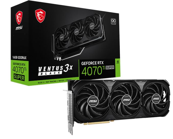
As GPU families enter the later part of their lifecycles, we often see chip manufacturers start to offload stockpiles of salvaged chips that, for one reason or another, didn't make the grade for the tier of cards they normally are used in. These recovered chips are fairly unremarkable overall, but they are unsold silicon that still works and has economic value, leading to them being used in lower-tier cards so that they can be sold. And, judging by the appearance of a new video card design from MSI, it looks like NVIDIA's Ada Lovelace generation of chips has reached that stage, as the Taiwanese video card maker has put out a new GeForce RTX 4070 Ti Super card based on a salvaged AD102 GPU.
Typically based on NVIDIA's AD103 GPU, NVIDIA's GeForce RTX 4070 Ti Super series sits a step below the company's flagship RTX 4080/4090 cards, both of which are based on the bigger and badder AD102 chip. But with some number of AD102 chips inevitably failing to live up to RTX 4080 specifications, rather than being thrown out, these chips can instead be used to make RTX 4070 cards. Which is exactly what MSI has done with their new GeForce RTX 4070 Ti Super Ventus 3X Black OC graphics card.
The card itself is relatively unremarkable – using a binned AD102 chip doesn't come with any advantages, and it should perform just like regular AD103 cards – and for that reason, video card vendors rarely publicly note when they're doing a run of cards with a binned-down version of a bigger chip. However, these larger chips have a tell-tale PCB footprint that usually makes it obvious what's going on. Which, as first noticed by @wxnod, is exactly what's going on with MSI's card.

Ada Lovelace Lineup: MSI GeForce RTX 4070 TiS (AD103), RTX 4070 TiS (AD102), & RTX 4090 (AD102)
The tell, in this case, is the rear board shot provided by MSI. The larger AD102 GPU uses an equally larger mounting bracket, and is paired with a slightly more complex array of filtering capacitors on the back side of the board PCB. Ultimately, since these are visible in MSI's photos of their GeForce RTX 4070 Ti Super Ventus 3X Black OC, it's easy to compare it to other video cards and see that it has exactly the same capacitor layout as MSI's GeForce RTX 4090, thus confirming the use of an AD102 GPU.
Chip curiosities aside, all of NVIDIA GeForce RTX 4070 Ti Super graphics cards – no matter whether they are based on the AD102 or AD103 GPU – come with a GPU with 8,448 active CUDA cores and 16 GB of GDDR6X memory, so it doesn't (typically) matter which chip they carry. Otherwise, compared to a fully-enabled AD102 chip, the RTX 4070 Ti Super specifications are relatively modest, with fewer than half as many CUDA cores, underscoring how the AD102 chip being used in MSI's card is a pretty heavy salvage bin.
As for the rest of the card, MSI GeForce RTX 4070 Ti Super Ventus 3X Black OC is a relatively hefty card overall, with a cooling system to match. Being overclocked, the Ventus also has a slightly higher TDP than normal GeForce RTX 4070 Ti Super cards, weighing in at 295 Watts, or 10 Watts above baseline cards.
Meanwhile, MSI is apparently not the only video card manufacturer using salvaged AD102 chips for GeForce RTX 4070 Ti Super, either. @wxnod has also posted a screenshot obtained on an Inno3D GeForce RTX 4070 Ti Super based on an AD102 GPU.
GPUs
Lorem Ipsum is simply dummy text of the printing and typesetting industry. Lorem Ipsum has been the industry's.
Samsung this week has unveiled its latest process technologies roadmap at the company's Samsung Foundry Forum (SFF) U.S. The new plan covers the evolution of Samsung's 2nm-class production nodes through 2027, including a process technology with a backside power delivery, re-emphasizing plans to bring out a 1.4nm-class node in 2027, and the introduction of a 'high value' 4nm-class manufacturing tech.
Samsung Foundry's key announcements for today are clearly focused on the its 2nm-class process technologies, which are set to enter production in 2025 and will span to 2027, when the company's 1.4-nm class production node is set to enter the scene. Samsung is also adding (or rather, renaming) another 2nm-class node to their roadmap with SF2, which was previously disclosed by Samsung as SF3P and aimed at high-performance devices.
"We have refined and improved the SF3P, resulting in what we now refer to as SF2," a Samsung spokesperson told AnandTech. "This enhanced node incorporates various process design improvements, delivering notable power, performance, and area (PPA) benefits."
| Samsung Foundry for Leading-Edge Nodes Announced on June 12, 2024 Compiled by AnandTech |
||||||||
| HVM Start | 2023 | 2024 | 2025 | 2026 | 2027 | 2027 | ||
| Process | SF3E | SF3 | SF2 (aka SF3P) |
SF2P/SF2X | SF2Z | SF1.4 | ||
| FET | GAAFET | |||||||
| Power Delivery | Frontside | Backside (BSPDN) | ? | |||||
| EUV | 0.33 NA EUV | ? | ? | ? | ? | |||
This is another example of a rebranding of leading-edge fabrication nodes in the recent years by a major chipmaker. Samsung Foundry is not disclosing any specific PPA improvements SF3P has over SF2, and for now is only stating in high-level terms that it will be a better-performing node than the planned SF3P.
Meanwhile, this week's announcement also includes new information on Samsung's next batch of process nodes, which are planned for 2026 and 2027. In 2026 Samsung will have SF2P, a further refinement of SF2 which incorporates 'faster' yet less dense transistors. That will be followed up in 2027 with SF2Z, which adds backside power delivery to the mix for better and higher quality power delivery. In particular, Samsung is targetting voltate drop (aka IR drop) here, which is an ongoing concern in chip design.
Finally, SF1.4, a 1.4nm-class node, is on track for 2027 as well. Interestingly, however, it looks like it does not feature a backside power delivery. Which, per current roadmaps, would have Samsung as the only foundry not using BSPDN for their first 1.4nm/14Å-class node.
"We have optimized BSPDN and incorporated it for the first time in the SF2Z node we announced today," the spokesperso... Semiconductors
When Western Digital introduced its Ultrastar DC SN861 SSDs earlier this year, the company did not disclose which controller it used for these drives, which made many observers presume that WD was using an in-house controller. But a recent teardown of the drive shows that is not the case; instead, the company is using a controller from Fadu, a South Korean company founded in 2015 that specializes on enterprise-grade turnkey SSD solutions.
The Western Digital Ultrastar DC SN861 SSD is aimed at performance-hungry hyperscale datacenters and enterprise customers which are adopting PCIe Gen5 storage devices these days. And, as uncovered in photos from a recent Storage Review article, the drive is based on Fadu's FC5161 NVMe 2.0-compliant controller. The FC5161 utilizes 16 NAND channels supporting an ONFi 5.0 2400 MT/s interface, and features a combination of enterprise-grade capabilities (OCP Cloud Spec 2.0, SR-IOV, up to 512 name spaces for ZNS support, flexible data placement, NVMe-MI 1.2, advanced security, telemetry, power loss protection) not available on other off-the-shelf controllers – or on any previous Western Digital controllers.
The Ultrastar DC SN861 SSD offers sequential read speeds up to 13.7 GB/s as well as sequential write speeds up to 7.5 GB/s. As for random performance, it boasts with an up to 3.3 million random 4K read IOPS and up to 0.8 million random 4K write IOPS. The drives are available in capacities between 1.6 TB and 7.68 TB with one or three drive writes per day (DWPD) over five years rating as well as in U.2 and E1.S form-factors.
While the two form factors of the SN861 share a similar technical design, Western Digital has tailored each version for distinct workloads: the E1.S supports FDP and performance enhancements specifically for cloud environments. By contrast, the U.2 model is geared towards high-performance enterprise tasks and emerging applications like AI.
Without any doubts, Western Digital's Ultrastar DC SN861 is a feature-rich high-performance enterprise-grade SSD. It has another distinctive feature: a 5W idle power consumption, which is rather low by the standards of enterprise-grade drives (e.g., it is 1W lower compared to the SN840). While the difference with predecessors may be just 1W, hyperscalers deploy thousands of drives and for their TCO every watt counts.
Western Digital's Ultrastar DC SN861 SSDs are now available for purchase to select customers (such as Meta) and to interested parties. Prices are unknown, but they will depend on such factors as volumes.
Sources: Fadu, Storage Review
Storage

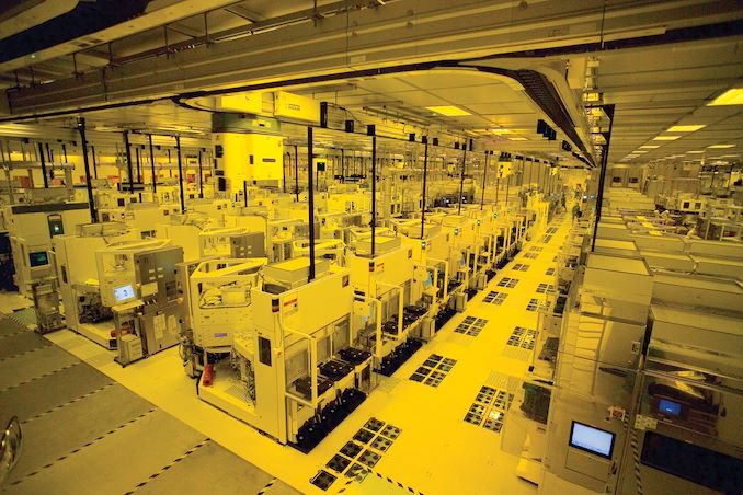
![TSMC to Expand Specialty Capacity by 50%, Introduce 4nm N4e Low-Power Node <p align="center"><a href="https://www.anandtech.com/show/21397/tsmc-to-expand-specialty-capacity-by-50-introduce-4nm-lowpower-node"><img src="https://images.anandtech.com/doci/21397/tsmc-semiconductor-fab-wafer-1-678_575px.jpg" alt="" /></a></p><p><p>With all the new fabs being built in Germany and Japan, as well as the expansion of production capacity in China, TSMC is planning to extend its production capacity for specialty technologies by 50% by 2027. As disclosed by the company during its European Technology Symposium this week, TSMC expects to need to not only convert existing capacity to meet demands for specialty processes, but even build new (greenfield) fab space just for this purpose. One of the big drivers for this demand, in turn, will be TSMC's next specialty node: N4e, a 4nm-class ultra-low-power production node.</p>
<p>"In the past, we always did the review phase [for upcoming fabs], but for the first time in a long time at TSMC, we started building greenfield fab that will address the future specialty technology requirements," said Dr. Kevin Zhang, Senior Vice President, Business Development and Overseas Operations Office, at the event. "In the next four to five years, we actually going to grow our specialty capacity by up to 1.5x. In doing so we actually expanding the footprint of our manufacturing network to improve the resiliency of the overall fab supply chain."</p>
<p>On top of its well-known major logic nodes like N5 and N3E, TSMC also offers a suite of specialty nodes for applications such as power semiconductors, mixed analog I/O, and ultra-low-power applications (e.g. IoT). These are typically based on the company's trailing manufacturing processes, but regardless of the underlying technology, the capacity demand for these nodes is growing right alongside the demand for TSMC's major logic nodes. All of which has required TSMC to reevaluate how they go about planning for capacity on their specialty nodes.</p>
<p>TSMC's expansion strategy in the recent years has pursued several goals. One of them has been to build new fabs outside of Taiwan; another has been to generally expand production capacity to meet future demand for all types of process technologies – which is why the company is building up capacity for specialty nodes.</p>
<p>At present, TSMC's most advanced specialty node is N6e, an N7/N6 variant that supports operating voltages between 0.4V and 0.9V. With N4e, TSMC is looking at voltages below 0.4V. Though for now, TSMC is not disclosing much in the way of technical details for the planned node; given the company's history here, we expect they'll have more to talk about next year once the new process is ready.</p>
</p> Semiconductors](https://lh3.googleusercontent.com/blogger_img_proxy/AEn0k_uhAMZMX1awzZkMNFQpazmJESWWbRLVvJq5xoSwov-e-6y_sTSLSY03hpIjHDkAJL_c6HsPULHKHF829veAd1DX9W8tkZBcdaQi_V7sBUvnm_QZSFdmcDnyQvksbGyrWjZURXSMDFvi72lgdEbm3LceRVOlNvK-JQ=w72-h72-p-k-no-nu)
. The chips are accompanied by various other components, such as power management ICs, but in general it relies solely on in-house developed components, which is why it can be made so cheap. </p>
<p style="text-align: center;"><a href="https://www.anandtech.com/show/21449/realtek-has-a-platform-for-sub100-5gbe-switch"><img alt="" src="https://images.anandtech.com/doci/21449/IMG_0075-phy_575px.jpg" /></a></p>
<p>RealTek's platform is meant for home and small offices, which is reflected in the switch's feature set. This is a simple, unmanaged switch with a handful of ports, making it ideal for linking up a few systems, while enterprise users will likely find it a bit too basic.</p>
<p>Segmenting the market like this is ultimately critical for bringing down the price of hardware. The bulk of 5GbE/10GbE switches on the market today are more enterprise-focused managed switches, which carry more features and a price premium to match. So developing a stripped-down platform for cheaper consumer switches is a huge development that should finally make it economical for consumers to adopt faster networking hardware, similar to 2.5GbE a few years ago.</p>
<p>At present, 2.5GbE switches are running at around $20/port, so RealTek's sub-$100 target for a 4-port switch aims to bring 5GbE in at just a slightly higher price tag of $25/port. Or, compared to the handful of unmanaged 10GbE switches on the market, which average $60/port, this will be less than half the price (though at half the bandwidth).</p>
<p>The proliferation of cheap 5GbE network switches will also mark a notable inflection point in Ethernet hardware design, as it's the fastest standard that is rated to work the ubiquitous Cat 5e cable. The NBASE-T standard was penned almost a decade ago in order to cover the missing-middle between 1GbE and 10GbE, while getting more bandwidth out of existing, widely-deployed Cat 5e cabling. So with the release of consumer 5GbE gear, the standard's goals are finally coming to fruition – though it does mean we're finally reaching the end of the road for the oldest network cabling still widely in use.</p>
<p style="text-align: center;"><a href="https://www.anandtech.com/show/21449/realtek-has-a-platform-for-sub100-5gbe-switch"><img alt="" src="https://images.anandtech.com/doci/21449/IMG_0074-realtek-chip_575px.jpg" /></a></p>
<p>For now, Realtek is only talking about one customer offering a sub-$100 5GbE switch this September, but something tells me that other partners of the company will come up with similar devices soon enough. As a result of the competition, prices could get even lower, which is always good for buyers.</p>
<p>These benefits should also funnel into Wi-Fi 7 routers, to a limited extent. Wired backhaul speeds need to keep pace with ever-faster Wi-Fi standards in order to keep those newer radios fed, so it's not a coincidence that cheaper 5GbE is finally coming right as Wi-Fi 7 is taking off.</p>
<p>Overall, the company's 5GbE switch platform is part of a larger ecosystem of 5GbE hardware that Realtek was showing off at Computex. In addition to RTL8251B 5GbE PHYs and RTL9303 switch SoC, the company is also preparing their RTL8126 PCIe 3.1 network controller, and RTL8157 NIC for USB dongles.</p>
</p> Networking)
. The chips are accompanied by various other components, such as power management ICs, but in general it relies solely on in-house developed components, which is why it can be made so cheap. </p>
<p style="text-align: center;"><a href="https://www.anandtech.com/show/21449/realtek-has-a-platform-for-sub100-5gbe-switch"><img alt="" src="https://images.anandtech.com/doci/21449/IMG_0075-phy_575px.jpg" /></a></p>
<p>RealTek's platform is meant for home and small offices, which is reflected in the switch's feature set. This is a simple, unmanaged switch with a handful of ports, making it ideal for linking up a few systems, while enterprise users will likely find it a bit too basic.</p>
<p>Segmenting the market like this is ultimately critical for bringing down the price of hardware. The bulk of 5GbE/10GbE switches on the market today are more enterprise-focused managed switches, which carry more features and a price premium to match. So developing a stripped-down platform for cheaper consumer switches is a huge development that should finally make it economical for consumers to adopt faster networking hardware, similar to 2.5GbE a few years ago.</p>
<p>At present, 2.5GbE switches are running at around $20/port, so RealTek's sub-$100 target for a 4-port switch aims to bring 5GbE in at just a slightly higher price tag of $25/port. Or, compared to the handful of unmanaged 10GbE switches on the market, which average $60/port, this will be less than half the price (though at half the bandwidth).</p>
<p>The proliferation of cheap 5GbE network switches will also mark a notable inflection point in Ethernet hardware design, as it's the fastest standard that is rated to work the ubiquitous Cat 5e cable. The NBASE-T standard was penned almost a decade ago in order to cover the missing-middle between 1GbE and 10GbE, while getting more bandwidth out of existing, widely-deployed Cat 5e cabling. So with the release of consumer 5GbE gear, the standard's goals are finally coming to fruition – though it does mean we're finally reaching the end of the road for the oldest network cabling still widely in use.</p>
<p style="text-align: center;"><a href="https://www.anandtech.com/show/21449/realtek-has-a-platform-for-sub100-5gbe-switch"><img alt="" src="https://images.anandtech.com/doci/21449/IMG_0074-realtek-chip_575px.jpg" /></a></p>
<p>For now, Realtek is only talking about one customer offering a sub-$100 5GbE switch this September, but something tells me that other partners of the company will come up with similar devices soon enough. As a result of the competition, prices could get even lower, which is always good for buyers.</p>
<p>These benefits should also funnel into Wi-Fi 7 routers, to a limited extent. Wired backhaul speeds need to keep pace with ever-faster Wi-Fi standards in order to keep those newer radios fed, so it's not a coincidence that cheaper 5GbE is finally coming right as Wi-Fi 7 is taking off.</p>
<p>Overall, the company's 5GbE switch platform is part of a larger ecosystem of 5GbE hardware that Realtek was showing off at Computex. In addition to RTL8251B 5GbE PHYs and RTL9303 switch SoC, the company is also preparing their RTL8126 PCIe 3.1 network controller, and RTL8157 NIC for USB dongles.</p>
</p> Networking)
. The chips are accompanied by various other components, such as power management ICs, but in general it relies solely on in-house developed components, which is why it can be made so cheap. </p>
<p style="text-align: center;"><a href="https://www.anandtech.com/show/21449/realtek-has-a-platform-for-sub100-5gbe-switch"><img alt="" src="https://images.anandtech.com/doci/21449/IMG_0075-phy_575px.jpg" /></a></p>
<p>RealTek's platform is meant for home and small offices, which is reflected in the switch's feature set. This is a simple, unmanaged switch with a handful of ports, making it ideal for linking up a few systems, while enterprise users will likely find it a bit too basic.</p>
<p>Segmenting the market like this is ultimately critical for bringing down the price of hardware. The bulk of 5GbE/10GbE switches on the market today are more enterprise-focused managed switches, which carry more features and a price premium to match. So developing a stripped-down platform for cheaper consumer switches is a huge development that should finally make it economical for consumers to adopt faster networking hardware, similar to 2.5GbE a few years ago.</p>
<p>At present, 2.5GbE switches are running at around $20/port, so RealTek's sub-$100 target for a 4-port switch aims to bring 5GbE in at just a slightly higher price tag of $25/port. Or, compared to the handful of unmanaged 10GbE switches on the market, which average $60/port, this will be less than half the price (though at half the bandwidth).</p>
<p>The proliferation of cheap 5GbE network switches will also mark a notable inflection point in Ethernet hardware design, as it's the fastest standard that is rated to work the ubiquitous Cat 5e cable. The NBASE-T standard was penned almost a decade ago in order to cover the missing-middle between 1GbE and 10GbE, while getting more bandwidth out of existing, widely-deployed Cat 5e cabling. So with the release of consumer 5GbE gear, the standard's goals are finally coming to fruition – though it does mean we're finally reaching the end of the road for the oldest network cabling still widely in use.</p>
<p style="text-align: center;"><a href="https://www.anandtech.com/show/21449/realtek-has-a-platform-for-sub100-5gbe-switch"><img alt="" src="https://images.anandtech.com/doci/21449/IMG_0074-realtek-chip_575px.jpg" /></a></p>
<p>For now, Realtek is only talking about one customer offering a sub-$100 5GbE switch this September, but something tells me that other partners of the company will come up with similar devices soon enough. As a result of the competition, prices could get even lower, which is always good for buyers.</p>
<p>These benefits should also funnel into Wi-Fi 7 routers, to a limited extent. Wired backhaul speeds need to keep pace with ever-faster Wi-Fi standards in order to keep those newer radios fed, so it's not a coincidence that cheaper 5GbE is finally coming right as Wi-Fi 7 is taking off.</p>
<p>Overall, the company's 5GbE switch platform is part of a larger ecosystem of 5GbE hardware that Realtek was showing off at Computex. In addition to RTL8251B 5GbE PHYs and RTL9303 switch SoC, the company is also preparing their RTL8126 PCIe 3.1 network controller, and RTL8157 NIC for USB dongles.</p>
</p> Networking | https://compbuddey.blogspot.com/2024/07/realtek-previews-platform-for-sub-100_2.html)
. The chips are accompanied by various other components, such as power management ICs, but in general it relies solely on in-house developed components, which is why it can be made so cheap. </p>
<p style="text-align: center;"><a href="https://www.anandtech.com/show/21449/realtek-has-a-platform-for-sub100-5gbe-switch"><img alt="" src="https://images.anandtech.com/doci/21449/IMG_0075-phy_575px.jpg" /></a></p>
<p>RealTek's platform is meant for home and small offices, which is reflected in the switch's feature set. This is a simple, unmanaged switch with a handful of ports, making it ideal for linking up a few systems, while enterprise users will likely find it a bit too basic.</p>
<p>Segmenting the market like this is ultimately critical for bringing down the price of hardware. The bulk of 5GbE/10GbE switches on the market today are more enterprise-focused managed switches, which carry more features and a price premium to match. So developing a stripped-down platform for cheaper consumer switches is a huge development that should finally make it economical for consumers to adopt faster networking hardware, similar to 2.5GbE a few years ago.</p>
<p>At present, 2.5GbE switches are running at around $20/port, so RealTek's sub-$100 target for a 4-port switch aims to bring 5GbE in at just a slightly higher price tag of $25/port. Or, compared to the handful of unmanaged 10GbE switches on the market, which average $60/port, this will be less than half the price (though at half the bandwidth).</p>
<p>The proliferation of cheap 5GbE network switches will also mark a notable inflection point in Ethernet hardware design, as it's the fastest standard that is rated to work the ubiquitous Cat 5e cable. The NBASE-T standard was penned almost a decade ago in order to cover the missing-middle between 1GbE and 10GbE, while getting more bandwidth out of existing, widely-deployed Cat 5e cabling. So with the release of consumer 5GbE gear, the standard's goals are finally coming to fruition – though it does mean we're finally reaching the end of the road for the oldest network cabling still widely in use.</p>
<p style="text-align: center;"><a href="https://www.anandtech.com/show/21449/realtek-has-a-platform-for-sub100-5gbe-switch"><img alt="" src="https://images.anandtech.com/doci/21449/IMG_0074-realtek-chip_575px.jpg" /></a></p>
<p>For now, Realtek is only talking about one customer offering a sub-$100 5GbE switch this September, but something tells me that other partners of the company will come up with similar devices soon enough. As a result of the competition, prices could get even lower, which is always good for buyers.</p>
<p>These benefits should also funnel into Wi-Fi 7 routers, to a limited extent. Wired backhaul speeds need to keep pace with ever-faster Wi-Fi standards in order to keep those newer radios fed, so it's not a coincidence that cheaper 5GbE is finally coming right as Wi-Fi 7 is taking off.</p>
<p>Overall, the company's 5GbE switch platform is part of a larger ecosystem of 5GbE hardware that Realtek was showing off at Computex. In addition to RTL8251B 5GbE PHYs and RTL9303 switch SoC, the company is also preparing their RTL8126 PCIe 3.1 network controller, and RTL8157 NIC for USB dongles.</p>
</p> Networking&body=https://compbuddey.blogspot.com/2024/07/realtek-previews-platform-for-sub-100_2.html)


0 Comments