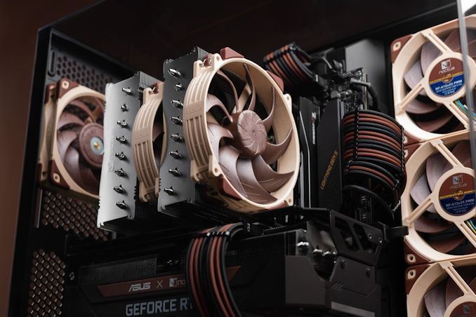

On Tuesday, Noctua introduced its second-generation NH-D15 cooler, which offers refined performance and formally supports Intel's next-generation Arrow Lake-S processors in LGA1851 packaging. Alongside its NH-D15 G2 CPU cooler, Noctua also introduced its NF-A14x25r G2 140mm fans.
The Noctua NH-D15 G2 is an enhanced version of the popular NH-D15 cooler with eight heat pipes, two asymmetrical fin-stack and two speed-offset 140-mm PWM fans (to avoid acoustic interaction phenomena such as periodic humming or intermittent vibrations). According to the manufacturer, these key components are tailored to work efficiently together to deliver superior quiet cooling performance, rivalling many all-in-one water cooling systems and pushing the boundaries of air cooling efficiency.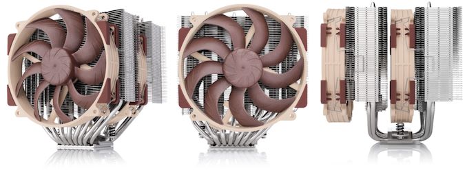
Noctua offers the NH-D15 G2 in three versions to address the specific requirements of modern CPUs. The regular version is versatile and can be used for AMD's AM5 processors and Intel's LGA1700 CPUs with included mounting accessories. The HBC (High Base Convexity) variant is tailored for LGA1700 processors, especially those subjected to full ILM pressure or those that have deformed over time, ensuring excellent contact quality despite the concave shape of the CPU. Finally, the LBC (Low Base Convexity) version is tailored for flat rectangular CPUs, providing optimal contact on AMD's AM5 and other similar processors.
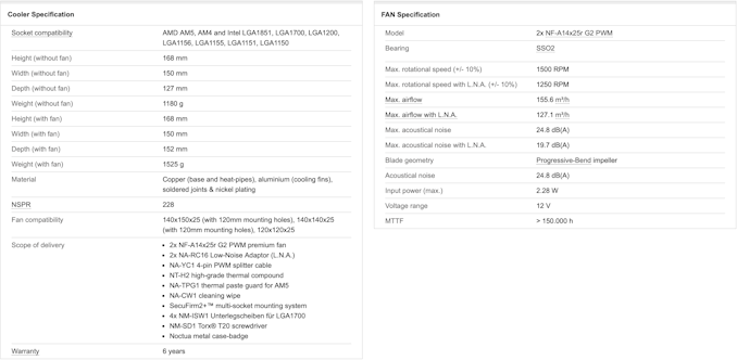
While there are three versions of NH-D15 G2 aimed at different processors, they are all said to be compatible with a wide range of motherboards and other hardware. The new coolers' offset construction ensures clearance for the top PCIe x16 slot on most current motherboards. Additionally, they feature the upgraded Torx-based SecuFirm2+ multi-socket mounting system and come with Noctua's NT-H2 thermal compound.
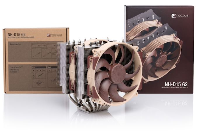
For those looking to upgrade existing coolers like the NH-D15, NH-D15S, or NH-U14S series, Noctua is also releasing the NF-A14x25r G2 fans separately. These round-frame fans are fine-tuned in single and dual fan packages to minimize noise levels while offering decent cooling performance.
Finally, Noctua is also prepping a square-frame version of the NF-A14x25 G2 fan for release in September. This variant targets water-cooling radiators and case-cooling applications and promises to extend the versatility of Noctua's cooling solutions further.
All versions of Noctua's NH-D15 G2 coolers cost $149.90/€149.90. One NF-A14x25 G2 fan costs $39.90/€39.90, whereas a package of two fans costs $79.80/€79.80. The cooler is backed with a six-year warranty.
Cases/Cooling/PSUs

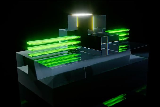
In addition to revealing its roadmap and plans concerning its current leading-edge process technologies, TSMC also shared progress of its N2 node as part of its Symposiums 2024. The company's first 2nm-class fabrication node, and predominantly featuring gate-all-around transistors, according to TSMC N2 has almost achieved its target performance and yield goals, which places it on track to enter high-volume manufacturing in the second half of 2025.
TSMC states that 'N2 development is well on track and N2P is next.' In particular, gate-all-around nanosheet devices currently achieve over 90% of their expected performance, whereas yields of 256 Mb SRAM (32 MB) devices already exceeds 80%, depending on the batch. All of this for a node that is over a year away from mass production.
Meanwhile, average yield of a 256 Mb SRAM was around 70% as of March, 2024, up from around 35% in April, 2023. Device performance has also been improving with higher frequencies being achieved while keeping power consumption in check.
Chip designer interest towards TSMC's first 2nm-class gate-all-around nanosheet transistor-based technology is significant, too. The number of new tape-outs (NTOs) in the first year of N2 is over two-times higher than it was for N5. Though with that said, given TSMC's close working relationship with a handful of high-volume vendors – most notably Appe – NTOs can be a very misleading figure since the first year of a new node at TSMC is capacity constrained, and consequently the bulk of that capacity goes to TSMC's priority partners.
Meanwhile, there were considerably more N5 tapeouts in its second year (some where N5P, of course) and N2 promises to have 2.6X more NTOs in its second year. So the node indeed looks quite promising. In fact, based on TSMC's slides (which we're unfortunately not able to republish), N2 is more popular than N3 in terms of NTOs both in the first and the second years of existence.
When it comes to the second year of N2, in the second half of 2026 TSMC plans to roll out its N2P technology, which promises additional performance and power benefits. N2P is expected to improve frequency by 15% - 20%, reduce power consumption by 30% - 40%, and increase chip density by over 1.15 times compared to N3E, significant benefits to move to all-new GAA nanosheet transistors.
Finally, for those companies that need the best in performance, power, and density, TSMC is poised to offer their A16 process in 2026. That node will also bring in backside power delivery, which will add costs, but is expected to greatly improve performance efficiency and scaling.
Semiconductors
In addition to revealing its roadmap and plans concerning its current leading-edge process technologies, TSMC also shared progress of its N2 node as part of its Symposiums 2024. The company's first 2nm-class fabrication node, and predominantly featuring gate-all-around transistors, according to TSMC N2 has almost achieved its target performance and yield goals, which places it on track to enter high-volume manufacturing in the second half of 2025.
TSMC states that 'N2 development is well on track and N2P is next.' In particular, gate-all-around nanosheet devices currently achieve over 90% of their expected performance, whereas yields of 256 Mb SRAM (32 MB) devices already exceeds 80%, depending on the batch. All of this for a node that is over a year away from mass production.
Meanwhile, average yield of a 256 Mb SRAM was around 70% as of March, 2024, up from around 35% in April, 2023. Device performance has also been improving with higher frequencies being achieved while keeping power consumption in check.
Chip designer interest towards TSMC's first 2nm-class gate-all-around nanosheet transistor-based technology is significant, too. The number of new tape-outs (NTOs) in the first year of N2 is over two-times higher than it was for N5. Though with that said, given TSMC's close working relationship with a handful of high-volume vendors – most notably Appe – NTOs can be a very misleading figure since the first year of a new node at TSMC is capacity constrained, and consequently the bulk of that capacity goes to TSMC's priority partners.
Meanwhile, there were considerably more N5 tapeouts in its second year (some where N5P, of course) and N2 promises to have 2.6X more NTOs in its second year. So the node indeed looks quite promising. In fact, based on TSMC's slides (which we're unfortunately not able to republish), N2 is more popular than N3 in terms of NTOs both in the first and the second years of existence.
When it comes to the second year of N2, in the second half of 2026 TSMC plans to roll out its N2P technology, which promises additional performance and power benefits. N2P is expected to improve frequency by 15% - 20%, reduce power consumption by 30% - 40%, and increase chip density by over 1.15 times compared to N3E, significant benefits to move to all-new GAA nanosheet transistors.
Finally, for those companies that need the best in performance, power, and density, TSMC is poised to offer their A16 process in 2026. That node will also bring in backside power delivery, which will add costs, but is expected to greatly improve performance efficiency and scaling.
Semiconductors
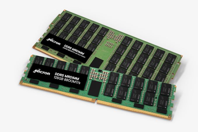
Following a relative lull in the desktop memory industry in the previous decade, the past few years have seen a flurry of new memory standards and form factors enter development. Joining the traditional DIMM/SO-DIMM form factors, we've seen the introduction of space-efficient DDR5 CAMM2s, their LPDDR5-based counterpart the LPCAMM2, and the high-clockspeed optimized CUDIMM. But JEDEC, the industry organization behind these efforts, is not done there. In a press release sent out at the start of the week, the group announced that it is working on standards for DDR5 Multiplexed Rank DIMMs (MRDIMM) for servers, as well as an updated LPCAMM standard to go with next-generation LPDDR6 memory.
Just last week Micron introduced the industry's first DDR5 MRDIMMs, which are timed to launch alongside Intel's Xeon 6 server platforms. But while Intel and its partners are moving full steam ahead on MRDIMMs, the MRDIMM specification has not been fully ratified by JEDEC itself. All told, it's not unusual to see Intel pushing the envelope here on new memory technologies (the company is big enough to bootstrap its own ecosystem). But as MRDIMMs are ultimately meant to be more than just a tool for Intel, a proper industry standard is still needed – even if that takes a bit longer.
Under the hood, MRDIMMs continue to use DDR5 components, form-factor, pinout, SPD, power management ICs (PMICs), and thermal sensors. The major change with the technology is the introduction of multiplexing, which combines multiple data signals over a single channel. The MRDIMM standard also adds RCD/DB logic in a bid to boost performance, increase capacity of memory modules up to 256 GB (for now), shrink latencies, and reduce power consumption of high-end memory subsystems. And, perhaps key to MRDIMM adoption, the standard is being implemented as a backwards-compatible extension to traditional DDR5 RDIMMs, meaning that MRDIMM-capable servers can use either RDIMMs or MRDIMMs, depending on how the operator opts to configure the system.
The MRDIMM standard aims to double the peak bandwidth to 12.8 Gbps, increasing pin speed and supporting more than two ranks. Additionally, a "Tall MRDIMM" form factor is in the works (and pictured above), which is designed to allow for higher capacity DIMMs by providing more area for laying down memory chips. Currently, ultra high capacity DIMMs require using expensive, multi-layer DRAM packages that use through-silicon vias (3DS packaging) to attach the individual DRAM dies; a Tall MRDIMM, on the other hand, can just use a larger number of commodity DRAM chips. Overall, the Tall MRDIMM form factor enables twice the number of DRAM single-die packages on the DIMM.
Meanwhile, this week's announcement from JEDEC offers the first significant insight into what to expect from LPDDR6 CAMMs. And despite LPDDR5 CAMMs having barely made it out the door, some significant shifts with LPDDR6 itself means that JEDEC will need to make some major changes to the CAMM standard to accommodate the newer memory type.
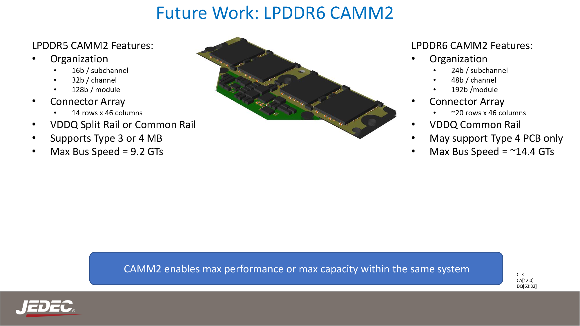
JEDEC Presentation: The CAMM2 Journey and Future Potential
Besides the higher memory clockspeeds allowed by LPDDR6 – JEDEC is targeting data transfer rates of 14.4 GT/s and higher – the new memory form-factor will also incorporate an altogether new connector array. This is to accommodate LPDDR6's wider memory bus, which sees the channel width of an individual memory chip grow from 16-bits wide to 24-bits wide. As a result, the current LPCAMM design, which is intended to match the PC standard of a cumulative 128-bit (16x8) design needs to be reconfigured to match LPDDR6's alterations.
Ultimately, JEDEC is targeting a 24-bit subhannel/48-bit channel design, which will result in a 192-bit wide LPCAMM. While the LPCAMM connector itself is set to grow from 14 rows of pins to possibly as high as 20. New memory technologies typically require new DIMMs to begin with, so it's important to clarify that this is not unexpected, but at th... Memory

As Qualcomm prepares for the mid-year launch of their forthcoming Snapdragon X SoCs for PCs, and the eagerly anticipated Oryon CPU cores within, the company is finally shoring up their official product plans, and releasing some additional technical details in the process. Thus far the company has been demonstrating their Snapdragon X Elite SoC in its highest-performing, fully-enabled configuration. But the retail Snapdragon X Elite will not be a single part; instead, Qualcomm is preparing a whole range of chip configurations for various price/performance tiers in the market. Altogether, there will be 3 Snapdragon X Elite SKUs that differ in CPU and GPU performance.
As well, the company is introducing a second Snapdragon X tier, Snapdragon X Plus, for those SKUs positioned below the Elite performance tier. As of today, this will be a single configuration. But if the Snapdragon X lineup is successful and demand warrants it, I would not be surprised to see Qualcomm expand it further – as they have certainly left themselves the room for it in their product stack. In the meantime, with Qualcomm’s expected launch competition now shipping (Intel Core Ultra Meteor Lake and AMD Ryzen Mobile 8040 Hawk Point), the company is also very confident that even these reduced performance Snapdragon X Plus chips will be able to beat Intel and AMD in multithreaded performance – never mind the top-tier Snapdragon X Elite chips.
Qualcomm will be launching this expanded four chip stack at once; so both Snapdragon X Elite and Snapdragon X Plus tier devices should be available at the same time. The company’s goal is still to have devices on the shelf “mid-year”, although the company isn’t providing any more precise guidance than that. With Qualcomm’s CEO, Cristiano Amon, set to deliver a Computex keynote in June, I expect we’ll get more specific details on timings then, along with the company and its partners using the event to announce and showcase some retail laptop designs. So this is very much looking like a summer launch at the moment.
In the meantime, Qualcomm is already showing off what their Snapdragon X Plus chips can do with a fresh set of live benchmarks, akin to their Snapdragon X Elite performance previews from October 2023. We’ll dive into those in a bit, but suffice it to say, Qualcomm knows the score, and they want to make sure the entire world knows when they’re winning.
CPUs
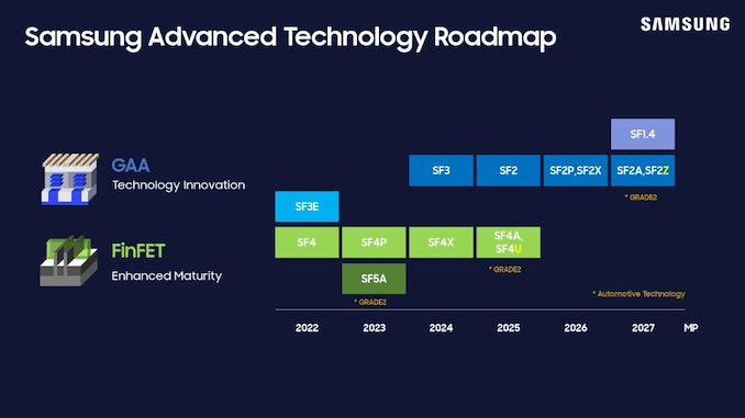
Samsung this week has unveiled its latest process technologies roadmap at the company's Samsung Foundry Forum (SFF) U.S. The new plan covers the evolution of Samsung's 2nm-class production nodes through 2027, including a process technology with a backside power delivery, re-emphasizing plans to bring out a 1.4nm-class node in 2027, and the introduction of a 'high value' 4nm-class manufacturing tech.
Samsung Foundry's key announcements for today are clearly focused on the its 2nm-class process technologies, which are set to enter production in 2025 and will span to 2027, when the company's 1.4-nm class production node is set to enter the scene. Samsung is also adding (or rather, renaming) another 2nm-class node to their roadmap with SF2, which was previously disclosed by Samsung as SF3P and aimed at high-performance devices.
"We have refined and improved the SF3P, resulting in what we now refer to as SF2," a Samsung spokesperson told AnandTech. "This enhanced node incorporates various process design improvements, delivering notable power, performance, and area (PPA) benefits."
| Samsung Foundry for Leading-Edge Nodes Announced on June 12, 2024 Compiled by AnandTech |
||||||||
| HVM Start | 2023 | 2024 | 2025 | 2026 | 2027 | 2027 | ||
| Process | SF3E | SF3 | SF2 (aka SF3P) |
SF2P/SF2X | SF2Z | SF1.4 | ||
| FET | GAAFET | |||||||
| Power Delivery | Frontside | Backside (BSPDN) | ? | |||||
| EUV | 0.33 NA EUV | ? | ? | ? | ? | |||
This is another example of a rebranding of leading-edge fabrication nodes in the recent years by a major chipmaker. Samsung Foundry is not disclosing any specific PPA improvements SF3P has over SF2, and for now is only stating in high-level terms that it will be a better-performing node than the planned SF3P.
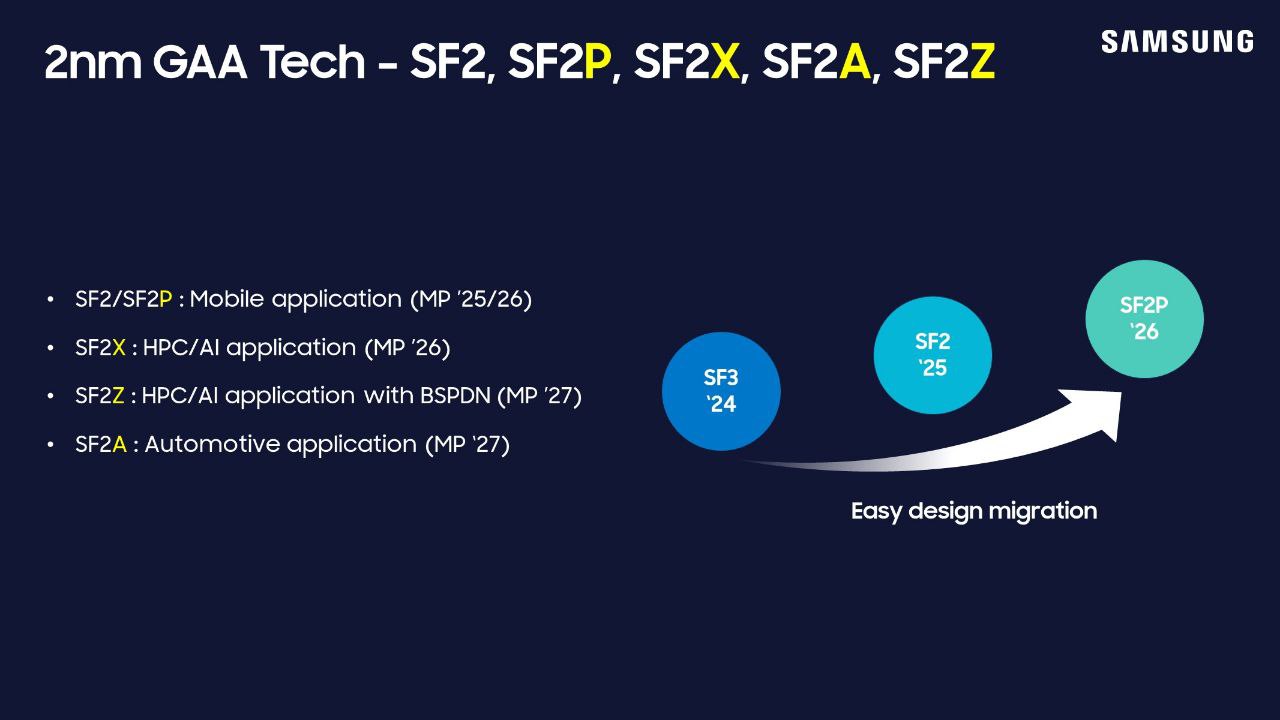
Meanwhile, this week's announcement also includes new information on Samsung's next batch of process nodes, which are planned for 2026 and 2027. In 2026 Samsung will have SF2P, a further refinement of SF2 which incorporates 'faster' yet less dense transistors. That will be followed up in 2027 with SF2Z, which adds backside power delivery to the mix for better and higher quality power delivery. In particular, Samsung is targetting voltate drop (aka IR drop) here, which is an ongoing concern in chip design.
Finally, SF1.4, a 1.4nm-class node, is on track for 2027 as well. Interestingly, however, it looks like it does not feature a backside power delivery. Which, per current roadmaps, would have Samsung as the only foundry not using BSPDN for their first 1.4nm/14Å-class node.
"We have optimized BSPDN and incorporated it for the first time in the SF2Z node we announced today," the spokesperso... Semiconductors

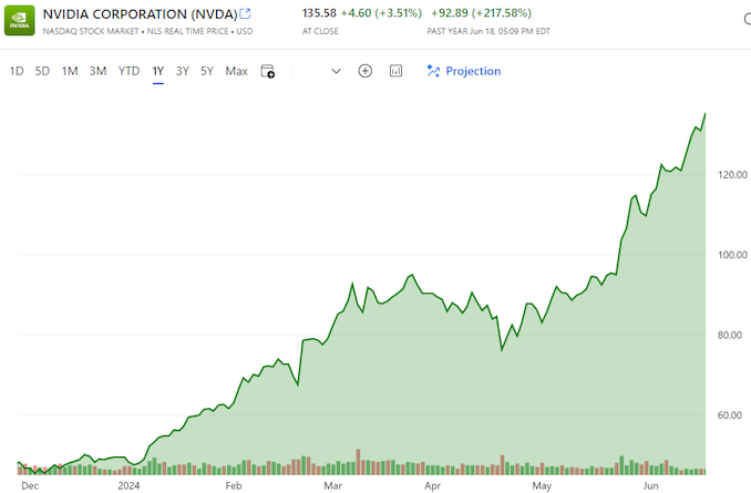
Thanks to the success of the burgeoning market for AI accelerators, NVIDIA has been on a tear this year. And the only place that’s even more apparent than the company’s rapidly growing revenues is in the company’s stock price and market capitalization. After breaking into the top 5 most valuable companies only earlier this year, NVIDIA has reached the apex of Wall Street, closing out today as the world’s most valuable company.
With a closing price of $135.58 on a day that saw NVIDIA’s stock pop up another 3.5%, NVIDIA has topped both Microsoft and Apple in valuation, reaching a market capitalization of $3.335 trillion. This follows a rapid rise in the company’s stock price, which has increased by 47% in the last month alone – particularly on the back of NVIDIA’s most recent estimates-beating earnings report – as well as a recent 10-for-1 stock split. And looking at the company’s performance over a longer time period, NVIDIA’s stock jumped a staggering 218% over the last year, or a mere 3,474% over the last 5 years.
NVIDIA’s ascension continues a trend over the last several years of tech companies all holding the top spots in the market capitalization rankings. Though this is the first time in quite a while that the traditional tech leaders of Apple and Microsoft have been pushed aside.
| Market Capitalization Rankings | ||
| Market Cap | Stock Price | |
| NVIDIA | $3.335T | $135.58 |
| Microsoft | $3.317T | $446.34 |
| Apple | $3.285T | $214.29 |
| Alphabet | $2.170T | $176.45 |
| Amazon | $1.902T | $182.81 |
Driving the rapid growth of NVIDIA and its market capitalization has been demand for AI accelerators from NVIDIA, particularly the company’s server-grade H100, H200, and GH200 accelerators for AI training. As the demand for these products has spiked, NVIDIA has been scaling up accordingly, repeatedly beating market expectations for how many of the accelerators they can ship – and what price they can charge. And despite all that growth, orders for NVIDIA’s high-end accelerators are still backlogged, underscoring how NVIDIA still isn’t meeting the full demands of hyperscalers and other enterprises.
Consequently, NVIDIA’s stock price and market capitalization have been on a tear on the basis of these future expectations. With a price-to-earnings (P/E) ratio of 76.7 – more than twice that of Microsoft or Apple – NVIDIA is priced more like a start-up than a 30-year-old tech company. But then it goes without saying that most 30-year-old tech companies aren’t tripling their revenue in a single year, placing NVIDIA in a rather unique situation at this time.
Like the stock market itself, market capitalizations are highly volatile. And historically speaking, it’s far from guaranteed that NVIDIA will be able to hold the top spot for long, never mind day-to-day fluctuations. NVIDIA, Apple, and Microsoft’s valuations are all within $50 billion (1.%) of each other, so for the moment at least, it’s still a tight race between all three companies. But no matter what happens from here, NVIDIA gets the exceptionally rare claim of having been the most valuable company in the world at some point.
(Carousel image courtesy MSN Money)
GPUs
Lorem Ipsum is simply dummy text of the printing and typesetting industry. Lorem Ipsum has been the industry's.


. According to the manufacturer, these key components are tailored to work efficiently together to deliver superior quiet cooling performance, rivalling many all-in-one water cooling systems and pushing the boundaries of air cooling efficiency.<a href="https://www.anandtech.com/show/21462/noctua-launches-new-flagship-cooler-nhd15-g2-with-lga1851-cpus-support"><img alt="" src="https://images.anandtech.com/doci/21462/nh_d15_g2_1_1_1_575px.jpg" /></a></p>
<p>Noctua offers the NH-D15 G2 in three versions to address the specific requirements of modern CPUs. The regular version is versatile and can be used for AMD's AM5 processors and Intel's LGA1700 CPUs with included mounting accessories. The HBC (High Base Convexity) variant is tailored for LGA1700 processors, especially those subjected to full ILM pressure or those that have deformed over time, ensuring excellent contact quality despite the concave shape of the CPU. Finally, the LBC (Low Base Convexity) version is tailored for flat rectangular CPUs, providing optimal contact on AMD's AM5 and other similar processors.</p>
<p style="text-align: center;"><a href="https://www.anandtech.com/show/21462/noctua-launches-new-flagship-cooler-nhd15-g2-with-lga1851-cpus-support"><img alt="" src="https://images.anandtech.com/doci/21462/specs_575px.png" /></a></p>
<p>While there are three versions of NH-D15 G2 aimed at different processors, they are all said to be compatible with a wide range of motherboards and other hardware. The new coolers' offset construction ensures clearance for the top PCIe x16 slot on most current motherboards. Additionally, they feature the upgraded Torx-based SecuFirm2+ multi-socket mounting system and come with Noctua's NT-H2 thermal compound.</p>
<p><a href="https://www.anandtech.com/show/21462/noctua-launches-new-flagship-cooler-nhd15-g2-with-lga1851-cpus-support"><img alt="" src="https://images.anandtech.com/doci/21462/nh_d15_g2_4_1_575px.jpg" /></a></p>
<p>For those looking to upgrade existing coolers like the NH-D15, NH-D15S, or NH-U14S series, Noctua is also releasing the NF-A14x25r G2 fans separately. These round-frame fans are fine-tuned in single and dual fan packages to minimize noise levels while offering decent cooling performance.</p>
<p>Finally, Noctua is also prepping a square-frame version of the NF-A14x25 G2 fan for release in September. This variant targets water-cooling radiators and case-cooling applications and promises to extend the versatility of Noctua's cooling solutions further.</p>
<p>All versions of Noctua's NH-D15 G2 coolers cost $149.90/€149.90. One NF-A14x25 G2 fan costs $39.90/€39.90, whereas a package of two fans costs $79.80/€79.80. The cooler is backed with a six-year warranty.</p>
</p> Cases/Cooling/PSUs)
. According to the manufacturer, these key components are tailored to work efficiently together to deliver superior quiet cooling performance, rivalling many all-in-one water cooling systems and pushing the boundaries of air cooling efficiency.<a href="https://www.anandtech.com/show/21462/noctua-launches-new-flagship-cooler-nhd15-g2-with-lga1851-cpus-support"><img alt="" src="https://images.anandtech.com/doci/21462/nh_d15_g2_1_1_1_575px.jpg" /></a></p>
<p>Noctua offers the NH-D15 G2 in three versions to address the specific requirements of modern CPUs. The regular version is versatile and can be used for AMD's AM5 processors and Intel's LGA1700 CPUs with included mounting accessories. The HBC (High Base Convexity) variant is tailored for LGA1700 processors, especially those subjected to full ILM pressure or those that have deformed over time, ensuring excellent contact quality despite the concave shape of the CPU. Finally, the LBC (Low Base Convexity) version is tailored for flat rectangular CPUs, providing optimal contact on AMD's AM5 and other similar processors.</p>
<p style="text-align: center;"><a href="https://www.anandtech.com/show/21462/noctua-launches-new-flagship-cooler-nhd15-g2-with-lga1851-cpus-support"><img alt="" src="https://images.anandtech.com/doci/21462/specs_575px.png" /></a></p>
<p>While there are three versions of NH-D15 G2 aimed at different processors, they are all said to be compatible with a wide range of motherboards and other hardware. The new coolers' offset construction ensures clearance for the top PCIe x16 slot on most current motherboards. Additionally, they feature the upgraded Torx-based SecuFirm2+ multi-socket mounting system and come with Noctua's NT-H2 thermal compound.</p>
<p><a href="https://www.anandtech.com/show/21462/noctua-launches-new-flagship-cooler-nhd15-g2-with-lga1851-cpus-support"><img alt="" src="https://images.anandtech.com/doci/21462/nh_d15_g2_4_1_575px.jpg" /></a></p>
<p>For those looking to upgrade existing coolers like the NH-D15, NH-D15S, or NH-U14S series, Noctua is also releasing the NF-A14x25r G2 fans separately. These round-frame fans are fine-tuned in single and dual fan packages to minimize noise levels while offering decent cooling performance.</p>
<p>Finally, Noctua is also prepping a square-frame version of the NF-A14x25 G2 fan for release in September. This variant targets water-cooling radiators and case-cooling applications and promises to extend the versatility of Noctua's cooling solutions further.</p>
<p>All versions of Noctua's NH-D15 G2 coolers cost $149.90/€149.90. One NF-A14x25 G2 fan costs $39.90/€39.90, whereas a package of two fans costs $79.80/€79.80. The cooler is backed with a six-year warranty.</p>
</p> Cases/Cooling/PSUs)
. According to the manufacturer, these key components are tailored to work efficiently together to deliver superior quiet cooling performance, rivalling many all-in-one water cooling systems and pushing the boundaries of air cooling efficiency.<a href="https://www.anandtech.com/show/21462/noctua-launches-new-flagship-cooler-nhd15-g2-with-lga1851-cpus-support"><img alt="" src="https://images.anandtech.com/doci/21462/nh_d15_g2_1_1_1_575px.jpg" /></a></p>
<p>Noctua offers the NH-D15 G2 in three versions to address the specific requirements of modern CPUs. The regular version is versatile and can be used for AMD's AM5 processors and Intel's LGA1700 CPUs with included mounting accessories. The HBC (High Base Convexity) variant is tailored for LGA1700 processors, especially those subjected to full ILM pressure or those that have deformed over time, ensuring excellent contact quality despite the concave shape of the CPU. Finally, the LBC (Low Base Convexity) version is tailored for flat rectangular CPUs, providing optimal contact on AMD's AM5 and other similar processors.</p>
<p style="text-align: center;"><a href="https://www.anandtech.com/show/21462/noctua-launches-new-flagship-cooler-nhd15-g2-with-lga1851-cpus-support"><img alt="" src="https://images.anandtech.com/doci/21462/specs_575px.png" /></a></p>
<p>While there are three versions of NH-D15 G2 aimed at different processors, they are all said to be compatible with a wide range of motherboards and other hardware. The new coolers' offset construction ensures clearance for the top PCIe x16 slot on most current motherboards. Additionally, they feature the upgraded Torx-based SecuFirm2+ multi-socket mounting system and come with Noctua's NT-H2 thermal compound.</p>
<p><a href="https://www.anandtech.com/show/21462/noctua-launches-new-flagship-cooler-nhd15-g2-with-lga1851-cpus-support"><img alt="" src="https://images.anandtech.com/doci/21462/nh_d15_g2_4_1_575px.jpg" /></a></p>
<p>For those looking to upgrade existing coolers like the NH-D15, NH-D15S, or NH-U14S series, Noctua is also releasing the NF-A14x25r G2 fans separately. These round-frame fans are fine-tuned in single and dual fan packages to minimize noise levels while offering decent cooling performance.</p>
<p>Finally, Noctua is also prepping a square-frame version of the NF-A14x25 G2 fan for release in September. This variant targets water-cooling radiators and case-cooling applications and promises to extend the versatility of Noctua's cooling solutions further.</p>
<p>All versions of Noctua's NH-D15 G2 coolers cost $149.90/€149.90. One NF-A14x25 G2 fan costs $39.90/€39.90, whereas a package of two fans costs $79.80/€79.80. The cooler is backed with a six-year warranty.</p>
</p> Cases/Cooling/PSUs | https://compbuddey.blogspot.com/2024/07/noctua-launches-new-flagship-cooler-nh_28.html)
. According to the manufacturer, these key components are tailored to work efficiently together to deliver superior quiet cooling performance, rivalling many all-in-one water cooling systems and pushing the boundaries of air cooling efficiency.<a href="https://www.anandtech.com/show/21462/noctua-launches-new-flagship-cooler-nhd15-g2-with-lga1851-cpus-support"><img alt="" src="https://images.anandtech.com/doci/21462/nh_d15_g2_1_1_1_575px.jpg" /></a></p>
<p>Noctua offers the NH-D15 G2 in three versions to address the specific requirements of modern CPUs. The regular version is versatile and can be used for AMD's AM5 processors and Intel's LGA1700 CPUs with included mounting accessories. The HBC (High Base Convexity) variant is tailored for LGA1700 processors, especially those subjected to full ILM pressure or those that have deformed over time, ensuring excellent contact quality despite the concave shape of the CPU. Finally, the LBC (Low Base Convexity) version is tailored for flat rectangular CPUs, providing optimal contact on AMD's AM5 and other similar processors.</p>
<p style="text-align: center;"><a href="https://www.anandtech.com/show/21462/noctua-launches-new-flagship-cooler-nhd15-g2-with-lga1851-cpus-support"><img alt="" src="https://images.anandtech.com/doci/21462/specs_575px.png" /></a></p>
<p>While there are three versions of NH-D15 G2 aimed at different processors, they are all said to be compatible with a wide range of motherboards and other hardware. The new coolers' offset construction ensures clearance for the top PCIe x16 slot on most current motherboards. Additionally, they feature the upgraded Torx-based SecuFirm2+ multi-socket mounting system and come with Noctua's NT-H2 thermal compound.</p>
<p><a href="https://www.anandtech.com/show/21462/noctua-launches-new-flagship-cooler-nhd15-g2-with-lga1851-cpus-support"><img alt="" src="https://images.anandtech.com/doci/21462/nh_d15_g2_4_1_575px.jpg" /></a></p>
<p>For those looking to upgrade existing coolers like the NH-D15, NH-D15S, or NH-U14S series, Noctua is also releasing the NF-A14x25r G2 fans separately. These round-frame fans are fine-tuned in single and dual fan packages to minimize noise levels while offering decent cooling performance.</p>
<p>Finally, Noctua is also prepping a square-frame version of the NF-A14x25 G2 fan for release in September. This variant targets water-cooling radiators and case-cooling applications and promises to extend the versatility of Noctua's cooling solutions further.</p>
<p>All versions of Noctua's NH-D15 G2 coolers cost $149.90/€149.90. One NF-A14x25 G2 fan costs $39.90/€39.90, whereas a package of two fans costs $79.80/€79.80. The cooler is backed with a six-year warranty.</p>
</p> Cases/Cooling/PSUs&body=https://compbuddey.blogspot.com/2024/07/noctua-launches-new-flagship-cooler-nh_28.html)


0 Comments